GOWIN GW1NR Series User manual

Gowin Programmer
User Guide
SUG502-1.1E,08/06/2018

Copyright©2018 Guangdong Gowin Semiconductor Corporation. All Rights Reserved.
No part of this document may be reproduced or transmitted in any form or by any denotes,
electronic, mechanical, photocopying, recording or otherwise, without the prior written
consent of GOWINSEMI.
Disclaimer
GOWINSEMI®, LittleBee®, Arora™, and the GOWINSEMI logos are trademarks of
GOWINSEMI and are registered in China, the U.S. Patent and Trademark Office, and other
countries. All other words and logos identified as trademarks or service marks are the
property of their respective holders, as described at www.gowinsemi.com. GOWINSEMI
assumes no liability and provides no warranty (either expressed or implied) and
is not responsible for any damage incurred to your hardware, software, data, or property
resulting from usage of the materials or intellectual property except as outlined in the
GOWINSEMI Terms and Conditions of Sale. All information in this document should be
treated as preliminary. GOWINSEMI may make changes to this document at any time
without prior notice. Anyone relying on this documentation should contact GOWINSEMI for
the current documentation and errata.

Revision History
Date
Version
Description
04/06/2017
1.0E
Initial version published.
08/06/2018
1.1E
Contents of device programming operation modified.

Contents
SUG502-1.1E
i
Contents
Contents...............................................................................................................i
List of Figures....................................................................................................iii
List of Tables......................................................................................................iv
1 About This Guide.............................................................................................1
1.1 Purpose .............................................................................................................................. 1
1.2 Supported Products............................................................................................................1
1.3 Related Documents............................................................................................................1
1.4 Abbreviations and Terminology...........................................................................................2
1.5 Support and Feedback .......................................................................................................2
2 Introduction......................................................................................................3
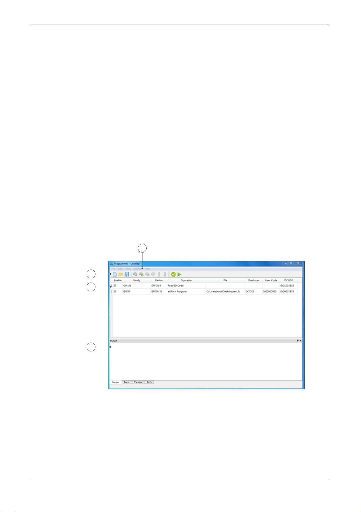
2.1 Device Table ....................................................................................................................... 3
2.2 Output Panel.......................................................................................................................4
3 Programming Download .................................................................................5
3.1 Download Cable Setting..................................................................................................... 5
3.2 Create New Project.............................................................................................................6
3.3 Open Existing Project.........................................................................................................6
3.4 Scan Daisy Chain...............................................................................................................7
3.5 Daisy Chain Configuration..................................................................................................7
3.5.1 Add Device....................................................................................................................... 7
3.5.2 Remove Device ...............................................................................................................9
3.5.3 Modify Device Position in Chain......................................................................................9
3.6 Device Programming Configuration.................................................................................... 9
3.6.1 SRAM Configuration...................................................................................................... 11
3.6.2 EmbFlash Configuration - GW1N (R) Series of FPGA Products................................... 11
3.6.3 ExFlash Configuration ................................................................................................... 11
3.7 Edit Pin State....................................................................................................................12
3.8 Key Programming.............................................................................................................13
3.9 Check the Current Configuration...................................................................................... 13
3.10 Save the Current Configuration to the Project File.........................................................14
3.11 Download Program .........................................................................................................14

List of Figures
SUG502-1.1E
iii
List of Figures
Figure 2-1 Gowin Programmer ..........................................................................................................3
Figure 3-1 Operation Process of Programming Download................................................................5
Figure 3-2 Cable Setting....................................................................................................................6
Figure 3-3 Device Table.....................................................................................................................7
Figure 3-4 Device Configuration........................................................................................................ 9
Figure 3-5 I/O State Editor.................................................................................................................12
Figure 3-6 Security Configuration...................................................................................................... 13
Figure 3-7 File Convertor...................................................................................................................14

List of Tables
SUG502-1.1E
iv
List of Tables
Table 2-1 Device Table....................................................................................................................... 4
Table 3-1 Cable Setting Parameters..................................................................................................6
Table 3-2 Device Configuration Parameters...................................................................................... 10
Table 3-3 Device Programming Configuration................................................................................... 10
Table 3-4 Security Configuration Parameters.................................................................................... 13

1About This Guide
1.1Purpose
SUG502-1.1E
1(14)
1About This Guide
1.1 Purpose
This guide describes how to use the Gowin Programmer. The software
screenshots and the supported products listed in this guide are based on
Windows 1.8.0 Beta. As the software is subject to change without notice,
some information may not remain relevant and may need to be adjusted
according to the software that is in use.
1.2 Supported Products
The information presented in this guide applies to the following
products:
GW1N(R) series of FPGA products: GW1N-1,GW1N-2,and
GW1N(R)-4.
GW2A(R) series of FPGA products: GW2A(R)-18 and GW2A-55.
1.3 Related Documents
The latest user guides are available on the Gowin website. Refer to
the related documents at www.gowinsemi.com:
Gowin Software User Guide
Gowin FPGA Product JTAG Configuration Manual
Gowin FPGA Product Configuration Manual

1About This Guide
1.4Abbreviations and Terminology
SUG502-1.1E
2(14)
1.4 Abbreviations and Terminology
Table 1-1 shows the abbreviations and terminology used in this guide.
Table 1-1 Abbreviations and Terminology
Abbreviations and Terminology
Full Name/Meaning
FPGA
Field Programmable GateArray
SRAM
Static Random Access Memory
I/O
Input/Output
BSDL
Boundary Scan Description Language
1.5 Support and Feedback
Gowin Semiconductor provides customers with comprehensive
technical support. If you have any questions, comments, or suggestions,
please feel free to contact us directly using the information provided below.
Website: www.gowinsemi.com
E-mail: [email protected]
Tel: +86 755 8262 0391

2Introduction
2.1Device Table
SUG502-1.1E
3(14)
2Introduction
The Gowin Programmer software generates the data stream file for
the FPGA. Before using, install the downloader first (it is installed by default)
and ensure that the download cable for the Gowin FPGA is connected, see
downloader in " Install > driver".
The Gowin Programmer view includes menu○
1, tool○
2, device table○
3,
and output panel○
4, as shown in Figure 2-1.
Figure 2-1 Gowin Programmer
1
2
3
4
①Menu
②Tool
③Device Table
④Output Panel
2.1 Device Table
In the device table, all the devices that will be programmed in daisy
chain are displayed via automatically scanning or manual configuration.
Each row in the table represents a device, and each column can be

2Introduction
2.2Output Panel
SUG502-1.1E
4(14)
displayed or hidden via the view options. The column options available in
the table are outlined in Table 2-1.
Table 2-1 Device Table
Options
Description
Enable
Editable, click to choose whether to program the device.
Note!
If "Enable" is not checked, the editor will be regarded as not
in the chain, and the row will be grayed out. Before editing
pins, security, programming download, etc., the device must
be removed from the daisy chain.
Vendor
Hidden by default.
Family
Editable, click to edit.
Device
Editable, click to edit.
Package
Hidden by default, editable, click to edit.
Operation
Non-editable, double-click to open the Device Configuration
Dialog to configure. Refer to 3.6 Device Programming
Configuration for the details.
File
Editable, click to edit.
Checksum
Non-editable, double-click to open the Device Configuration
Dialog to configure. Refer to 3.6 Device Programming
Configuration for the details.
User Code
Non-editable, double-click to open the Device Configuration
Dialog to configure. Refer to 3.6 Device Programming
Configuration for the details.
IR Length
Hidden by default.
IDCODE
Non-editable, double-click to open the Device Configuration
Dialog to configure. Refer to 3.6 Device Programming
Configuration for the details.
2.2 Output Panel
The output panel contains Output, Error, Warning, and Info, which
respectively display all the information related to error messages, warning
messages, etc.

3Programming Download
3.1Download Cable Setting
SUG502-1.1E
5(14)
3Programming Download
Programming download is the process of transferring data stream files
to the SRAM, embedded flash or external flash of FPGA via a download
cable. The programming download process is shown in Figure 3-1.
Figure 3-1 Operation Process of Programming Download
Start
Set
download line
Create or open a
project
Configure Daisy chain
and program
Download program
End
Check
configuration
rationality
Select the appropriate type, port, frequency etc. for
downloading programming.
Create a file for saving programming configuration or open
an existing project file for reading programming
configuration.
Configure Daisy chain in device table conforming to
physical connection status of Daisy chain, and select
program and the required data files for each device.
Download program for the configured Daisy chain. The final
result is shown in output panel.
Yes
No
3.1 Download Cable Setting
The Download Cable Setting functionality allows users to select the
available download cable type, port, and frequency for the programming
download. Gowin Programmer selects the first available download cable
port by default, with a frequency of 15M Hz by default.
Select "Edit > Setting > Cable" from the menu and open "Cable
Setting", as shown in Figure 3-2.

3Programming Download
3.2Create New Project
SUG502-1.1E
6(14)
Figure 3-2 Cable Setting
A description of the parameters that are available in the cable setting is
presented in Table 3-1.
Table 3-1 Cable Setting Parameters
Options
Description
Auto Detect
Automatically detects all download cables
connected to the computer. The first available
download cable will be selected by default.
Cable
Download cable type. GW - USB (FTDI) is selected
by default.
Port
Port available for download cable. The first
available port will be selected by default.
Frequency
Download cable frequency. Optional 30 MHz, 15
MHz, 2.5 MHz, 2 MHz, 1.5 MHz, 0.75 MHz, 0.1
MHz. The default is 2 MHz.
3.2 Create New Project
Note!
The current project will be closed if a new project is created.
Creating a new project results in the creation of a new file for saving
the programming configuration. Users can create new projects in three
ways:
A new project will be created automatically when the programmer is
opened.
In menu, select "File > New" to create a new project.
Click " " to create a new project.
3.3 Open Existing Project

3Programming Download
3.4Scan Daisy Chain
SUG502-1.1E
7(14)
Note!
The current project will be closed if a new project is opened.
Before opening the project file, set the download cable and ensure that the download
cable and daisy chain configuration are consistent in the project file. See 3.1
Download Cable Setting for details on setting the download cable. See 3.5 Daisy
Chain Configuration for details about the daisy chain configuration.
Opening an existing project involves opening the existing project file
and reading the programming configuration. Users can open an existing
project in two ways:
In menu, select "File > Open" to open an existing project.
Click " " to open an existing project.
3.4 Scan Daisy Chain
Programmer automatically scans the daisy chain connected to the
computer. The daisy chain can be scanned in two ways:
From the menu, select "Design > Scan.” The daisy chain connected to
the computer will be scanned.
Click on the " " icon to scan the daisy chain connected to the
computer.
After scanning, all devices are shown in the device table of the Gowin
Programmer in the order of chain, as shown in Figure 3-3.
Figure 3-3 Device Table
Note!
Some devices have the same ID (such as GW2A - 18 / GW2AR-18), which requires
users to manually specify the corresponding equipment after scanning.
3.5 Daisy Chain Configuration
Programmer supports the manual configuration of daisy chains. It
includes the ability to add a device, remove equipment, and modify the
position of the device in the chain.
3.5.1 Add Device
Follow the steps outlined below to add a device:
1. Select "Edit > Add Device" or click on the " " icon in the menu to add
a new device.

3Programming Download
3.5Daisy Chain Configuration
SUG502-1.1E
8(14)
2. Click "Family" to select the device using the drop-down menu.
3. Click "Device" to select a specific device type using the drop-down
menu.
Note!
When selected, the new device is added to the selected location or the end of the
daisy chain.

3Programming Download
3.6Device Programming Configuration
SUG502-1.1E
9(14)
3.5.2 Remove Device
Refer to following steps to remove a device:
1. Select the line containing the device.
2. Select "EditRemove Device" or click on the " " icon in the menu to
remove the device.
3.5.3 Modify Device Position in Chain
Refer to the following steps to modify the position of the device in the
chain:
1. Select the line containing the device.
2. Select "Edit > Up/Down" from the menu, or click on the " " or" "
icons to adjust the device position in the chain.
3.6 Device Programming Configuration
Select the line containing the device and open "Device Configuration"
using one of the following three ways:
1. Select "Edit > Configure Device" from the menu.
2. Click on the " " icon.
3. Double-click on the "Operation" option and open "Device
Configuration", as shown in Figure 3-4.
Figure 3-4 Device Configuration
The parameters available in the device configuration window are
described in Table 3-2.

3Programming Download
3.6Device Programming Configuration
SUG502-1.1E
10(14)
Table 3-2 Device Configuration Parameters
Name
Description
Access Mode
Select the programming mode of the device.
Operation
See Table 3-3 for programming operation of the
device.
Instruction Register
Length
For JTAG-NOOP, select the length of the device
command register.
Programming File
Select the programming data file.
Device
In external flash mode, select external flash model.
Start Address
In external flash mode, select the start address of
SPI flash. The minimum address unit is 1 Sector
(4096 Bytes).
Table 3-3 Device Programming Configuration
Access Mode
Operation
Description
SRAM Mode
Bypass
Bypass
Read ID Code
Read ID Code
Read Status
Register
Read Status Register
Reprogram
Reprogram
SRAM Program
SRAM Program
SRAM program and
Verify2
SRAM Program and Verify
Embedded
Flash Mode1
embFlash Erase,
Program
exFlash Erase,Program
embFlash Erase,
Program, Verify
embFlash Erase, Program, Verify
embFlash Erase
Only
embFlash Erase Only
External Flash
Mode
exFlash Erase,
Program3
embFlash Erase, Program.
exFlash Erase,
Program and Verify
exFlash Erase,Program and
Verify.
exFlash Erase Only
exFlash Erase Only.
exFlash Erase,
Program
in bscan
exFlash Erase,Program in
bscan.
exFlash Erase,
Program and Verify
in bscan
exFlash Erase,Program and
Verify in bscan.
exFlash Erase Only
in bscan
exFlash Erase Only in bscan.

3Programming Download
3.6Device Programming Configuration
SUG502-1.1E
11(14)
Note!
The GW2A/GW2AR series of FPGAproducts do not support embedded flash mode.
Security bit cannot be used in the FS file for SRAM verification.
When performing a non-boundary scan, ensure that config-mode [2:0] = 011
3.6.1 SRAM Configuration
Follow the steps outlined below to configure the SRAM mode:
1. Select the line containing the device.
2. Open "Device Configuration" using one of the three ways described
below:
a). Select "Edit > Configure Device" from the menu.
b). Click on the " " icon.
c). Double-click on the "Operation" option and open "Device
Configuration", as shown in Figure 3-4.
3. Select "SRAM Mode" in "Access Mode".
4. Select operation in "Operation" as required.
Note!
For JTAG-NOP (JTAG - NOP only support Bypass), you need to manually specify
the length of the instruction register or instruct the programmer to read the length
of the instruction register of the BSDL file.
5. Click "OK" to finish configuring.
3.6.2 EmbFlash Configuration - GW1N (R) Series of FPGA Products
The GW1N (R) series of FPGA Products include EmbFlash; the
corresponding programming model is embedded flash mode.
1. Select the line containing the device.
2. Open "Device Configuration” using one of the following three ways:
a). Select "Edit > Configure Device" from the menu options.
b). Click on the " " icon.
c). Double-click on the "Operation" option and open "Device
Configuration", as shown in Figure 3-4.
3. Select "Embedded Flash Mode" in "Access Mode".
4. Select operation in "Operation" as required.
5. Click on the “” icon corresponding to the "Programming File" to
select the programming data stream file.
6. Click "OK" to finish configuring.
3.6.3 ExFlash Configuration
The Gowin programmer supports ExFlash programming. The external
flash configuration process is as follows:
1. Select the line containing the device.
2. Open "Device Configuration" using one of the three methods described
below:
a). Select "Edit > Configure Device" from the menu options.
b). Click on the " " icon.
c). Double-click on the "Operation" option and open "Device
Configuration", as shown in Figure 3-4.

3Programming Download
3.7Edit Pin State
SUG502-1.1E
12(14)
3. Select "External Flash Mode" in "Access Mode".
4. Select operation in "Operation" as required. If "exFlash Program" is
selected in "Operation", the corresponding programming data stream
file needs to be selected in the "Programming File".
5. Select the external flash in "Device".
6. Select the starting address of the external Flash in "Start Address", by
default 0x00;
7. Click "OK" to finish configuring.
3.7 Edit Pin State
Programmer edits the I/O pin value via the I/O State Editor, which can
be set before running the download program. Refer to the following steps
to edit the pin state:
1. Select the line containing the device.
2. Select "Edit > Edit I/O State" from the menu options or right-click on the
line corresponding to the device. Select "Edit I/O State", and open the
"I/O State Editor", as shown in Figure 3-5.
3. Select the BSDL file that correlates with the device model and
package.
4. Change the pin state by clicking on the cell location or set the same
state for all pins by right-clicking on the menu.
Figure 3-5 I/O State Editor

3Programming Download
3.8Key Programming
SUG502-1.1E
13(14)
3.8 Key Programming
When programming with encrypted bitstream files, you need to write
the key of the bitstream file to FPGA. Select the line containing the device,
select "Edit > Configure Security" from the menu or right-click to select
"Configure Security". The "Security Configuration" window will appear, as
shown in Figure 3-6.
The total length of the key is 128 bits, and the initial state is 0x0, which
is a non-volatile and one-time programming fuse. Each bit that is written as
1 can't be changed to 0.
If locked, the key cannot be programmed and read.
Figure 3-6 Security Configuration
The parameters that are available in the security configuration window
are described in Table 3-4.
Table 3-4 Security Configuration Parameters
Name
Description
Write
Write the specified key value to FPGA.
Read
Read and display the key value in FPGAin the case
of unlocking.
Lock
Lock key in FPGA. The key cannot be read or
written after locking.
Note!
Programmer will prompt "lock" if the key has been locked. "Security Configuration" will not
display.
3.9 Check the Current Configuration
Before saving the files and downloading the program, you need to
check the current configuration.
Select "Design > Check" from the menu options or click on the " "
icon to check the current configuration is reasonable.
Other manuals for GW1NR Series
2
This manual suits for next models
6
Table of contents
Other GOWIN Motherboard manuals

GOWIN
GOWIN GW1N Series User manual

GOWIN
GOWIN DK-GoAI-GW2AR18QN88P User manual

GOWIN
GOWIN DK START GW2AR18 V1.1 User manual

GOWIN
GOWIN DK-START-GW1NR9 User manual

GOWIN
GOWIN EVAL-pSRAM-GW1NR4 Setup guide

GOWIN
GOWIN GW1N-1 User manual

GOWIN
GOWIN DK-START-GW2A18 User manual

GOWIN
GOWIN RISCV User manual

GOWIN
GOWIN GW1N-LV9LQ144C6I5 V1.1 User manual

GOWIN
GOWIN DK START GW1NZ-LV1FN32C6I5 User manual