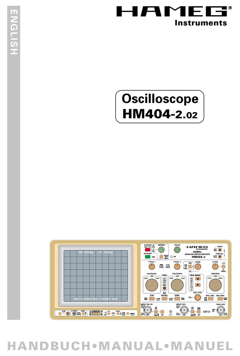
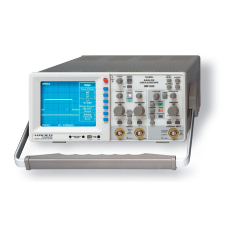
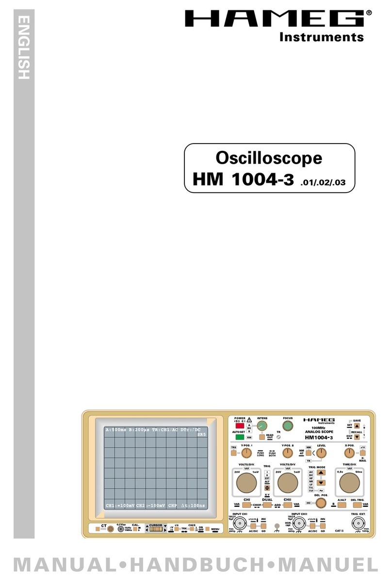
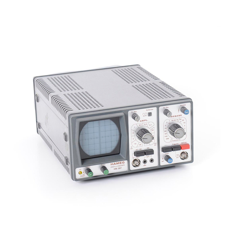
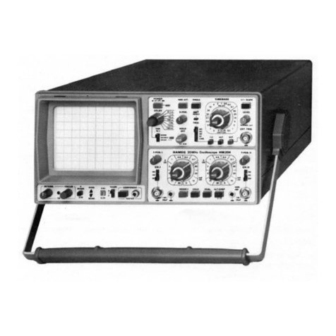
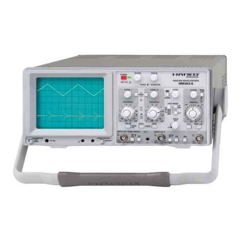
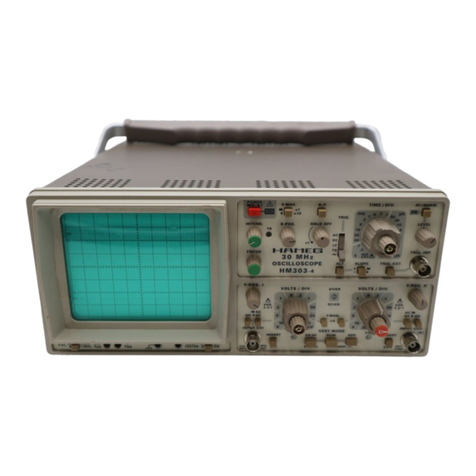
Hameg HM 203 User manual

MANUAL
Oscilloscope
HM 2 0 3
M E S S T E C H N IK

I — I W ^ l E i ■ 2 0 MHz OSCILLOSCOPE HM 203-4
S p ec ific atio n
Vertical Deflection (Y)
Bandwidth of both channels
DC to 20MHz (-3dB), DC to 28MHz (-6dB).
Risetime: «17.5ns. Overshoot: max. 1%.
Deflection coefficients: 1 2 calibr. steps,
5mV/cm to 20V/cm in 1-2-5 sequence,
with variable control uncal. 1:2.5 to 2mV/cm
Accuracy in calibrated position: ±3%.
Input impedance: 1 MQ II 28 pF.
Input coupling: DC-AC-GND.
Input voltage: max. 500V (DC + peak AC).
Operating modes
Channel I, Channel II, Channel I and II
alternate or chopped (chop freq. « 1 MHz),
sum or difference Ch. II ± Ch. I
(with Invert button for Channel I).
Timebase
Time coefficients: 18 calibrated steps,
0.5//s/cm to 0.2s/cm in 1 -2-5 sequence,
with variable control uncal. 1:2.5 to 0.2,us/cm,
with 5x magnification uncal. to 40ns/cm.
Accuracy in calibrated position: ±3%.
Trigger System
Modes: Auto or Normal (with level adj.).
Slope: positive or negative.
Sources: Ch. I, Ch. II, line, external.
Coupling: DC-AC-HF-LF (TV frame).
Threshold: internal 5mm, external 0.6V.
Bandwidth: DC up to 40MHz.
Horizontal Deflection (X)
Bandwidth: DC to 2.5MHz (-3dB).
Input: via Channel II (see Y deflection spec.).
X-Y phase shift: <3° up to 300kHz.
Component Tester
Test voltage: max. 8.5Vrms (open circuit).
Test current: max. 24mArms (shorted).
Test frequency: 50-60Hz (line frequency).
Test connection: 2 banana jacks 4mm dia.
One test lead is grounded (Safety Earth).
General Information
Cathode-ray tube: D14-362 P43/93 (med.),
P7/93 optional (long decay characteristic),
rectangular screen, internal graticule 8x1 Ocm.
Accelerating potential: 2000V.
Trace rotation: adjustable on front panel.
Calibrator: square-wave generator « 1 kHz
for probe compensation. Output 0.2V ±1 %.
Regulated DC power supplies: all operating
voltages including the high voltage.
Protective system: Safety Class I (IEC 348).
Line voltages: 110, 125, 220, 240V AC.
Permissible line fluctuation: ±10%.
Line frequency range: 50 to 60Hz.
Power consumption: 36 Watts (approx.).
Weight: 7kg (approx.). Color: techno-brown.
Cabinet (mm): W 285, H 145, D 380.
Subject to change.
Y: DC-20MHz, max. 2mV/cm X: 40ns/cm to 0.2s/cm
Triggering: DC to 4 0 MHz | | Component Tester
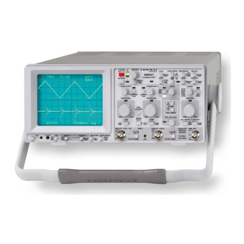
The already well-known good price/performance ratio of the
HM 2 0 3 -4 was again improved. Both vertical amplifiers now
have variable controls and an input sensitivity of max.
2m V/cm at full bandwidth. New is also that the sum and dif
ference of two signals can be displayed. The trigger facilities
were also extended. Besides Line- and TV-triggering, HF- and
DC-triggering are now possible, as well. At 5mm display
height the HM203 will trigger up to at least 40M H z. The
CRT's internal graticule permits parallax-free viewing from dif
ferent angles. Particularly for maintenance purposes, the
HM 203-4 also has a built-in Component Tester for quick tests
of semiconductors and other components, single or in-circuit.
The HM203 has been designed for general purpose applica
tions in industry and service. The multitude of operating
modes, concise layout of the front panels, and ease of opera
tion recommend it also for the training of engineers and
technicians
Accessories optional
Attenuator probes IX , 10X, 100X; demodulating probe;
various test cables; 50Q BIMC feed-through termination;
BNC-banana adapter; 4-Channel Amplifier; viewing hood.
Printed in West Germany (1 983) PI 2/83

Technical Details
General
The high performance and competitive price of the
HM203-4 has been achieved by the optimum use of
both discrete semiconductor and integrated circuit
technology. Quality and long term reliability are assured,
as only high quality components are selected for the
instrument. The well-arranged subassemblies combined
with a stable construction ensure easy servicing. The
subdivision of the complete circuitry into two large
printed circuit boards enables each component to be
easily reached, without dismantling any other parts.
A square-wave generator for probe compensation and a
trace rotation device are incorporated.
Each instrument is supplied with a comprehensive
manual including operating and servicing instructions,
circuit diagrams, and PCB layouts. It also contains test
instructions for checking the most important functions
by relatively simple means.
Modes of Operation
The HM203 can be used for single or dual trace opera
tion. Two time-related signals differing in waveform and
amplitude can be displayed either consecutively (alter
nate mode) or by the multiple switching of the channels
within one sweep period (chop mode). The sum or the
difference of two signals are displayed by algebraic addi
tion (Channel I can be inverted). When X-Y operation is
selected, the X input is via Channel II. Input impedance
and sensitivity ranges are then the same for both X and Y
deflection.
Vertical Deflection
The HM203 has two preamplifiers with diode-protected
FET inputs. These are electronically switched either
individually, alternately or together to the Y final
amplifier. The switching circuit operates with bistable-
controlled diode gates. Control for the alternate mode is
effected by the unblanking pulse from the sweep
generator and for the chopped mode by a 1 MHz signal.
The chop generator and the bistable multivibrator are
both combined in a single integrated circuit. The
preamplifier input stages utilize monolithic integrated
circuits to minimize drift. Exact measurement of the
displayed waveform is achieved by the 1 2-step frequen
cy compensated input attenuator calibrated in V/cm. In
order to obtain reliable triggering at higher frequencies,
the bandwidths of the preamplifiers are approximately
40MHz. The total bandwidth of the Y amplifier is
dependent on the output stage. The value stated refers to
-3dES (70% of 80mm).
Timebase and Triggering
The timebase of the HM 203 operates with a new type of
trigger technique developed by HAMEG. Here, the entire
trigger preparation is through a monolithic integrated
volage comparator whose TTL output is connected
directly to the control logic of the sweep generator. The
fast operation of this circuit means that very small signal
amplitudes up to a frequency of 4 0 MHz can be reliably
triggered. Using AC, DC, HF- or LF-filter coupling,
automatic or normal triggering from positive- or negative
going trigger edges can be selected from Channel I,
Channel II, Line or external sources. With the trigger
switch in the Auto position, a baseline is always
displayed even in the absence of a signal. The HM203
allows the triggering of TV signals (line or frame frequen
cy). A voltage-proof opto-coupler controls the unblank
ing of the CRT.
Component Tester
By simply pressing a single pushbutton, the HM203
can be switched into test mode without actually affect
ing the oscilloscope measuring set-up. The test result is
displayed on the screen in the way of a typical current-
voltage characteristic. Display height and width are con
stant. Test voltage and current are such that standard
semiconductors and other components cannot be
damaged. Components can be tested individually or
"in-circuit” . Easy and time-saving troubleshooting is
possible in complex circuitry by simple comparison with
an equivalent functioning circuit. Simply release the
Component Tester pushbutton to resume normal
oscilloscope measurements.
Examples of test displays
Short-circuit Z-diode below 8 volts Transistor base-collector Transistor base-emitter
paralleled to I^F + 68 00
P2 2/83

ACCESSORIES
HZ30 100MHz Oscilloscope Probe 10:1
Bandwidth DC-100MHz, Risetime 3.5ns. Maximum
input voltage 600V (DC + peak AC). Input impedance
10MQ. Input capacitance approx. 13pF, compensation
range 10-60pF. Cable length 1.5m. Supplied with
sprung hook, trimmer tool, spare tip, 1C tip, and
insulating tip.
HZ 35 Oscilloscope Probe 1:1
Bandwidth DC-10MF(z. Maximum input voltage 600V
(DC + peak AC). Input resistance equal to that of
oscilloscope. Input capacitance 47 pF + input
capacitance of oscilloscope. Cable length 1.5m. Sup
plied with sprung hook, insulating tip, 1C tip, and BNC
adapter.
HZ 36 Switchable Probe 1 0:1/1:1
This probe combines the specifications of the FIZ30 and
the FIZ35 in their respective attenuation ranges. In the
reference position the probe tip is grounded via a 9MQ
resistor, the oscilloscope input is connected directly to
ground. Cable length 1,5m. Supplied with sprung hook,
trimmer tool, spare tip, insulating tip, 1C tip, and BNC
adapter.
HZ37 High Voltage Probe 100:1
Bandwidth DC-50MFIz, Risetime 7ns. Maximum input
voltage 1500V (DC + peak AC). Input resistance
100MQ. Input capacitance approx. 4pF. Compensation
range 12-48pF. Cable length 1.5m. Supplied with
sprung hook, trimmer tool, insulating tip, 1C tip, and BNC
adapter.
HZ38 High Frequency Probe 10:1
Bandwidth DC-200MHz. Risetime 1.7ns. Maximum
input voltage 500V (DC + peak AC). Input resistance
10MQ. Input capacitance approx. 13pF. Compensation
range 12-48pF. Cable length 1.5m. Supplied with
sprung hook, trimmer tool, spare tip, 1C tip, insulating tip.
HZ39 Demodulator Probe
Bandwidth approx. 35kFlz-250MFIz RF input voltage
range 0.25Vrms to 40Vrms. Maximum input voltage
200V (DC + peak AC). Output polarity is positive. Cable
length 1.5m. Supplied with sprung hook, 1C tip,
insulating tip, and BNC adapter.
HZ32 Test Cable BNC-4mm
Coaxial test cable with BNC male plug at one end and
shielded banana-plug at the other. Cable length 1.15m.
Cable capacitance 126pF. Characteristic impedance
50Q. Maximum input voltage 500V (DC + peak AC).
HZ 34 Test Cable BIMC-BNC
Coaxial test cable with BNC male plugs at each end.
Cable length 1.2m. Cable capacitance 126pF.
Characteristic impedance 50£X Maximum input voltage
500V (DC + peak AC).
HZ 20 Adapter 4 mm to BNC
Two 4 mm binding posts 19 mm between centers to
standard BNC male plug. Maximum input voltage 500V
(DC + peak AC). Dimensions 42x35x1 8mm.
HZ22 5 0 Through-Termination
Should be used to terminate signal generators or coax-
cables with 5 0 0 characteristic impedance or when
measuring high frequency sine wave signals to avoid
standing waves. Maximum load 2W. Maximum voltage
lOVrms. Dimensions 14x20x62m m.
HZ42 Carrying Case
Suitable for Oscilloscopes FIM203-1, 203-3.
HZ43 Carrying Case
Suitable for Oscilloscopes HM31 2, 41 2, 51 2, 705.
HZ44 Carrying Case
Suitable for Oscilloscopes FIM307 and for FIZ62, 64.
HZ45 Carrying Case
Suitable for Oscilloscope FIM 103.
HZ46 Carrying Case
Suitable for Oscilloscope HM203-4, FIM204.
HZ47 Viewing Hood
Suitable for Oscilloscopes FIM203, 204, 705, 808.
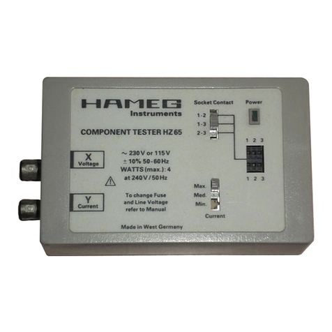
HZ 65 Component Tester
Works with any oscilloscope featuring X-Y operation. An
indispensable aid when repairing electronic equipment as
it displays the current-voltage characteristics of any com
ponent on the screen. Components can also be tested
"in-circuit” , with clear go / no go indication within
seconds. For low power transistors two sockets are pro
vided with switchable connections, facilitating tests of
each junction. Test currents of approx. 3.7mArms,
37mArms, and 320mArm s can be selected with slide
switch. Supplied with pair of test leads, two coax-cables
for scope, power cord. Safety Class II.
Printed in West Gemany (1 983)

OPERATING INSTRUCTIONS
General Information
The new HM203-4 is as easy to use as all HAMEG in
struments. Technologically it represents the latest state
of engineering in this price range. This is particularly
illustrated by the increased use of monolithic integrated
circuits. The logical arrangement of the controls and con
nectors on the front panel ensures that the user will
quickly become familiar with the operation of the instru
ment. However, even experienced operators are advised
to read the following instructions thoroughly, as they in
clude important information relating to the use of the
HM203-4.
The front panel is subdivided into three sections accord
ing to the various functions. The X-MAGN. X5 pushbut
ton, the calibrator output (CAL. 0.2V), and the COMPO
NENT TESTER pushbutton and its measuring socket are
located on the left directly below the screen of the
cathode-ray tube (CRT).
The X-Section, located on the upper right, contains the
red POWER pushbutton and indicating lamp, the IN-
TENS., FOCUS, and TR (trace rotation) controls. To the
right of them, all controls and switches for TIMEBASE
and triggering and the TRIG. EXT. input connector are
arranged.
The lower Y-Section contains the controls for the vertical
deflection system. On the right and left in this section are
located: vertical input connector, DC-AC-GD input cou
pling slide switch, Y-POS. control, AMPL. attenuator
switch with variable control, and ground jack. All these
controls and connectors exist in duplicate for each of the
Channels I and II. Four pushbuttons for selecting the
operating mode are arranged below the attenuator swit
ches: INVERT I, CHI/II — TRIG. I/II, DUAL, and
ALT/C H O P- I + 11
The instrument is so designed that even incorrect opera
tion will not cause serious damage. The pushbuttons
control only minor functions, and it is recommended that
before commencement of operation all pushbuttons are
in the " o u t" position. After this the pushbuttons can be
operated depending upon the mode of operation
required. For a better understanding of these Operating
Instructions the front panel picture at the end of these
instructions can be unfolded for reference alongside the
text.
The HM203 accepts all signals from DC (direct voltage)
up to a frequency of at least 20MHz (-3dB). For sine-
wave voltages the upper frequency limit will be
30-35 MHz. However, in this higher frequency range the
vertical display height on the screen is limited to approx.
4-5cm . In addition, problems of time resolution also
arise. For example, with 2 5 MHz and the fastest ad
justable sweep rate (40ns/cm), one cycle will be
displayed every 1 cm. The tolerance on indicated values
amounts to ±3% in both deflection directions. All values
to be measured can therefore be determined reatively ac
curately. However, from approximately 6 MHz upwards
the measuring error will increase as a result of loss of
gain. At 12MHz this reduction is about 10%. Thus, ap
proximately 11 % should be added to the measured
voltage at this frequency. As the bandwidth of the
amplifiers differ (normally between 20 and 2 5 MHz), the
measured values in the upper limit range cannot be
defined exactly. Additionally, as already mentioned, for
frequencies above 20MHz the dynamic range of the
display height steadily decreases. The vertical amplifier is
designed so that the transmission performance is not
affected by its own overshoot.
Warranty
Before being shipped each instrument must pass a 10
hour quality control test. Almost every early failure can be
detected by means of intermittent operation during this
test. Nevertheless, a component may fail but only after a
longer period of operation. Therefore, all HAMEG in
struments are under warranty for a period of one year,
provided that the instrument has not undergone any
modifications. HAMEG will repair or replace products
which prove to be defective during the warranty period.
No other warranty is expressed or implied. HAMEG is not
liable for consequential damages. It is recommended that
the instrument be repackaged in the original manner for
maximum protection. We regret that transportation
damage due to poor packaging is not covered by this
warranty.
In case of any complaint, attach a tag to the instrument
with a description of the fault observed. Please supply
name and department, address and telephone number to
ensure rapid service.
Safety
This instrument is designed and tested according to inter
national safety standards (e.g. IEC 348: Safety re
quirements for electronic measuring apparatus). The
instrument has left the factory in perfect safety condition.
To preserve this state and to ensure operation without
danger, the user must observe all advises and warning
remarks in these Operating, Test, and Service Instruc
tions. The case, chassis, and all measuring terminals
are connected to the Safety Earth conductor. The
specification of the instrument corresponds to Safety
Class / (three-conductor AC power cable). The grounded
accessible metal parts (case, sockets, jacks) and the
power line circuit of the HM203 are tested against one
Printed in West Germany (1 983) Ml 203-4
another with 1500V 50Hz. Under certain conditions,
5 0 Hz or 6 0 Hz hum voltages can occur in the measuring
circuit due to interconnection with other mains/line
powered instruments or devices. This can be avoided by
using a protective isolating transformer between the
mains/line outlet and power plug of the HM 203. Without
an isolating transformer, the instrument's power cable
must be plugged into an approved three-contact elec
trical outlet, which meets International Electrotechnical
Commission (IEC) safety standards.
Warning!
Any interruption of the protective conductor inside or
outside the instrument or disconnection of the protec
tive earth terminal is likely to make the instrument
dangerous. Intentional interruption is prohibited.
if a protective isolating transformer is used for the
display of signals with high zero potential, it should be
noted that these voltages are also connected to the
oscilloscope's case and other accessible metal parts.
Voltages up to 42 V are not dangerous. Higher
voltages, however, involve a shock hazard, in this
case, special safety measures must be taken and must
be supervised by qualified personnel.
As with most electron tubes, the cathode-ray tube
develops X-rays. With the HM203 the dose equivalent
rate falls far below the maximum permissible value of
36pA/kg.
Operating Conditions
Admissible ambient temperature range during operation:
+ 1 0°C ... + 40°C. Admissible ambient temperature
range for storage or transportation: — 40°C
... + 70°C. If condensed water exists in the instrument it
should not be turned on before acclimatization is
achieved. In some cases (an extremely cold oscilloscope)
about two hours should be allowed before putting the in
strument into operation. The instrument should be placed
in a clean and dry room In other words, the instrument
may not be put into operation in explosive, corrosive,
dusty, or moist environments. The instrument may be
operated in any position, however, the convection cool
ing must not be impaired. Therefore, when the instru
ment is in continuous operation it should be used in the
horizontal position preferably on its tilt stand.
The instrument must be disconnected and secured
against unintentional operation if there is any presump
tion that safe operation is not possible. This supposition
is qualified
— if the instrument has visible damage,
— if the instrument has loose parts,
— if the instrument does not function,
— after a long storage under unfavourable
circumstances (e.g. out of doors or in moist
environments),
— after excessive transportation stress (e.g. in poor
packaging).
Use of the Tilt Handle
The handle of the oscilloscope can be fixed in three posi
tions, one for use as a carrying handle and two positions
as a tilt stand. With the tilt handle the instrument can be
inclined 10° or 20° to the horizontal.
Handling is as follows:
— Place the HM203 on its rear feet. The front drop-in
pins in the hinges will fall back into the front groove of
the notched discs (fixed on cabinet).
— Pull the handle only about 5 mm out of its locking posi
tion and turn it towards the lower edge of the front
panel.
— Lock the handle into the required position by pushing it
back towards the hinges.
— Place the instrument in its work area.
First Time Operation
Check that the instrument is set to the correct
mains/line voltage.
On delivery, the instrument is set to AC 240V ±10%
(50-60Hz) mains/line voltage. The power plug-in unit at
the rear contains the three-pin power connector. For this
a three wire power cord with triple-contact connector
and three-pole power plug is required. The unit also con-
M2 203-4

tains the power fuse, which is interchangeable for the dif
ferent mains/line voltages. The fuse holder with its
square top plate can be pulled out, and changing of the
mains/line voltage is possible by turning this plate 90
degrees for each of the four voltages marked on the plate
(see triangle on the rear panel below the fuse holder).
The fuse holder should then be plugged in again in the
desired position, which should be the closest value of
the measured mains/line voltage in your area The set
value is always readable on the lower edge of the fuse
holder. The power fuse must correspond to the voltage
selected and when necessary should be replaced. The
type and rated current are given on the rear panel and in
the Service Instructions.
Before applying power to the oscilloscope, it is recom
mended that the following simple procedures are per
formed:
— Check that all pushbuttons are in the out position, i.e.
released.
— Rotate the three variable controls with arrows, i.e.
TIMEBASE variable control, CH.I and CH.II at
tenuator variable controls, fully counterclockwise in
their calibrated detent.
— Set the control knobs with marker lines to their mid
range position (marker lines pointing vertically).
— The slide switch in the X-Section should be set to its
uppermost AC position.
— Both input coupling slide switches for CH. I and CH. II
in the Y-Section should be set to the GD position.
Switch on the oscilloscope by depressing the red
POWER pushbutton. An LED will illuminate to indicate
the working order. The trace, displaying one baseline,
should be visible after a short warm-up period of 10
seconds. Adjust Y-POS.I and X-POS. controls to center
the baseline. Adjust INTENS, (intensity) and FOCUS
controls for medium brightness and optimum sharpness
of the trace. The oscilloscope is now ready for use.
If only a spot appears (CAUTION! CRT phosphor can be
damaged.), reduce the intensity immediately and check
that the HOR. EXT. pushbutton is in the released (out)
position. If the trace is not visible, check the correct posi
tions of all knobs, buttons, and switches (particularly
AT/NORM. button in out position).
To obtain the maximum life from the cathode-ray tube,
the minimum intensity setting necessary for the measure
ment in hand and the ambient light conditions should be
used Particular care is required when a single spot is
displayed, as a very high intensity setting may cause
damage to the fluorescent screen of the CRT. Switching
the oscilloscope off and on at short intervals stresses the
cathode of the CRT and should therefore be avoided.
In spite of Mumetal-shielding of the CRT, effects of the
earth's magnetic field on the horizontal trace position
cannot be completely avoided. This is dependent upon
the orientation o f the oscilloscope on the place of
work. A centred trace may not align exactly with the
horizontal center line of the graticule. A few degrees of
misalignment can be corrected by a potentiometer
accessible through an opening on the front panel
marked TR.
DC Balance Adjustment
The vertical preamplifiers for CH.I and CH.II contain in
put source followers with matched dual FETs. After long
periods of use the FET characteristics may change which
can alter the DC balance of the vertical amplifier.
A quick check can be made on each channel by rotating
the variable control knob on the attenuator switch to and
fro, clockwise and back to the calibrated detent C. If the
trace moves from the vertical position (up or down) by
more than 1 mm, the DC balance will require readjust
ment. This check should be made after a 20 minute
warm-up period.
Adjustment procedure
The following instructions should be performed to obtain
the correct DC balance adjustment of both channels.
— Remove all input cables and adjust oscilloscope con
trols to display the baseline.
— Center the baseline using Y-POS. and X-POS. con
trols.
— Set attenuator switches to 5mV/cm and input cou
pling switches to GD.
— Release all pushbuttons in the Y-Section.
— Place the oscilloscope so that it rests firmly on its back
(upright position) and locate DC balance adjustment
potentiometer access holes — marked CH.I DC-
BALANCE CH.II - which are found underneath the
instrument.
— Insert a screwdriver (blade approx. 3 mm, length min.
20mm) in CH.I hole. Behind the hole, a plastic funnel
with slotted bottom is located.
— Rotate AMPL. I variable control to and fro and adjust
balance pot so that the baseline no longer moves up or
down. When the trace remains steady, correction of
CH.I is completed.
— Depress CHI/II button. Repeat adjustment procedure
for CH.II
Probe Adjustment
To achieve the undistorted display of signals when using
an X I0 or X I 00 attenuator probe, the probe must be
M3 203-4

compensated to match the input impedance of the ver
tical amplifier. This can be easily achieved as the HM203
has a built-in square-wave generator with a repetition fre
quency of approx. 1 kHz and an output voltage of
0 .2 Vpp ± 1 %
The method employed is as follows. The probe tip with
its sprung hook is connected to the output eyelet
designated by CAL. (calibrator) on the front panel of the
instrument. The probe trimmer is then adjusted by using
the trimming tool supplied. The correct display is shown
in the following figure.
incorrect correct incorrect
The TIMEBASE switch should be in the 0.2ms/cm posi
tion. The input coupling is set to DC. If the attenuator
sensitivity is set to 5mV/cm (variable control to C), the
display will have a height of 4cm when an X I 0 probe is
being compensated. As an attenuator probe is constantly
subjected to considerable stresses, the compensation
should be frequently checked.
It should be noted that the frequency of the square-wave
generator is unsuitable for the time calibration. Further
more, the pulse duty factor has not the 1:1 value. Finally,
the rise and fall times of the square signal are so fast that
the edges — even with maximum intensity — are visible
only with difficulty. This is not a flaw, but actually the
precondition for a simple and exact probe compensation
(or a deflection coefficient check) like horizontal pulse
tops, calibrated pulse amplitude, and zero potential on
the negative pulse top.
Type of Signal
All types of signals whose frequency spectrum is below
20MHz can be displayed on the HM203. The display of
simple electrical processes such as sinusoidal RF and AF
signals or ripple voltage poses no problems. However,
when square or pulse-shaped signals are displayed, it
must be remembered that their harmonic content must
also be transmitted. In this case, the bandwidth on the
vertical amplifier must be considerably higher than the
repetition frequency of the signal. In view of this, ac
curate evaluation of such signals with the HM203 is only
possible up to a maximum repetition rate of 2 MHz.
Operating problems can sometimes occur when com
posite signals are to be displayed, especially if they do
not contain any suitable level components and repetition
frequency which can be used for triggering. This occurs,
for example, with burst signals. To obtain a stably trig
gered display in these cases, it may be necessary to use
Normal Triggering and/or the TIMEBASE variable con
trol. Television video signals are relatively easy to trig
ger. However, when investigating signals at frame rate,
the TRIGGER SELECTOR slide switch has to be set in LF
position (low-pass filter). In this mode, the more rapid
line pulses are attenuated so that, with appropriate level
adjustment, triggering can easily be carried out on the
leading or trailing edge of the frame synchronizing pulse.
For optional operation as a DC or AC voltage amplifier,
each channel is provided with a DC-AC coupling switch.
The DC position should only be used with an attenuator
probe or at very low frequencies or if the determination of
the DC voltage content of the signal is absolutely
necessary.
However, when investigating very low-frequency pulses,
disturbing ramp-offs may occur with AC coupling. In this
case, DC operation is to be preferred if the signal voltage
is not superimposed on a too high DC voltage level.
Otherwise, a capacitor of adequate capacitance must be
connected before the input of the vertical amplifier
(switched to DC coupling). It should be remembered that
this capacitor must have a sufficiently high breakdown
voltage. DC operation is also recommended for the
display of logic and pulse signals, particularly if their
pulse duty factor changes permanently during operation.
Otherwise, the display will move up and down with any
change. DC voltages can only be measured in the DC
position.
Amplitude Measurements
In general electrical engineering, alternating voltage data
normally refers to effective values (rms = root-mean-
square value). However, for signal magnitudes and
voltage designations in oscilloscope measurements, the
peak-to-peak voltage (Vpp) value is applied. The latter
corresponds to the real potential difference between the
most positive and most negative points of a signal
waveform.
If a sinusoidal waveform, displayed on the oscilloscope
screen, is to be converted into an effective (rms) value,
the resulting peak-to-peak value must be divided by
2x|/2 = 2.83. Conversely, it should be observed that
sinusoidal voltages indicated in Vrms (Veff) have 2.83
times the potential difference in Vpp. The relationship
between the different voltage magnitudes can be seen
from the following figure.
S»
rr
\
M4 203-4

Voltage values of a sine curve
Vrms = effective value; Vp = simple peak or crest value;
Vpp = peak-to-peak value; Vmom = momentary value.
The minimum signal voltage required at the vertical
amplifier input for a display of 1cm is approximately
2mVpp. This is achieved with the AMPL. attenuator
control set at 5mV/cm and its variable control in the ful
ly clockwise position. However, smaller signals than
this may also be displayed. The deflection coefficients
on the input attenuators are indicated in mV/cm or V/cm
(peak-to-peak value).
For exact amplitude measurements, the variable con
trol on the attenuator switch must be set to its
calibrated detent C.
The magnitude of the applied voltage is ascertained by
multiplying the selected deflection coefficient by the
vertical display height in cm.
If an attenuator probe X I 0 is used, a further
multiplication by a factor o f 10 is required to ascertain
the correct voltage value.
With direct connection to the vertical input, signals up to
160Vpp may be displayed.
With the designations
H = display height in cm,
U = signal voltage in Vpp at the vertical input,
D = deflection coefficient in V/cm at attenuator switch,
the required quantity can be calculated from the two
given quantities:
U = D H H = — D = —
D H
However, these three values are not freely selectable.
They have to be within the following limits (trigger
threshold, accuracy of reading):
H between 0.5 and 8cm, if possible 3.2 to 8cm,
U between 2.5mVpp and 160Vpp,
D between 5mV/cm and 20V/cm in 1 -2 -5 sequence.
Examples:
Set deflection coefficient D = 50mV/cm — 0.05V/cm,
observed display height H = 4.6cm,
required voltage U = 0.05 • 4.6 = 0.23Vpp.
Input voltage U = 5Vpp,
set deflection coefficient D = 1 V/cm,
required display height H = 5:1 = 5cm.
Signal voltage U = 220Vrms- 2 • j/2 = 622 Vpp
(voltage > 1 60Vpp, with probe X I 0: U = 62.2Vpp),
desired display height H = min. 3.2cm, max. 8cm,
max. deflection coefficient D= 62.2:3.2 = 1 9.4V/cm,
min. deflection coefficient D= 62.2:8 =7.8V/cm ,
adjusted deflection coefficient D = 10V/cm.
If the applied signal is superimposed on a DC (direct
voltage) level, the total value (DC + peak value o f the
alternating voltage) of the signal across the Y-input
must not exceed ±500V . This same limit applies to nor
mal attenuator probes X10, the attenuation ratio of
which allows signal voltages up to approximately
1,000Vpp to be evaluated. Voltages of up to approx
imately 3,000Vpp may be measured by using the HZ37
high voltage probe which has an attenuation ratio of
100:1 . It should be noted that its Vrms value is derated
at higher frequencies (see page M7: Connection of Test
Signal). If a normal X I0 probe is used to measure high
voltages, there is the risk that the compensation trimmer
bridging the attenuator series resistor will break down
causing damage to the input of the oscilloscope.
However, if for example only the residual ripple of a high
voltage is to be displayed on the oscilloscope, a normal
X I0 probe is sufficient. In this case, an appropriate high
voltage capacitor (approx. 22-68nF) must be connected
in series with the input tip of the probe.
It is very important that the oscilloscope input coupling is
set to DC, if an attenuator probe is used for voltages
higher than 500V (see page M7: Connection of Test
Signal).
With input coupling switched to GD and with the Y-POS.
control, a horizontal graticule line can be adjusted as a
reference axis for ground potential. It can be placed
underneath, on, or above the horizontal center line, as
the case may be to measure positive and/or negative
deviations from ground potential. Some switchable
probes have a built-in reference switch position for the
same application.
Time Measurements
As a rule, all signals to be displayed are periodically
repeating processes and can also be designated as
periods. The number of periods per second is the recur
rence frequency or repetition rate. One or more signal
M5 203-4

periods or even part of a period may be shown as a func
tion of the adjustment of the TIMEBASE switch. The time
coefficients on the TIMEBASE switch are indicated in
ms/cm and pslcm. Accordingly, the dial is subdivided
into two sectors.
The duration of a signal period or a portion of the
waveform is ascertained by multiplying the relevant
time (horizontal distance in cm) by the time coefficient
selected on the TIMEBASE switch.
The time variable control (small knob on the
TIMEBASE switch) must be in its calibrated detent (C)
for accurate measurement (arrow horizontal and poin
ting to the left).
With the designations
L = displayed wave length in cm of one period,
T = time in seconds for one period,
F = recurrence frequency-in Hz of the signal,
Tc = time coefficient in s/cm on timebase switch
and the relation F = 1/T, the following equations can be
stated:
T =
F =
L Tc
1
L Tc
L = Tc
L = F T c
Tc = r
Tc = L F
However, these four values are not freely selectable.
They have to be within the following limits:
L between 0.2 and 10cm, if possible 4 to 10cm,
T between 0.0bps and 2 s,
F between 0.5Hz and 20MHz,
Tc between 0.5/is/cm and 200ms/cm in 1-2-5 se
quence (with X-MAGN. X5 button in out position).
With depressed X-MAGN. X5 pushbutton the Tc value
must be divided by 5.
Examples:
Displayed wavelength L = 7cm,
set time coefficient Tc = 0.5^s/cm,
required period T = 7 0.5 • 10 6 = 3.5/is
required rec. freq. F = 1: (3.5 • 10 6) = 286kHz.
Signal period T = 0.5s,
set time coefficient Tc = 0.2s/cm,
required wavelength L = 0.5:0.2 = 2.5cm.
Displayed ripple wavelength L = 1 cm,
set time coefficient Tc = 10ms/cm,
required ripple freq. F = 1:(1 • 10• 1 0 3) = 100Hz.
TV-line frequency F = 1 5 625 Hz,
set time coefficent Tc = 10yus/cm,
required wavelength L = 1 : (1 5 625 • 10 5) = 6.4cm.
Sine wavelength L = min. 4cm, max. 10cm,
Frequency F = 1 kHz,
max. time coefficient Tc = 1 :(4 • 103) = 0.25ms/cm,
min. time coefficient Tc = 1: (10 • 103) = 0.1 ms/cm,
set time coefficient Tc = 0 .2ms/cm,
required wavelength L = 1 :(1 0 3 0 .2 -1 0 3) = 5cm.
Displayed wavelength L = 0.8cm,
set time coefficient Tc = 0.5yus/cm,
pressed X-MAGN. X5 button: Tc = 0.1 pslcm,
required rec. freq. F = 1:(0.8-0.1 • 1 0 6) = 12.5MHz,
required period T = 1 :(1 2.5 • 106) = 80ns.
If the time is relatively short as compared with the com
plete signal period, an expanded time scale should
always be applied (X-MAGN. X5 button depressed). In
this case, the ascertained time values have to be divided
by 5.
When investigating pulse or square waveforms, the
critical feature is the risetime of the voltage step. To
ensure that transients, ramp-offs, and bandwidth limits
do not unduly influence the measuring accuracy, the
risetime is generally measured between 10% and 30%
of the vertical pulse height. For peak-to-peak signal
amplitudes of 5cm height, which are symmetrically ad
justed to the horizontal center line, the internal graticule
of the CRT has two horizontal dotted lines + 2 .5cm from
the center line. Adjust'the Y attenuator switch with its
variable control together with the Y-POS. control so that
the pulse height is precisely aligned with these 0 and
100% lines. The 10% and 90% points of the signal will
now coincide with the two lines, which have a distance
of + 2cm from the horizontal center line and an additional
subdivision of 0.2 cm. The risetime is given by the pro
duct of the horizontal distance in cm between these
two coincidence points and the time coefficient set
ting If magnification is used, this product must be divid
ed by 5. The fall time of a pulse can also be measured by
using this method.
The following figure shows correct positioning of the
oscilloscope trace for accurate risetime measurement.
100%
90%
10%
0
M6 203-4
With a time coefficient of 0.5//s/cm and depressed
X-MAGN. X5 pushbutton, the example shown in the
above figure results in a measured total risetime of
ttot = 1,6cm -0.5jus/cm : 5 = 160ns
When very fast risetimes are being measured, the
risetime of the oscilloscope amplifier has to be deducted
from the measured time value. The risetime of the signal
can be calculated using the following formula.
tr = 1 / ttot2 — tosc2
In this ttot is the total measured risetime, and tosc is the
risetime of the oscilloscope amplifier (approx. 17.5ns
with HM203). If ttot is greater than 100ns, then ttot can
be taken as the risetime of the pulse, and calculation is
unnecessary (error smaller than 1 %).
Connection of Test Signal
The signal to be displayed should be fed to the vertical in
put of the oscilloscope by means of a shielded test cable,
e.g. the HZ32 or HZ34, or by a X I0 or X I00 attenuator
probe. The use of these shielded cables with high im
pedance circuits is only recommended for relatively low
frequencies (up to approx. 50kHz). For higher frequen
cies, and when the signal source is of low impedance, a
cable of matched characteristic impedance (usually
50Q) is recommended. In addition, and especially
when investigating square or pulse waveforms, a
resistor equivalent to the characteristic impedance of
the cable must also be connected to the cable directly
at the input of the oscilloscope. When using a 50Q
cable, such as the HZ34, a 50Q through-termination
type HZ22 is available from HAMEG. When investigating
square or pulse waveforms with fast risetimes, transient
phenomena on both the edge and top of the signal may
become visible if the correct termination is not used. It
must be remembered that the 50Q through-termination
will only dissipate a maximum of 2 watts. This power
consumption is reached with lOVrms or with 28Vpp
sine signal. If a X I 0 attenuator probe (e.g. HZ30) is
used, no termination is necessary. In this case, the con
necting cable is matched directly to the high impedance
input of the oscilloscope. When using attenuator probes,
even high internal impedance sources are only slightly
loaded (by approximately 10MQI112pF). Therefore,
when the voltage loss due to the attenuation of the probe
can be compensated by a higher sensitivity setting on the
HM203, the probe should always be used. Also it should
be remembered that the series impedance of the probe
provides a certain amount of protection for the input of
the oscilloscope amplifier. It should be noted that all
attenuator probes must be compensated in conjunction
with the oscilloscope (see: Probe Adjustment, page M4).
If a X I 0 or X I 00 attenuator probe is used, the DC
input coupling must always be set. With AC coupling,
the attenuation is frequency-dependent, the pulses
displayed can exhibit ramp-off, DC-voltage contents are
suppressed — but loads the respective input coupling
capacitor of the oscilloscope. The electric strength of
which is maximum 500V (DC-(-peak AC). For the sup
pression of unwanted DC voltages, a capacitor of ade
quate capacitance and electric strength may be con
nected before the input tip of the probe (e.g. for ripple
measurements).
With the HZ37 X I 00 probe, the permissible AC input
voltage is frequency-dependent limited:
below 20kHz (TV line frequency!) up to
max. 1.500Vp - 3.000Vpp - 1.061 Vrms;
above 20kHz (with f in MHz) up to
212 w ^ 424 „ A 150 „

max. Vp a —— Vpp - —=- Vrms.
F F F
It is important to remember that when low voltage signals
are being investigated the position of the ground point on
the test circuit can be critical. This ground point should
always be located as close as possible to the measuring
point. If this is not done, serious signal deformation may
result from any spurious currents through the ground
leads or test chassis parts. This comment also applies to
the ground leads on attenuator probes which ideally
should be as short and as thick as possible. For the con
nection of a probe to a BNC socket, a BNC-adapter
should be used. It forms often a part of the probe
accessory. Grounding and matching problems are then
eliminated.
The location and quantitative measurement of a
magnetic leakage (e.g. from power transformer) into a
circuit is possible using a pick-up coil. If the coil has many
windings, it should be shielded against static fields (non
magnetic shield without short-circuited turn). Also the in
terconnection between coil and oscilloscope vertical in
put should be made by a shielded cable with BNC male
connector at one end. A resistor of approx. 100Q should
be connected in series between cable core and connec
tor core. This resistor attenuates radio-frequency excita
tion. The shieldings prevent any undesired capacitive
couplings. During measurement, use line triggering
(TRIGGER SELECTOR switch to LINE)
Hum or interference voltage appearing in the measuring
circuit (especially with a small deflection coefficient) is
possibly caused by multiple grounding, because through
it equalizing currents can flow in the shieldings of the
measuring cables (voltage drop between the non-fused
M7 203-4

earthed conductors of other line powered devices, which
are connected to the oscilloscope or test object, e.g.
signal generators with anti-interference capacitors).
Sometimes the trace will disappear after an input signal
has been applied. The attenuator switch must then be
turned back to the left, until the vertical signal height is
only 3-8cm. With a signal amplitude greater than
1 60Vpp, an attenuator probe must be inserted before
the oscilloscope's vertical input. If, after applying the
signal, the trace is nearly blanked, the period of the signal
is probably substantially longer than the set value on the
TIMEBASE switch. It should be turned to the left on an
adequately greater time coefficient.
Caution: When connecting unknown signals to the
oscilloscope input, always use automatic triggering and
set the DC-AC input coupling switch to AC. The at
tenuator switch should initially be set to 20V/cm.
Operating Modes of the Y Amplifier
The required operating modes are selected on four
pushbuttons located in the Y-Section. For Mono opera
tion, all pushbuttons should be in the out position, the
instrument is then operating on Channel I only Vox Mono
operation with ChannelH, the CHI/II pushbutton has to
be pressed. Automatically, the internal trigger voltage is
derived from Channel II. When the DUAL button is
depressed, the HM203 is in Dual channel operation. In
this mode, the channels are displayed consecutively
(alternate mode). This mode is not suitable for the display
of very low frequency signals (< 1 kHz), as the trace will
appear to flicker or jump. Under these conditions, the
ALT/CHOP button should be depressed additionally
selecting chopped mode. In this position, both channels
then share the trace during each sweep period. For the
display of high frequency signals, the type of channel
switching selected is less important.
To select the Add mode, only the ALT/CHOP (I+ 11) but
ton should be depressed. The signals on both channels
are then added together. If in this mode Channel I is
inverted (pushbutton INVERT I depressed), then the dif
ference between the two channels is displayed. For both
of these operating modes, the vertical position of the
trace depends on the setting of the Y-POS. controls of
both channels.
For X -Y operation, the pushbutton in the X-Section
marked HOR. EXT. must be depressed. The X signal is
then derived from the Channel II (HOR. INP.). The
calibration of the X signal during X-Y operation is
determined by the setting of the Channel H input
attenuator and variable control. This means that the
sensitivity ranges and input impedances are identical for
both the X and Y axes. However, the Y-POS. II control is
disconnected in this mode. Its function is taken over by
the X-POS. control. It is important to note that the
X-MAGN. X5 pushbutton switch, normally used for
expanding the sweep, should not be operated in the X-Y
mode. It should also be noted that the bandwidth of the X
amplifier is approximately 2.5 MHz (-3dB), and therefore
an increase in phase difference between both axes is
noticeable from 50kHz upwards.
Triggering and Timebase
In order to obtain a satisfactory stable display, the
timebase must be triggered synchronously with the test
signal. The trigger signal can be derived from the test
signal itself, when internal triggering is selected, or from
a frequency related signal applied to the external trigger
input.
If the AT/NORM. pushbutton in the X-Section is in the
out position AT (Automatic Triggering), the sweep
generator will be triggered automatically. In the AT posi
tion and with proper trigger control settings, the sweep
can be started by virtually all uncomplicated signals with
repetition rates above about 3 0 Hz and within the fre
quency range selected by the trigger coupling switch,
provided that the displayed signal height is at least 5mm
(trigger threshold for internal triggering). In the absence
of an adequate trigger signal or when the trigger controls
are misadjusted, the sweep free-runs and produces a
baseline (time axis) as a reference trace. Automatic Trig
gering takes place without operating the LEVEL con
trol. This trigger mode operates in principle also with ex
ternal triggering via the TRIG. EXT. connector. However,
the (synchronous) trigger voltage required for it should be
approximately in the 0.6-1 OVpp range.
With Normal Triggering (AT/NORM. button depressed)
and LEVEL adjustment, the sweep can be started by
signals within the frequency range selected by the trigger
coupling switch. In the absence of an adequate trigger
signal or when the trigger controls (particularly the
LEVEL control) are misadjusted, no trace is visible, i.e.
the screen is blanked completely. When using the inter
nal Normal Triggering mode, it is possible to trigger at
any amplitude point of a signal edge, even with very
complex signal shapes, by adjusting the LEVEL control.
Its adjusting range is directly dependent on the display
height, which should be at least 5mm. If it is smaller than
1 cm, the LEVEL adjustment needs to be operated with a
sensitive touch. In the external Normal Triggering mode,
the same is valid relating to a small external trigger
voltage amplitude.
M8 203-4

Triggering can be selected on either the rising or falling
edge of the trigger signal depending on whether the
+ / — slope pushbutton is in the out or in position. In the
out position, triggering from the positive-going edge is
selected. The correct slope setting is important in
obtaining a display when only a portion of a cycle is being
displayed.
With internal triggering in the Mono channel mode on
the Y amplifier, the trigger signal is derived from the
respective channel in use. in the Dual channel mode, the
internal trigger signal may be selected from either Chan
nel I ox ChannelH using the CHI/II — TRIG. I/II button; in
the out position, the trigger signal is derived from Chan
nel I. However, it is always preferable to trigger from the
less complicated signal.
For external triggering, the small TRIG. EXT. pushbut
ton in the X-Section must be depressed. The sync, signal
(0.6-10Vpp) must then be fed to the TRIG. EXT. input
connector.
Coupling mode and frequency range of the trigger signal
are selected with the TRIGGER SELECTOR slide switch
in the X-Section for internal and external triggering. The
HM203-4 has 4 coupling modes: AC, DC, HF, LF.
The AC coupling mode is mainly used. DC trigger cou
pling is recommended only, when very low frequency
signals are being investigated and triggering an ap
pointed level value is necessary, or when pulses, which
change strongly their duty cycle during observation time,
have to be displayed. If DC coupling is selected, it is ad
visable to use the Normal Triggering mode (AT/NORM.
button depressed), as there is the possibility that, in the
AT mode, triggering may not be achieved on signals
without zero-axis crossing point (DC offset). However,
automatic peak-to-peak value triggering is not impossible
with DC trigger coupling, but it needs a precise adjust
ment of the DC input balance (see page M3).
In the HF coupling mode, a high-pass filter is switched
into the trigger amplifier. This filter cuts off the DC con
tent and frequency range under 1 kHz of the trigger
signal.
In the LF coupling mode, a low-pass filter is switched
into the trigger amplifier. This filter cuts off any amplifier
noise and the frequency range above 1 kHz of the trigger
signal.
Frequency ranges of the trigger coupling:
AC and DC to 1MHz,
HF above 1MHz,
LF below 1kHz.
If the video signal of a television set is to be displayed at
frame frequency, triggering is generally difficult due to
the presence of the higher line frequency synchronization
pulses contained in the signal. The line pulses can be at
tenuated by switching the TRIGGER SELECTOR switch
in the X-Section to LF. With Normal Triggering and cor
rect setting of the + / — slope button, it will now be
found that the trigger LEVEL control can be adjusted to
trigger from either the leading or trailing edge of the
frame pulse. This setting is also advantageous for trigger
ing from other signals that have a recurrence frequency
of 800 Hz or less, as high frequency harmonics or noise
in the signal are suppressed by the presence of the low-
pass filter. However, TV triggering at line frequency
needs AC or HF (or DC if necessary) setting of the TRIG
GER SELECTOR switch in the X-Section. In both cases,
always Normal Triggering with LEVEL adjustment
should be used.
As already mentioned, simple signals may be triggered
automatically in the automatic trigger mode (AT/NORM.
button in out position). The repetition rate may also vary
in such cases. However, if the pulse duty factor on
square-wave or pulse signals changes drastically or
deforms to a needle pulse, the Normal Triggering mode
with LEVEL adjustment may well become necessary.
With composite signals, the trigger facility is dependent
on the occurence of certain periodically recurring levels.
The LEVEL adjustment of these signals will require some
care.
If it is found that a trigger point cannot be located on ex
tremely complex signals even after repeated and careful
adjustment of the LEVEL control in the Normal Trigger
ing mode, a stable display may be obtained using the
TIMEBASE variable control.
For the purpose of line triggering (TRIGGER SELECTOR
slide switch in the X-Section to LINE), a (divided) secon
dary voltage of the power transformer is used as a trigger
signal (50-60Hz). This trigger mode is independent of
the signal amplitude or display height and allows a
display below the (internal) trigger threshold. Line trigger
ing is recommended for all signals which are time-related
(multiple or submultiple) to the mains/line frequency or
when it is desirable to provide a stable display of a line-
frequency component in complex waveforms. Therefore
it is especially suited for the measurement of small ripple
voltages from power supply rectifiers or of magnetic or
static leakage fields in a circuit.
In some countries, the standard power plug has sym
metrically arranged plugs (interchanging of Line and
Neutral is possible). In such cases, the + / — slope
pushbutton may indicate the wrong polarity compared
with the display (triggering with falling edge instead of
rising edge). For correction, the power plug of the instru
ment has to be turned.
M9 203-4

The time coefficient settings on the TIMEBASE switch
are calibrated when the variable control (small knob on
the TIMEBASE switch) is set in the C position. When this
control is set fully clockwise, the sweep speed is
increased by a factor of at least 2.5. This factor is not
precisely calibrated. When the x5 expansion of the
sweep (X-MAGN. X5 button pressed) is also operated in
conjunction with the variable control, a maximum sweep
speed of approximately 40ns/cm is obtained
(TIMEBASE switch to O.BjUs/cm). The choice of the op
timum time coefficient depends on the repetition rate of
the signal being measured. The number of cycles
displayed will increase with the time coefficient (by turn
ing the TIMEBASE switch counterclockwise).
Component Tester
General
The HM203-4 has a built-in electronic Component
Tester (abbreviated CT), which is used for an instant
display of a test pattern to indicate whether or not com
ponents are in working condition. The CT can be used for
quick checks of semiconductors (e.g. diodes and tran
sistors), resistors, capacitors, and inductors. Certain
tests can also be made to integrated circuits. All these
components can be tested in and out of circuit.
The test priciple is of fascinating simplicity. The power
transformer of the HM203 delivers a sine voltage, which
feeds the series connection of the test object and a built-
in fixed resistor. The sine voltage across the test object is
used for the horizontal deflection, and the voltage drop
across the resistor (i. e. current through test object) is
used for the vertical deflection of the oscilloscope. So the
test pattern shows a current-voltage characteristic of the
test object.
Since this circuitry operates with mains/line frequency
(50 or 60Hz) and a voltage of 8.5V max. (open circuit),
the indicating range of the C7"is limited. The impedance
of the component under test is distinguishable in a range
from 20Q to 4.7 kQ. Below and above these values the
test pattern shows only short-circuit or open-circuit. For
the interpretation of the displayed test pattern these limits
should always be borne in mind. However, the most im
portant electronic components can normally be tested
without any restriction.
Setting and Component Connection
The CT is switched on by depressing the COMPONENT
TESTER pushbutton in the front panel section below the
CRT screen. Then both vertical preamplifiers and the
timebase generator are switched off. Nevertheless,
signal voltages at the three BNC connectors on front
panel are allowed. It is not necessary to remove their
cable connectors. However, this is valid only for the test
of single components (see below: In-Circuit Tests). In the
CT mode, the only controls which can be operated are
INTENS., FOCUS, and X-POS. The X-MAGN. X5
pushbutton should be released (out position). All other
controls and settings have no influence on the test opera
tion.
For the connection of the component, two simple test
leads with 4mm 0 banana plugs, provided with test
prod, alligator clip or sprung hook at one end, are re
quired. The test leads are connected to the insulated CT
socket and an oscilloscope ground socket on front panel.
So the component has a bipolar connection.
To return the oscilloscope to normal operation, release
the COMPONENT TESTER pushbutton.
Test Procedure
Caution! Do not test any component in live circuitry —
remove all grounds, power and signals connected to
the component under test. Set up Component Tester
as stated above. Connect test leads across component
to be tested. Observe oscilloscope display.
Test Pattern Displays
Page M l 3 shows the typical test pattern displayed by the
various components under test.
— Open circuit is indicated by a straight horizontal line.
— Short circuit is snown by a straight vertical line.
Testing Resistors
If the test object has a linear ohmic resistance, both
deflecting voltages are in the same phase. The test pat
tern expected from a resistor is therefore a sloping
straight line. The angle of slope is determined by the
resistance of the resistor under test. With high values of
resistance, the slope will tend towards the horizontal
axis, and with low values, the slope will move towards
the vertical axis.
The values of resistance from 20Q to 4 .7 kQ, can be
approximately evaluated. The determination of actual
values will come with experience, or by direct com
parison with a component of a known value.
Testing Capacitors and Inductors
Capacitors and inductors cause a phase difference be
tween current and voltage, therefore between the X and
Y deflections too, giving an ellipse-shaped display. The
position and opening width of the ellipse will vary accord
ing to the impedance value (at 50 or 60Hz) of the com
ponent under test.
Ml 0-203-4
An ellipse in lying position indicates a high impedance

or a relatively small capacitance or a relatively high in
ductance resp.
An ellipse in upright position indicates a small im
pedance or a relatively high capacitance or a relatively
small inductance resp.
A sloping position of the ellipse means that the compo
nent has a considerable ohmic loss resistance in addi
tion to its reactance.
The values of capacitance of normal or electrolytic
capacitors from 0.1 pF to lOOOpF can be displayed and
approximate values obtained. More precise measure
ment can be obtained in a smaller range by comparing
the capacitor under test with a capacitor of known value.
Inductive components (coils, transformers) can also be
tested. The determination of the value of inductance
needs some experience, because inductors have usually
a higher ohmic series loss resistance. However, the im
pedance value (at 50 or 60Hz) of an inductor in the
range from 20Q to 4.7 kQ can easily be obtained or com
pared.
Testing Semiconductors
Most semiconductor devices, such as diodes, Z-diodes,
transistors, FETs can be tested. The test pattern displays
vary according to the component type as shown in the
figures below.
The main characteristic displayed during semiconductor
testing is the voltage dependent knee caused by the junc
tion changing from the conducting state to the non
conducting state. It should be noted that both the for
ward and the reverse characteristic are displayed
simultaneously. It refers always to a two-terminal test,
therefore testing e.g. of a transistor amplification is not
possible, but testing of the single junction areas is easily
and quickly possible. Since the C T test voltage applied is
only very low (max. 8.5Vrms), all sections of most
semiconductors can be tested without damage.
However, a check of the breakdown or reverse voltage
on semiconductors for high operating voltage is not
possible. More important in practical operation is the sim
ple pass/reject information for components with discon
nection or short-circuit, which from experience is needed
frequently.
Testing Diodes
Normal diodes show at least their knee in the forward
characteristic. This is not valid for some high voltage
diode types, because they contain a series connection of
several diodes. Possibly only a small portion of the knee
is' visible. Z-diodes have to show always their forward
knee and, up to approx. 10 V, their Z-breakdown, which
forms a second knee in the opposite direction. A
Z-breakdown voltage of more than 12V can not be
displayed.
i i i
i i i
Type: Normal Diode High Voltage Diode ... Z: Dtode 12V
Terminals: Cathode-Anode Cathode-Anode Cathode-Anode
Connections: (CT-GD) (CT-GD) (CT-GD)
If the printing of the type designation or-the' polarity sym
bol of a diode is unrecognizable, the type, or usability of
another type, or the cathode terminal can be identified
easily making a comparison with a known diode.
Testing Transistors
Three different tests can be made to transistors: base-
emitter, base-collector and emitter-collector. The
resulting test patterns are shown below, too.
According to the (basic) equivalent circuit of a transistor
with a Z-diode between base and emitter and a normal
diode with reverse polarity between base and collector in
series connection, there are 3 different test patterns:
i
N-P-N Transistor:
I
Terminals: b-e
Connections: (CT-GD)
b-c
(CT-GD)
v
e-c
(CT-GD)
P-N-P Transistor:
Terminals: b-e b-c
Connections: (CT-GD) (CT-GD)
e-c
(CT-GD)
For a transistor mainly the figures b-e and b-c are impor
tant. The figure e-c can vary; but a short circuit (a vertical
line only) is not permitted.
These transistor test patterns are valid in most cases, but
there are exceptions to the rule (e.g. Darlington, FETs).
With the CT the distinction between a P-N-P to a N-P-N
transistor is possible, also as the determination of the
correct terminal sequence. In case of doubt, the com
parison with a known type is helpful. It should be noted
that the same socket connection (C T or ground resp.) for
the same terminal is then absolutely necessary. A con
nection inversion effects a rotation of the test pattern by
1 80 degrees round about the center point of the scope
graticule.
Ml 1 203-4

Pay attention to the usual caution with single MOS-
components relating to static charge or frictional elec
tricity!
In-Circuit Tests
Caution! During in-circuit tests make sure the circuit is
dead. No power from mains/line or battery and no
signal inputs are permitted. Remove all ground con
nections inclusive Safety Earth (pull out power plug
from outlet). Remove all measuring cables inclusive
probes between oscilloscope and circuit under test.
Otherwise the connection o f both CT test leads is not
optional.
In-circuit tests are possible in many cases. However,
they are not so well-defined. Caused by shunt connection
of real or complex impedances — especially if they are of
relatively low impedance at 50 or 60Hz — to the compo
nent under test, often great differences result compared
with single components. In case of doubt, one compo
nent terminal may be unsoldered. This terminal should
then be connected to the insulated CT socket avoiding
hum distortion of the test pattern.
Another way is a test pattern comparison to an operating
circuit with the same circuit diagram (likewise without
power and any external connections). Using the test
prods, identical test points in each circuit can be
checked, and a defect can be determined quickly and
easily. Possibly the device itself under test contains a
reference circuit (e. g. a second stereo channel, push-
pull amplifier, symmetrical bridge circuit), which is not
defective.
The test patterns on page M l 3 show some typical
displays for in-circuit tests.
Maintenance
Within the context of maintenance, it is recommended
that the most important characteristics and criteria of the
HM203 be periodically checked. The following Test In
structions indicate only those tests, which can be per
formed without the use of expensive ancillary
instruments.
Accessories
Each HAMEG oscilloscope is supplied with an Instruction
Manual only. However, a wide range of accessories,
which include test cables and probes, are available and
should be ordered according to the particular application.
Ml 2 203-4

Single Components
Mains transformer prim.
Single Diodes
Z-diode under 8 V
Rectifier
Single Transistors
Junction B-E
Capacitor 33^/F Junction E-C FET
In-circuit Semiconductors
Z-diode beyond 12V Diode paralleled by 680 fi 2 Diodes antiparallel
Germanium diode
Thyristor G + A together
Diode in series with 51 Q
B-E with 1//F + 680Q
B E paraded by 680 Q
Si-diode with 10^/F
Ml 3 203-4

FRONT VIEW

SHORT INSTRUCTION FOR HM 203-4
First Time Operation
Connect the instrument to power outlet. Switch on POWER pushbutton. No other button is pressed.
LED indicates operating condition Case, chassis, and all measuring connectors are connected to
the Safety Earth conductor (Safety Class I).
TRIGGER SELECTOR switch to AC, AT/NORM. button in out position (Automatic Triggering).
Adjust INTENS, control for average brightness.
Center trace on screen using X-POS. and Y-POS.I controls. Then focus trace using FOCUS control.
Operating Modes of the Vertical System
Channel I: All pushbuttons in out position.
Channel II: CHI/II button pressed.
Channel I and Channel II: DUAL button pressed.
Alternate channel switching: ALT/CHOP button in out position.
Chopped channel switching: ALT/CHOP button pressed. Signals <1 kHz with CHOP.
Channel I + II (sum): l + ll (ALT/CHOP) button pressed only.
Channel —l + ll (difference): l + ll (ALT/CHOP) and INVERT I buttons pressed.
Trigger Modes
Automatic Triggering: AT/NORM. button in out position. Trace always visible.
Normal Triggering: AT/NORM. button pressed. Trace visible when triggered.
Triggering from positive-going signal edge: + / — slope button in out position.
Triggering from negative-going signal edge: + / — slope button pressed.
This facility is important when only a portion of a cycle is being displayed.
Internal triggering from Channel I: TRIG. I/II (CHI/II) button in out position.
Internal triggering from Channel II: TRIG. I/II (CHI/II) button pressed.
These both internal trigger modes are valid also for dual channel operation.
External triggering from TRIG. EXT. connector: small TRIG. EXT. button pressed.
External trigger signal: 0.6-10Vpp, time-related to vertical input signal.
Line triggering: TRIGGER SELECTOR switch in LINE position.
Trigger coupling selected with TRIGGER SELECTOR switch AC-DC-HF-LF.
DC coupling needs Normal Triggering.
Trig. freq. range: AC and DC to 1 MHz, HF above 1 MHz, LF below 1 kHz.
Video signal mixtures with line freq.: TRIGGER SELECTOR to AC or DC. Use Normal Triggering.
Video signal mixtures with frame freq.: TRIGGER SELECTOR to LF. Use Normal Triggering.
Measuring
Connect test signal to CH.I and/or CH.II vertical input connector.
Compensate attenuator probe using CAL. 0.2V square-wave signal.
Select AC or DC input coupling. GD: Y amplifier is disconnected from input and grounded.
Adjust required display height of signal with AMPL. attenuator switch and variable control.
Select sweep speed with TIMEBASE switch and variable control.
Adjust trigger point with LEVEL control (only for Normal Triggering).
Calibrated amplitude measurement with AMPL. attenuator variable control to C.
Calibrated time measurement with TIMEBASE variable control to C.
Horizontal x5 expansion: X-MAGN. X5 button pressed.
External horizontal deflection (X-Y operation) with HOR. EXT. button pressed (X input via CH.II).
Component Tester
Press COMPONENT TESTER button. Connect both component terminals to CT and ground jacks.
In-circuit test: Test circuit must be disconnected to power, signals and ground (earth).
Pull out power plug, remove all connections to scope (cable, probe), then start testing.
K1 203-4

TEST INSTRUCTIONS
General
These Test Instructions are intended as an aid for check
ing the most important characteristics of the HM203 at
regular intervals without the need for expensive test
equipment. Resulting corrections and readjustments in
side the instrument, detected by the following tests, are
described in the Service instructions or on the Adjusting
Plan. They should only be undertaken by qualified per
sonnel.
As with the First Time Operation instructions, care should
be taken that all knobs with arrows are set to the
calibrated positions. None of the pushbuttons should be
depressed. TRIGGER SELECTOR switch to AC,
TIMEBASE switch in 50//s/cm and AMPL. switches in
5mV/cm position. It is recommended to switch on the
instrument for about 1 5 minutes prior to the commence
ment of any check.
Cathode-Ray Tube: Brightness and Focus,
Linearity, Raster Distortions
Normally, the CRT of the HM203 has very good
brightness. Any reduction of this brightness can only be
judged visually. However, decreased brightness may be
the result of reduced high voltage. This is easily recog
nized by the greatly increased sensitivity of the vertical
amplifier. The control range for maximum and minimum
brightness (intensity) must be such that the beam just
disappears before reaching the left hand stop of the IN-
TENS. control (particularly when the HOR. EXT. button
is depressed), while with the control at the right hand
stop the focus and the line width are just acceptable.
With maximum intensity the timebase fly-back must
on no account be visible. It should be noted that with
wide variations in brightness, refocusing is always
necessary. Moreover, with maximum brightness, no
"pum ping” of the display must occur. If pumping does
occur, it is normally due to a fault in the regulation cir
cuitry for the high voltage supply. The presetting pots for
the high voltage circuit, minimum and maximum intensi
ty, are only accessible inside the instrument (see
Adjusting Plan and Service Instructions).
A certain out-of-focus condition in the edge zone of the
screen must be accepted. It is limited by standards of the
CRT manufacturer. The same is valid for tolerances of
the orthogonality, the undeflected spot position, the non
linearity and the raster distortion in the marginal zone of
the screen in accordance with international standards
(see CRT data book). These limit values are strictly super
vised by HAMEG. The selection of a cathode-ray tube
without any tolerances is practically impossible.
Astigmatism Check
Check whether the horizontal and vertical sharpness of
the display are equal. This is best seen by displaying a
square-wave signal with the repetition rate of approx
imately 1 MHz. Focus the horizontal tops of the square-
wave signal at normal intensity, then check the sharp
ness of the vertical edges. If it is possible to improve this
vertical sharpness by turning the FOCUS control, then an
adjustment of the astigmatism control is necessary. An
alternative method is to check the shape of the spot with
both vertical inputs switched to the GD position (and the
HOR. EXT. pushbutton depressed); the FOCUS control
is then repeatedly varied around the optimum focusing
point. The shape of the spot (not its size), whether round
or oval or rectangular, must stay the same to the right
and left of the optimum focusing point. A potentiometer
of 50 kO (see Adjusting Plan) is provided inside the instru
ment for the correction of astigmatism (see Service In
structions). A certain loss of marginal sharpness of the
CRT is unavoidable; this is due to the manufacturing pro
cess of the CRT.
Symmetry and Drift of the Vertical Amplifier
Both of these characteristics are substantially determined
by the input stages of the amplifiers. The checking and
correction of the DC balance for the amplifiers should
be carried out as already described in the Operating In
structions.
The symmetry of Channel I and the vertical final amplifier
can be checked by inverting Channel I (depress INVERT I
pushbutton). The vertical position of the trace should not
change by more than 5mm. However, a change of 1 cm
is just permissible. Larger deviations indicate that
changes have occurred in the amplifier.
A further check of the vertical amplifier symmetry is
possible by checking the control range of the Y-POS.
controls. A sine-wave signal of 10-IOOkHz is applied to
the amplifier input. When the Y-POS. control is then
turned fully in both directions from stop to stop with a
display height of approximately 8cm, the upper and
lower portions of the trace that are visible should be ap
proximately of the same height. Differences of up to 1 cm
are permissible (input coupling should be set to AC).
Checking the drift is relatively simple. Ten minutes after
switching on the instrument, set the baseline exactly on
the horizontal center line of the graticule. The beam posi
tion must not change by more than 5mm during the
following hour. Larger deviations generally result from
different characteristics of the dual FETs in both channel
inputs to the Y amplifier. To some extent, fluctuations in
T1 203-4
Other manuals for HM 203
1
Table of contents
Other Hameg Test Equipment manuals

Hameg
Hameg HM2005-2 User manual

Hameg
Hameg HM1500-2 User manual

Hameg
Hameg HM 605 User manual

Hameg
Hameg HM205-2 User manual

Hameg
Hameg HM 604 User manual

Hameg
Hameg HM 204 User manual

Hameg
Hameg HM1008 User manual

Hameg
Hameg HM 303-4 User manual

Hameg
Hameg HMO3000 Series Instruction manual

Hameg
Hameg HM 203-7 User manual