Hitachi HMA-6500 User manual

SERUICE MATUA1
SPECIFICATIONS
Continuous RMS power outpul
Harmonic d istortion (both channels driven)
(at rated output)
lat 1 12 rated output)
Power bandwidth (lHF)
(at 1 l2 rated output)
Frequency characteristics
(at 1 W output)
I nput sensitivity ( j mpedance)
Damping factor
Channel separation
Slgnal-to-noise ratio
(lHF, A network)
Speaker impedance
Power supply
Power consumpllon
Dimensio ns
Weight
English
Deutsch
Franqais
50 watts per channel min. RMS, at 8 ohms from
20 Hz Io 20 kHz, with no more than 0.02% total
harmonic distortion.
55 w/ch + 55 w/ch (8 ohms, 1 kHz, T.H.D . O.O2%l
53 w/ch + 53 w/ch (4 ohms, 1 kHz, T.H.D .0.02%l
Less than 0.02%
Less than 0.003%
5 Hz-60 kHz (8 ohms, T. H. D. 0.05%)
DC-1OO KHZ 1? dB (DIRECT COUPLING)
5Nz-100 kHz 1? dB (CONDENSER COUpLtNG)
1 V (SO kohms)
50 (1 kHz, 8 ohms)
80 dB (1 kHz, 8 ohms, input shorted)
115 dB
4-16 ohms (A, B), 8-16 ohms (A+B)
AC 120 V 60 Hz, - 120 v l22O V 1240 v 50/60 Hz
22OW or 320 VA (AC 120 V)
430 W (- 220-240V1
435 (W) x 153 (H) x 306 (D) mm
11-118 (wl x 6-1132 x 12-1116 Dl
9.4 kg (20.7 lbs )
No. 159
Specif ications and designs may be changed wlthout notice for improvement
STEREO POWER AIhPI.ITIER
Febru ary I 979

t
Sinusdauerleistung ( R MS)
Klirrfaktor (beide Kanàle betrieben)
(bei Nennlelstung)
(óei 1 12 NennleistÙng)
Leistungsbandbreite ( I HF)
(bei 112 Nennleistung)
Frequenzgang (bei 1 Watt)
Eingangsempf ind lich keit
( I mpedanz)
Dampf u ngsf aktor
Kana ltrennung
Geràu schspannu ngsabsta nd
(lHF, A-Netz)
Lautsprecherim pedanz
Netzspan nu ng
Leistu ngsauf nahme
Abmessu ngen
Gewicht
SOWKanal *'SOWlKanal (g Ohrn;20 Hz -20 kHz,
Gesamtkl irrfaktor 0,02%)
55 W/Kanal + 55 W/Kanal (8 Ohm,.1 kHz, Gesamtklirrfaktor O 'O2%l
53 WlKanal + 53 W/Kanal (+ Ohm,"'!. kHz, Gesamtktirrfaktor O,O2%l
Wen iger als O ,02o/o
Weniger als 0,003%
5 Hz - 60 kHz (8 Ohm, Gesamtklirrfaktor 0,05%)
Gleichstrom-l00 kHz 1Î Oa (Oiret<tkopplung)
5 Hz - 100 kHz l? d B ( Kapazitive Kopplung)
1 V (50 kOhm)
50 {1 kHz, 8 Ohm)
80 dB (1 kHz,8 Ohm, Eingang kurzgeschlossen)
1l5dB
4 - 16Ohm (A, B), 8 - 16Ohm (A+ B)
Wechselstrom 120 V 60H2,-12OVl22OVl24O V 50i60 Hz
22OW oder 320 VA f 20 V Wechselstrom)
430W (-220 - 240 Vl
435 (B) x 153 (H) x 306 (T) mm
9,4 ks
Anderungen der technischen Daten bleiben im Sinne der stàndigen Verbesserung vorbehalten.
SPECIFICATIONS
Pu issance effective continue
Distorsion harmonique (avec les deux
(à puissance de sortie nominale)
(à la moitié de la puissance de
sortie nominale)
Bande passante (lHF)
(à la moitié de la puissance de
sortie nominale)
Caractéristiques de f réq uence
(à puissance de sortie 1 W)
Sensibi lité d'entrée ( impedance)
Coeff icient d'a mortissement
Séparation de canal
Rapport signal sígnal /bru it
(lH F, Réseau A)
lmpédance d'enceinte
Alimentation
Consommation d'énergie
Dimensions
Poids
50 w/ch + 50 w/ch (8 ohms, 20 Nz - 20 k1z, D. H.T. O,O2%"1
55 w/ch + 55 w/ch (8 ohms, 1 kHz, D.H.T. O,02"/"1
53 w/ch + 53 w/ch (4 ohms, 1 kHz, D.H.T. O,O2y"l
canaux)
lnférieure à 0,02%
lnf érieure à 0,003%
5 Hz - 60 kHz (8 ohms, D.H.T. 0,05%)
CC_lOO KHZ 1? dB (COUPLAGE-DIRECT)
5 Hz-100 kHz l? dB (coupLAGE pAR CONDENSATEUR)
1 V (50 kohms)
50 (1 kHz,8 ohms)
80 dB (1 kHz,8 ohms, entrée court circuitée)
115d8
4-1 6 ohms (A,B), 8-16 ohms (A+B)
CA 1 20 V 6O Hz, - 12O V 1220 V l24O v 50/60 Hz
22OW ou 320 VA (CA 120 V)
430W (-220-24OVl
435 (L) x '153 (H) x 3OO (P) mm
9,4 ks
ît
techniques et aprésentation peuvent étre modif iées sans préavis en raison d'améliorations.
l
I
i
I
I
l
l
lI
i
I
I
Les caractéristiques
.,

^
DISASSEMBLY AND REPLACEMENT.
DEMONTAGE ET REMONTAGE
o Removing the cover, escutcheon ass'y
. Ausbau der Abdeckung, der Schildanbringung
o Déposer le supérieur, le cache-entrée
ZERLEGUNG UND AUSTAUSCH.
The numbers in the circle marks in the diagram cor-
respond to those in the replacement parts list.
Die ZifÍern in den Kreismarkierungen des Diagramms
entsprechen denen in der Ersatzteilliste.
Les numéros encerclés sur le schéma correspondent
à ceux de la liste de pièces de remplacement,
,sPxeor@l
I
@
I
Fig. I
Abb. I
Fig.2
Abb.2
o
o
o
Removing the POWER MOS FET
Ausbau der Leistungs - MOS - FET
Déposer le transistor à effet de champ
POWER MOS FET(x4)
Leisîun gs-MOS -FET(x 4 )
Tronsisîor ò effet de chomp(x4)
3Éx16 (xB)
.3cx6or (xz) @
2
fo
3Éx8DT(x.,@ì -3-

HITACHI HMA.6500
o Removing the printed wiring boards o Ausbau der Leitterplatten o Déposer des plaquettes à circuit imprimé
Powen supply (A 3q6Dr O ^
Stromqúíb t úeor (O
Alimentoîion 3 I I
frloin omp @
Houptversîórker
SERVICE POINTS
o As this unit uses a large capacity power supply, be
careful of the following points when checking and
repairing.
(1) To check and repair the printed wiring boards, bé sure
to cut off the power and pull out the power cord.
Discharge the power capacitors by touching it with
a resistor of approx. 10 ohms, 5 watts capacity at the
positions C803 and C804.
When discharging through the chassis ground, there is
danger that Rl or R2 may be open and noise becomes
mixed, in this case, so be sure to discharge between
the @ andQ terminals of the electrolytic capacitor.
(2) Do not touch the terminals of nearby parts with a DC
voltmeter when connecting it for adjusting the idle
current as malfunction may result. Handle the DC volt-
meter carefully. Wind insulating tape around the screw-
driver.
. Parts installation method
Great care is taken in installing parts to improve the
safety of products. For example, parts are covered with
tubes, or they are kept away from the printed wiring
board surface. Be sure to maintain the previous condi
tions after replacing parts for repair.
. DIRECT COUPLING/CONDENSER COUPLING switch
Since this is a DC amplifier, when direct current leakage
occurs in equipment connected to the input, it will be
amplified and a DC bias is placed to the speaker causing
deterioration of tone quality and generation of distor-
Amplif icoteur principo I
Fig. 3
Abb.3
tion : this switch prevents this.
This al.so prevents the flow of a large DC component
because of trouble in the control amplifier which would
damage the speaker. If there if DC leakage in the input, a
noise ("puu ...") is heard when turning this switch, so
change to CONDENSER COUPLING at that time.
oRl
The ground of the signal line and the chassis ground of
the unit are connected using Rl (47 ohms) as shown
in Fig. 4.
c round orR lr. v>
Chassis ground Fig.4
The is because the POWER MOS FET is in the source
case, and in order to maintain the capacity between FET
and the radiation fan, stability deteriorates by this, so
the FET is isolated from the chassis using a resistor of
47 ohms.
Accordingly, be careful not to cause an output by touch-
ing the Q lead wire of the speaker to the chassis or dis-
charge the electrolytic capacitor during servicing, since
this may cut the lead wire of Rl or R2 and introduce
nolse.
5q
î.
î
î
'Woshcr
_kl) @
-4-

. Precautions on troubleshooting and replacing parts
(1) When the stabilized power circuit and the peripheral
parts of Q701 and Q702 (D106, R752, R753 and their
peripheral parts) are replaced, the adjustment of the
input/output DC may drift, so be sure to check the
input/output/ DC voltage.
(2) Since @ grade of hrs is specially classified into
@ - @fo. Q701 and Q702, replace them match-
ing the proper grade with the proper channel.
(3) Since the socket for transistor use is used for the
socket of the POWER MOS FET, polarity is indicated
as B, C, E. Match it to the indications shown in Fig. 5
when replacing the POWER MOS FET and when
checking.
. Gautions on checking the voltage
(1) Oscillations may occur depending on the voltmeter
HITACHI HMA-6500
used when checking the gate voltage at FET 701 L/R.
If this happens, measure the collector voltage of
Q704 LiR as it is at the same potential as FET 701
L/R.
The protection circuit may operate when checking the
collector voltage of Q706 L/R and the base voltage of
Q707 L/R. In this case, change the measurement
position and measure the voltage between the
respective electrodes.
Gate (G)
Fig. 5
(2)
ADJUSTMENT
. Adjusting idle current
Perform adjustment with no signal and with the speaker
switch turned OFF.
Remove the wiring @ , @ shown in Fig. 6 and connect
the @ side of the DC ammeter to the drain side of the
FET and the O side to the main amp. PWB.
Next,adjust R75 lL and R75 lR on the main amp. PWB.
so that they are both 150mA.
Attached the wiring @ , @ as they were, after adjust-
ment is completed.
IEI|OZR FETTOZL
Fig.6
o Adjusting the input DC
Insert the shorting pin to the input, set the DIRECT
COUPLING/CONDENSER COUPLING switch to
CONDENSER COUPLING, turn the speaker
selector switch ON, and turn the powet switch
ON with no load for more than about 8 minutes before
performing the adjustment.
To adjust Lch, connect the@ side of the DC arnmeter
to 13 terminal of the main amp. PWB, and the
Q side to 14 terminal.
To adjust the Rch, connect the @ side to l5 terminal,
and the Q side to 14 terminal. Then perform the adjust-
ment using R152L or R752R respectively for a zero
reading (within t 0.5V) with the 3mV range. (Fig. 7)
o Adjusting the output DC
Be sure to perform this adjustment after the input DC
adjustment is completed.
Insert the shorting pin in the input, set the DIRECT
COUPLING/CONDENSER COUPLING switch to
CONDENSER COUPLING, turn the speaker selector
switch ON, and perform the adjustment with no load.
Fig.7
Perform adjustment using R753L or R753R after con-
necting the DC ammeter to the @ and Q sides of the
speaker A terminals of Lch or Rch for a zero reading
(within +5mV), with the l00mV range. (Fig. 7)
Adjusting the meter
Adjusting the meter sensitivity
Adjust sensitivity of the meter after zero adjustment is
completed. With no load applied to the speaker ter-
minals, connect the audio oscillator to the input
terminal (INPUT) to feed in a signal of lkHz.
In this case, adjust the input so that the Lch pointer
indicates 1W.
Then adjust R955R so that the Rch pointer also
indicates lW (Fig. 7).
o
(1)
FETT02R Fig. 6
-5-

HITACHI HMA.6500
CHECKING THE OPERATION OF
When the output circuit is repaired by replacing the
power MOS FET, etc., perform an operation check on
the ASO (Area of Safe Operation) detection circuit and
the speaker protection circuit.
1. Operation check of the ASO detection circuit for the
power MOS FET
Connect the audio oscillator to the INPUT terminals
with the speaker terminals unloaded (speaker : dis-
connect). Set the frequency of the audio oscillator at
lkHz and adjust the level of the input signal so that the
voltage at the speaker terminals is approx. 5V rms.
Under these conditions, short-circuit the speaker termi-
nals of the channel to which the input signal is applied
using a lead wire, etc. If this short-circuit makes the ASO
detection circuit operate, no output appears at the
speaker terminals even if the lead wire used for short-
circuiting is removed.
Next, turn off the power switch and, after approx.
10 sec., turn the power switch on again. When out-
put comes out of the speaker terminals, this indicates
that the ASO detection circuit is operating normally.
2. Operation check of the speaker protection circuit
Make sure that the relay operates(a click sound is heard)
approx. 4 seconds after the power switch is turned on
with the speaker terminals unloaded (speaker: discon-
nect).
ACvolîmeler 0scilloscope Fig. 8
o Phenomena and remedy when the proîection circuit operates
THE PROTECTION CIRCUIT
Next, when a resistor of approx. l0 kohms and2 dry
cells (1.5V) are connected in series to R902 on the
audio printed wiring board and the jumper wire @ ,
the relay turns off within I sec. When the dry cells
are taken away, the relay operates again. Next, change
the polarities of the dry cell and carry out the above-
mentioned operation to check the operation of the
relay. If this operation makes the relay activate, this
indicates that the speaker protection circuit is operating
normally. Moreover, pay attention during this operation
check so that nearby parts are not short-circuited.
of checking the POWER MOS FET
Remove the FET.
In the case of an N channel FET, it is normal : When
touching the black test probe of the tester (ohm range ) to
the drain of the FET, and the red test probe to the source,
after applying the black test probe to the gate and the red
test probe to the source at the same time, a current flows.
And next, when brushing both the gate and source
simultaneously with your hand, the current stops.
In the case of a P channel, the red and black test probes of
the tester are applied in reverse.
î
î
î
^
TVpe of protection circuil Phenomenon when the
protecîion circuit operates Cause Remedy
lMuting circuil No sound comes out about
4 rec. after the power
switch is turned on Normal
2Protection circuit of the
power l\4OS FET (ASO
protection circuit)
I No sound comes out
2. When the power switch
is turned ON the relay
becomes ON, then OFF
when the signal is applied
Short circuiî of
speaker output
teminal
Turn off the power switch,
check whether the speaker
teminal is short circuited
or not, and tum ON again.
3Speaker protection
circuit (DC voltage
detection / protection
circuit)
No sound comes out.
Neutral point voltage
is more thil i 2V
After the power switch
is tumed ON, rclay doesn't
tum ON
DC leakage of control
amp , power amp.
faulty, etc
I ln care the input select
switch has been set to
DIRECT COUPLING:
If the fault is corrected
by setting it to coNDEN-
SER COUPLING, control
amp. DC is leaking so
repair the control mp
2 In case the input s€lect
vitch has been set to
CONDENSER COUP.
LINC:
Repair faulty parts in
power amp
-6-
î

^
DESCRIPTION OF THE NEW CIRCUIT
o Protection circuit
IC HA12002, an exclusive protection circuit, is used to
protect the speaker and power amplifier.
(1) Muting circuit
This keeps the relay off for approx. 4 sec after the
power switch has been turned on to reduce shock
sound during ON/OFF operation of the power switch.
This is determined by the rise time constant of the
voltage applied to pin @ of IC90l and is set by R907,
R908, and C905.
(2) Protection of the speaker (DC voltage detection/pro-
tection circuit)
HITACH] HMA.6500
When a DC voltage appears at the neutral point of the
output, a relay turns off when approx. l 3V is applied
to pin @ of IC90l via R901, R902 R903 is the
sensitivity adjustment resistor.
Protection of Power MOS FET (ASO protection
circuit)
When overcurrent flows to thé output, the voltage
Vcs between the gzte and source of FET7OI
increases, Q70ó and Q707 turn ON, the voltage is
applied to pin@of tC901 and the relay is turned off.
(3)
FEATURES
HITACHI have developed a complementary MOS FET which displays superb characteristics as a power amplif ica-
tion device for audio applications. Since both the N-channel and P-channel complementary characteristics of this
POWER MOS FET are top-class, thls model features a simple 3-stage circuit conf iguration including the poweram-
plification stage. This is a design which makes for a low distortion across a wide band and which is devoted to
engineering only the best in sound quality.
,^
1. Design oriented toward low distoftion across
wide band for the best in sound quality
The POWER N/OS FET features a high input
impedance and it is a voltage-driven device.
These two merits provide a high power gain and
a simply designed circuit configuration. This is
why there is minimai noise or phase drift which
has an adverse affect on the sound quality, and
also why there is no deterioration in the distor-
tion factor. ln addition, the frequencv response
is excellent, the switching speed is fast, stable
operation is ensured even in the high frequen-
ciesand notch distortion is dramatically reduéed.
The design makes for a low distortion factor
across a wide band with a continuous power
output of 50 watts per channel, min., at 8 ohms
(2O Hz-2O kHz) with no more than 0.A2%
total harmonic distortion.
2. DC amplifier featuring accurate waveform
power transmission
The capacitors have been eliminated from the
NFB loop and even the input capacitors have
been put aside in this DC amplifier to effect a
great improvement in the low-frequency-range
phase characteristics. The first stage employs
low noise transistors with a high withstanding
voltage and well-matched pairing characteristics
for a reduction in center point drlft. Further-
more, there is a DIRECT COUPLING/CON
DENSER COUPLTNG switch which is pro-
vided to safeguard the speakers from damage
caused by DC component Ìeakage from the
externally connected equipment (such as the
control amplifier).
3. Connection facilities for two pairs of speakers
This amplif ier can accommodate two pairs of
speakers, and by selecting them with the speak-
ers switch, you can compare the sound re-
produced by each system.
You can also listen to the sound from one
speaker system in one room and from the
other speaker systern in another room.
4. High-reliability protection circuitry
ln order to protect the POWER MOS FET, a
current limiter circuit which relles on the detec-
tion of the area of safe operation and DC
voltage detection circuit have been installed.
This clrcuitry features high reliability which
enables it to cope with accidents.
5. Large-sized power meters (peak rneters)
The model comes with large-sized power meters
which enable the balance between the left and
right channels and also the output level to be
checked. Their size and performance are what
you would expect to find in a POWER MOS
FET amplif ier The power meters adopt a loga-
rithmic compression circuit for RMS value dis-
plays of the detected peak values This is why
they can track peak signals and enable the
displayed values to be read out directlV
/
/^
-7 -

HITACHI HMA-6500
WARTUNGSPUNKTE
. Da dieses Geràt mit einer Stromversorgung hoher Kapa-
zitàt ausgerùstet ist, mùssen bei Prúfungen bzw. Re-
paraturen die folgenden Punkte beachtet werden.
(l) Fùr das Prùfen bzw. Repaieren der Schaltplatine un-
bedingt die Stromversorgung abschalten und das Netz-
kabel von der Wandsteckdose abziehen.
Die Leistungskondensatoren entladen, indem die
Klemmen an den Punkten C803 und C804 mit einem
Widerstand von etwa l0 Ohm (5W) berúhrt werden.
Wenn die Entladung ùber die Erdung des Chassis er-
folgt, besteht die Gefahr, dafl Rl oder R2 geóffnet
wird und Rauschen auftritt; das Entladen ist daher
zwischen den positiven @ und negativen Q tclemmen
des Elektrolytkondenston vorzunehmen.
(2) Darauf achten, da$ die Klemmen benachbarter Teile
nicht mit den Anschlùssen des Gleichspannungsmessers
berúhrt werden, wenn dieser fùr die Messung des Blind-
stromes angeschlossen wird, da es ansonsten zu
Stórungen kommen kónnte. Den Gleichspan
nungsmesser vorsichtig behandeln. Isolationsband
gegebenenfalls um den Schraubenziehre wickeln.
o Einbau der Teile
Bei der Montage des Geràtes wurde besonderes
Augenmerk auf Betriebssicherheit gelegt, so dafJ alle
Teile besonders sorgfoltig eingebaut wurden. Zum
Beispiel wurden bestimmte Leiter mit Kunststoff-
sohlàuchen úberzogen oder andere in sicherem Abstand
von der Schaltplatíne angeordnet. Beim Austausehen
bzw. Reaprieren voR Teilen ist daher darauf zu achten,
daf$ die ursprùnglichen Sicherheitsmafrnahmen wiederum
eingehalten werden.
o Gleichstrom /Tiefenfilter-Schalter
Da es sich bei diesem Geràt um einen Gleichstrom-
Verstàrker handelt, mùssen die Lautsprecher vor un-
be absichtigten Gleichstrompotentialen geschùtzt werden,
die durch andere Bausteine eingefirhrt werden und die
Lautsprecher-Treiber zerstòren kónnten. Mit Hilfe dieses
Schalters kónnen solche ungewùnschten Gleichstom-
komponenten ausgesiebt werden. Falls es aufgrund eines
Gleichstrompotentials zu Stórgeràuschen in den Laut-
sprecherboxen kommt, diesen Schalter sofort auf Posi-
tion CONDENSER COUPLING umlegen.
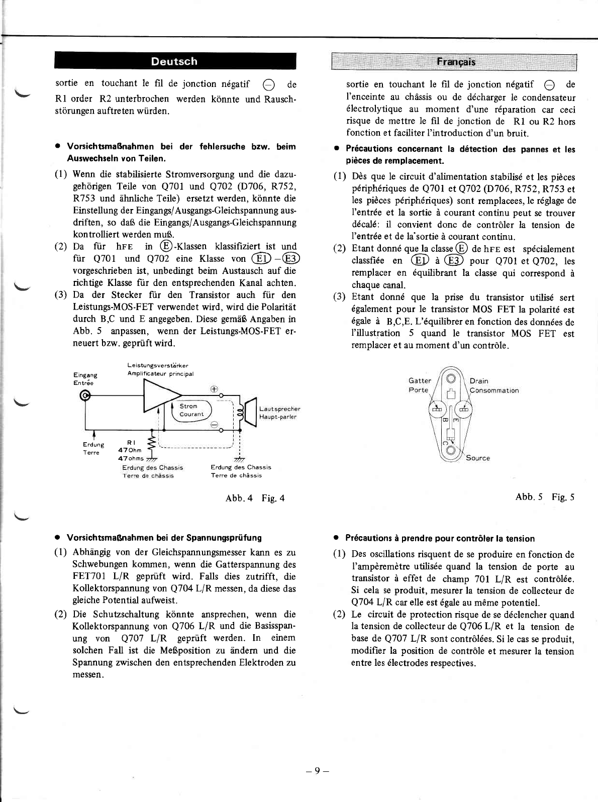
oR1
Die Erdleitung der Signalleitung und die Erdung des
Chassis sind mit Hilfe von Rl (47 Ohm) miteinander
verbunden wie es in Abb. 4 gezeigt ist.
Der Grund dafùr ist der Leistungs-MOS-FET; um
nàmlich die Kapazi6t zwischen dem FET und den Kirhl-
rippen zu erhalten muf3 der FET gegenúber dem Chassis
mit Hilfe eines 47 Ohm Widerstandes isoliert sein.
Daher unbedingt darauf achten, dafJ der negative Q
Leiter des Lautsprechers zum Chassis nicht beri.rhrt wird,
da es ansonsten zu einer Entladung des Elektrolyt-
kondensators kommen kònnte, wodurch der Leiter vor
;
Frs
POINTS DE SERVICE
. Etant donné que cet appareil emploie une importante
capacité d'énergie, faire attention aux points suivants
au moment d'effectuer des contròles et des réparations.
(l) Pour contrÒler et vérifier les plaques ó circuit imprimé,
ne pas oublier de couper I'alimentation et de dé-
brancher le cordon secteur.
Décharger les condensateurs de puissance en les
touchant avec une résistance d'environ 10 ohms,
5 watts de capacité aux points C803 et C804.
Quand une décharge est effectuée par la terre du
chàssis, on peut craindre que le fil de Rl ou R2
provoquent un circuit ouvert et qu'un bruit vienne se
mélanger; si le cas se produit, décharger entre les
bomes positive @ .t négative O du condensateur
électrolytique.
(2) Ne pas toucher les bomes prochent des condensateurs
avec les sondes d'un voltmètre à courant continu au
moment du branchement pour le réglage du courant
déwatté car ceci peut provoquer des détèriorations.
Manipuler délicatement le voltmètre à courant continu.
Isoler la tige du tournevis.
o Procédé de montage des pièces
Prendre soin au montage des pièces pour assurer une
sécurité intégrale à I'appareil. Par exemple, les pièces qui
sont à recouvrir de gaines ou à éloigner des plaquettes à
circuit imprimé. Assurer des conditions optima après
avoir procédé au remplecement de pièees.
Sólecteur Dl RECT COUPLING /CONDENSE R
COUPLING
Etant donné qu'il s'agit là d'un amplificateur à courant
continu quand une fuite de courant continu se produit
dans l'équipement branché à I'entrée, elle sera amplifiée
et une polarisation à courant continu se produit à
I'enceinte ce qui détèriore la qualitésonore et génère des
distorisions; ce sélecteur est prévu pour éviter que cela se
produise.
Il évite également le passage d'un important composant à
courant continu car la panne dans l'amplificateur de
commande risque d'endommager l'enceinte. Sii une fuite
à courant continu se produit dans l'entrée, un bruit
caractéristique ("puu . . .") est audible quand le sélecteur
est réglé sur la position CONDENSER COUPLING au
moment or) cela se produit.
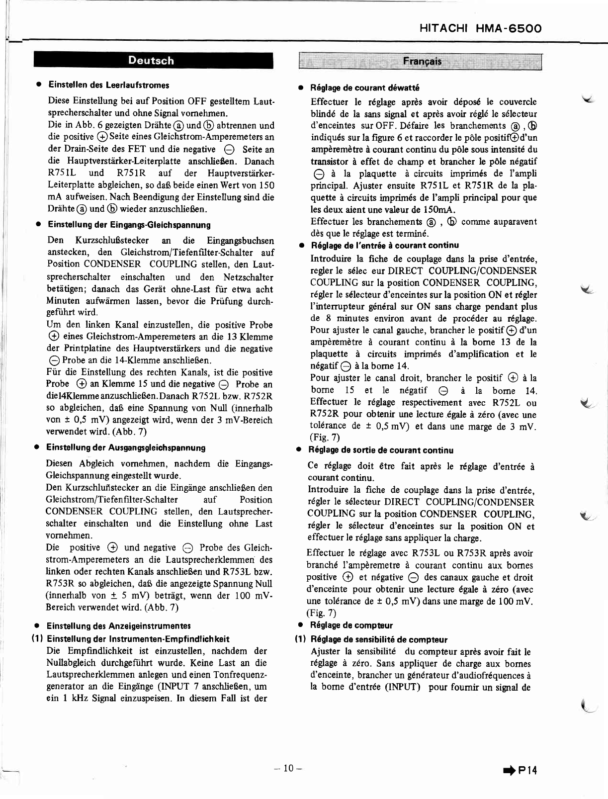
R1
La terre de la ligne de signal et la terre du chàssis de
I'appareil sont connectées à I'aide Rl (47 ohm$
coÍrme le montre l'íllustration 4.
Ceci est dù au fait que le MOS FET d'alimentation est la
source et pour maintenir une capacíté suffisante entre le
transistor à effet de champ et le ventilateur de rayonne-
ment, la stabilité étant détruite par ce cas, le FET est
ainsi isolé du chîssis en employant une résistance de 47
ohms.
Par conséquent, faire attention de ne pas provoquer une
î
î
î
A'
-8-
î

\-
\-
(2)
(3)
sortie en touchant le fil de jonction négatif O de
Rl order R2 unterbrochen werden kónnte und Rausch-
stórungen auftre ten wúrden.
a Vonichtsmaf3nahmen bei der fehlersuche bzw. beim
Auswechseln von Teilen.
(1) Wenn die stabilisierte Stromversorgung und die dazu-
gehórigen Teile von Q701 und Q7O2 (D7O6, R752,
R753 und àhnliche Teile) ersetzt werden, kònnte die
Einstellung der Eingangs/Ausgangs-Gleichspannung aus-
driften, so dafJ die Eingangs/Ausgangs-Gleichspannung
kontrolliert werden mu3.
Da fùr hrp in @-t<lassen klassifiziert ist und
fùr Q701 und Q70i eine Klasse uon @ -@
vorgeschrieben ist, unbedingt beim Austausch auf die
richtige Klasse fiir den entsprechenden Kalal achten.
Da der Stecker firr den Transistor auch fùr den
Leistungs-MOS-FET verwendet wird, wird die Polaritàt
durch B,C und E angegeben. Diese gemàB Angaben in
Abb. 5 anpassen, wenn der Leistungs-MOS-FET er-
neuert bzw. geprùft wird.
E ingang
Entrée
Leistungsverst 'rke.
Amplificateur principal
sortie en touchant le fil de jonction négatif O de
I'enceinte au chàssis ou de décharger le condensateur
électrolytique au moment d'une réparation car ceci
risque de mettre le fil de jonction de Rl ou R2 hors
fonction et faciliter I'introduction d'un bruit.
. Précautions concernant la détection des pannes et les
pièces de remplacement.
(1) Dès que le circuit d'alimentation stabilisé et les pièces
périphériques de Q70l etQ702 (D706, R752, R753 et
les pièces périphériques) sont remplacees, le réglage de
I'entrée et la sortie à courant continu peut se trouver
décalé: il convient donc de contrÒler la tension de
l'entrée et de la'sortie à courant continu.
(2) Etant donné que la clasry@ de hre est spécialement
classfiée en G, à Q!) pour Q70l et Q702, les
remplacer en équilibrant la classe qui correspond à
chaque canal.
(3) Etant donné que la prise du transistor utilisé sert
également pour le transistor MOS FET la polarité est
égale à B,C,E. L'équilibrer en fonction des données de
l'illustration 5 quand le transistor MOS FET est
remplacer et au moment d'un contrÒle.
Abb.5 Fig.5
. Précautions à prendre pour contróler la tension
(1) Des oscillations risquent de se produire en fonction de
I'ampèremètre utilisée quand la tension de porte au
transistor à effet de champ 701 L/R est contrÒlée.
Si cela se produit, mesurer la tension de collecteur de
Q704 L/R car elle est égale au méme potentiel.
(2) Le circuit de protection risque de se déclencher quand
la tension de collecteur de Q706 L/R et la tension de
base de Q707 L/R sont contròlées. Si le cas se produit,
modifier la position de contrÒle et mesurer la tension
entre les électrodes respectives.
Erduns R I
T.... " 47 Ohm
47 ohms Erdung des Chassis
Terre de chàssis
Abb.4 Fig. 4
o VorsichtsmaBnahmen bei der Spannungsprúfung
(1) Abhiingig von der Gleichspannungsmesser kann es zu
Schwebungen kommen, wenn die Gatterspannung des
FET7OI L/R geprùft wird. Falls dies zutrifft, die
Kollektorspannung von Q704 L/R messen, da diese das
gleiche Potential aufweist.
(2) Die Schutzschaltung kónnte ansprechen, wenn die
Kollektorspannung von Q706 L/R und die Basisspan-
ung von Q707 L/R geprùft werden. In einem
solchen Fall ist die Me8position zu àndern und die
Spannung zwischen den entsprechenden Elektroden zu
messen.
-9 -

o Einstellen des Leerlaufstromes
Diese Einstellung bei auf Position OFF gestelltem Laut-
sprecherschalter und ohne Sigral vornehmen.
Die in Abb. 6 gezeigten Driihte @ und @ abtrennen und
die positive @ Seite eines Gleichstrom-Amperemeters an
der Drain-Seite des FET und die negative O Seite an
die Hauptvers6rker-Leiterplatte anschlie8en. Danach
R75lL und R75lR auf der Hauptversfdrker-
Leiterplatte abgleichen, so dafi beide einen Wert von 150
mA aufweisen. Nach Beendigung der Einstellung sind die
Driihte@ und @ wieder anzuschliefien.
o Einstellung der Eingangs-Gleichspannung
Den KurzschluBstecker an die Eingangsbuchsen
anstecken, den Gleichstrom/Tiefenfilter-Schalter auf
Position CONDENSER COUPLING stellen, den Laut-
sprecherschalter einschalten und den Netzschalter
betàtigen; danach das Geràt ohne-Last fùr etwa acht
Minuten aufwàrmen lassen, bevor die Prúfung durch-
gefirhÉ wird.
Um den linken Kanal einzustellen, die positive Probe
@ eines Gleichstrom-Amperemeters an die 13 Klemme
der Printplatine des Hauptverstàrkers und die negative
Q Probe an die l4-Klemme anschliefien,
Fùr die Einstellung des rechten Kanals, ist die positive
Probe @ an Klemme 15 und die negative Q Probe aa
die l4Klemme anzuschlie8en. Danach R7 5 2L bzw. R7 5 2 R
so abgleichen, da$ eine Spannung von Nr.rll (innerhalb
von + 0,5 mV) angezeigt wird, wenn der 3 mV-Bereich
verwendet wird. (Abb. 7)
. Einstellung der Ausgangsgleichspannung
Diesen Abgleich vomehmen, nachdem die Eingangs-
Gleichspannung eingestellt wurde.
Den Kurzschlufstecker an die Eingiinge anschlie$en den
Gleichstrom/Tiefenfilter-Schalter auf Position
CONDENSER COUPLING stellen, den Lautsprecher-
schalter einschalten und die Einstellung ohne Last
vomehmen.
Die positive @ und negative Q Probe des Gleich-
strom-Amperemeters an die Lautsprecherklemmen des
linken oder rechten Kanals anschlieBen und R753L bzw.
R753R so abgleichen, daB die mgezeigte SpannungNull
(innerhalb von * 5 mV) betràgt, wenn der 100 mV-
Bereich verwendet wird. (Abb. 7)
. Einstellung des Anzeigeinstrumentes
(1 I Einstellung der Instrumenten-Empfindlichkeit
Die Empfindlichkeit ist einzustellen, nachdem der
Nullabgleich durchgefiihrt wurde. Keine Last an die
Lautsprecherklemmen anlegen und einen Tonfrequenz-
generator an die Eingànge (IMUT 7 anschlieBen, um
ein I kHz Sigral einzuspeisen. In diesem Fall ist der
HITACHI HMA-6500
o Róglage de courant déwatté
Effectuer le réglage après avoir déposé le couvercle
blindé de la sans sigral et après avoir éf,é le sélecteur
d'enceintes sur OFF. Défaire les branchements @ , (D
indiqués sur la figure 6 et raccorder le pÒle positif@d'un
ampèremètre à courant continu du póle sous intensité du
transistor à effet de champ et brancher le póle négatif
O à lz plaquette à circuits imprimés de I'ampli
principal. Ajuster ensuite R751L et R751R de la pla-
quette à circuits imprimés de I'ampli principal pour que
les deux aient une valeur de 15OmA.
Effectuer les branchements @ , (E comme auparavent
dès que le réglage est terminé.
o Róglage de l'entróe à courant continu
Introduire la fiche de couplage dans la prise d'entrée,
regler le sélec eur DIRECT COUPLING/CONDENSER
COUPLING sur la position CONDENSER COUPLING,
régler le sélecteur d'enceintes sur la position ON et régler
I'intemrpteur général sur ON sans charge pendant plus
de 8 minutes environ avant de procéder au réglage.
Pour ajuster le canal gauche, brancher le positif @ d'un
ampèremètre à courant continu à la bome 13 de la
plaquette à circuits imprimés d'amplification et le
négatif Q àlabome 14.
Pour ajuster le canal droit, brancher le positif @ a U
bome 15 et le négatif O à la bome 14.
Effectuer le réglage respectivement avec R752L ou
R752R pour obtenir une lecture égale à zéro (avec une
tolérance de t 0,5 mV) et dans une marge de 3 mV.
(Fig. 7)
o Réglage de sortie de courant continu
Ce réglage doit étre fait après le réglage d'entrée à
courant continu.
Introduire la fiche de couplage dans la prise d'entrée,
régler le sélecteur DIRECT COUPLING/CONDENSER
COUPLING sur la positíon CONDENSER COUPLING,
régler le sélecteur d'enceintes sur la position ON et
effectuer le réglage sans appliquer la charge.
Effectuer le réglage avec R753L ou R753R après avoir
branché I'ampèremetre à courant continu aux bomes
positive @ et négative Q des canaux gauche et droit
d'enceinte pour obtenir une lecture égale à zéro (avec
une tolérance de + 0,5 mV) dans une mÍuge de 100 mV.
(Fig. 7)
o Réglage de compteur
(1) Réglage de sensibilité de compteur
Ajuster la sensibilité du compteur après avoir fait le
rég7age à zéto. Sans appliquer de charge aux bornes
d'enceinte, brancher un générateur d'audiofréquences à
la bome d'entrée (IMUT) pour foumir un signal de
u_
u,
i
i
ri
I
l
v,
- t0- iPt4

HITACHI HMA-6500
CIRCUIT DIAGRAM.SCHALTPLAN.PLAN DE CIRCUIT
43.O
qforL \
zsc-rz7s€)
06
INPUT - 8
DC odj.
Rch(Some os Lch)
P.W. B.
I
I
INPUT(L )I
eq
NO
EE
Axial lead cylindrical ceramic capacitor
Zylindrischer KeramikkondensatoÌ mit axialer zuleitung
Condensateur céramique cylindrique à conducteur axial
+B
GND
-B
HEADPHONE
PRODUCT SAFETY NOTE: Components marked with a A have special
SICHERHEITSHINWEIS: Die mit A gekennzeichneten Komponentsn haven
NOTICE DE SECURIîE DE FABRICATION; Les composants qui sont
I
I
*
= fÈi
d8 I N
oN+
ù>T
caractéristiquesspóciales. _ ll

J
F>
OO
,î,
1i \P.T.
llil
R952L ml53L
47K rS20
Pow€r supply P.W.B
Ifor U.K only)
îr
Voltoge selslÍ
l:OFF
2 | 24OV
3 | 22OV
4: l20V
sw !-'
I
(for Asio A
act20/
220/ 240V
5Ol60Hz
Power SW
Lolin Americon
counlries )
:T4OA
24OV I
@
@
o
o
@
o
@
o
o
@'
o
c95rL
to/9
SPEAKER SW,
A: OFF
B: SPEAKER A
C: SPEAKER B
POWER METER(L)
+
Meîer
sensiîiviîy odj.
POWER METER(R)
R733L R752L
t&Rct/a<t&Rctzl<
rscteristics important to safety.
r wichti ge Sicherheitsaufgaben.
rmpagnós du symbole A possèdent des
- l1-
(for Europs,Sweden A
(forU.K.a Ausfrolio)
ffifl rcsor BLocK DrAG
SPEAKER B
)NE JACK
o95rR
2SC4580
I
The circuit diagram is subject to change for improvement without notice.
llnderungen des Schaltplans im Sinne stàndiger Verbesserung vorbehalten.
Le schéma de montage est sujet à modification sans préavis, pour des raisons d'amélioration.

ì
PRINTED WIRING BOARD.PRINTPLATTEN.PLAN DE BASE
^ MA|N AMp.HAUPTVERSTARKER.AMpLtF|CATEUR pRtNCtpAL
Inpul lerminol PW.B.
t{t,.
t%t:
^
HEADPHONE jock
MAIN AMP P.W.B.
I I: +B,
A
The terminal No. shows the stamp
board. This number matches the
diagram.
on the printed wiring
number in the circuit Die Anschlussklemmen sind auf der gedruckten Schaltung
numeriert. Die Nummern stimmen mit den Nummern im
Schaltplan úberein.
POWER METE
:^

i-B, I :Earth, :Other
POWER METER(R)
Le No de borne correspond à l'indication de la plaquette à
circuit imprimé. Ce numéro correspond au numéro du
schéma de montage.
HITACHI HMA.6500
: Axial lead cylindrical ceramic capacitor
: Zylindrischer Keramikkondensator mit axialer zuleitiung
: Condensateur céramique cyfndrique à conducteur axial
HAr2002 2SK r33
2SJ48 2SCt775 2SC458
2SB6464 254893
2SD666A 2SCr890
HZ-7
rs2076
HZ-9
HZ-t2 s 5v 820
m*
--t( ^
-Ja ^
R METER(L)

HITACHI HMA.6500
POWER SUPPLY . STROMOUELLE .ALIMENTATION
7\
-
(U.S.A. & Canadal (Australia & U.K.l
-13-
^
(France, W. Germany, Switzerland & Swedenl (Asia & Latin American countries)

FErTOzL Abb. 6
Fig. 6
Eingang so einzustellen, da$ das Instrument fiir den
linken Kanal 1 W anzeigt. R955R so abgleichen, der
das Instrument firr den rechten Kanal 1 W anzeigt
(Abb.7).
KONTROLLE DER FUNKTION
DEFI SCHUTZSCHALTUNG
Falls die Ausgangsschaltung repariert wurde, indem z.b.
die Leistungs-MOS-FET usw. erneuert wurden, dann
muB die . ASO-Schutzschaltung (ASO = Area of Safe
Operation) und die Lautsprecher-Schutzschaltung
kontroliert werden.
1 Funktionsprúfung der ASO-Schaltung fiir die Leistungs-
MOS-FET
Den Frequenzoszillator an die Eingangsklemmen
INPUT) anschlie8en, wobei die Lautsprecherklem-
men keine Last aufiveisen dùrfen (Lautsprecher nicht
angeschlossen). lie Frequenz des Frequenzosziliators
auf I kllz einstellen und den Pegel des Eingangssi-
gnales so abgleichen, daf3 die Spannung an den Laut-
sprecherklemmen etwa 5V (Mittelwert, beutertet) be-
tràgt. In diesem Zustand sind die Lautsprecherklem-
men kurzzuschliefien, und zwar die Klemmen jenes
Kanals, an welchen das Eingangssignal angelegt wurde.
Falls dieser Kurzschluff zu einem Ansprechen der ASO-
Schutzschaltung fúhrt, durn erscheint kein Ausgangs-
signal an den Lautsprecherklemmen, auch nicht wenn
den zum Kurzschlieffen der Klemmen verwendete Draht
entfemt wird.
Danach den Netzschalter abschalten und nach etwa 10
Sekunden wieder einschalten. Wenn nun ein Ausgangs-
signal an den Lautsprecherklemmen festgestellt wird
bedeutet dies, dafJ die ASO-Schutzschaltung richtig
arbeitet.
2 Funktionsprùfung der Lautsprecher-Schutzschaltung
Darauf achten, dafi etwa 4 Sekunden nach dem Ein-
schalten des Netzschalters ein Schaltgeràusch des Re-
lais vernommen werden kann, wenn keine Last an den
Lautsprecherklemmen anliegt (Lautsprecher nicht an-
gesctrlossen).
Danach einen Widerstand mit etwa l0 kOhm und 2
Trockenbatterien (1,5V) in Serie mit der R902 auf
der Schaltplatine und der Úberbrúckung @ , wonach
:; i1
Abb. 7
Fig. 7
I kHz. Dans ce cas, ajuster I'entérée de sorte que I'ai-
guille du canal gauche indique lW.
Ajuster R955R pour que I'aiguille du canal droit
indique lW (Fig. 7).
CONTROLE
DU CIRCUIT DE FONCTTONNEMENT{\
DE PROTECTION
i
rl
I
l
il
Quand le circuit de sortie est réparé à la suite du rem-
placement des transistors à effet de champ, etc, effectuer
une vérification de fonctionnement du circuit de détection
de type ASO et du circuit de protection de haut-parleur.
1 Contròle de fonctionnement du circuit de détection de
type ASO pour les transistors a effet de champ
Brancher un oscillateur d'onde sonore aux bornes î\
d'entrée quand aucune charge n'est appliquée aux
bomes de haut-parleur (haut-parleur débranché).
Régler la fréquence de I'oscillateur d'onde sonore à
I kHz et ajuster le niveau du signal d'entrée de telle
sorte que la tension appliquée aux bornes de haut-
parleur soit environ de 5V efficace. Quand ces con-
ditions sont obtenues, court-circuiter les bomes de
haut-parleur du canal recevant le sigrral d'entrée en se
servant d'un fil de jonction, etc. Si le court-circuit met
le circuit de détection de type ASO en fonction,
aucune sortie n'est relevée aux bomes de haut-parleur
méme si le fil de jonction utilisé pourle court-circuitage
est retiré.
Ensuite, mettre I'interrupteur général à l'arrét et après
un délais approximatif de 10 secondes, le mettre à
nouveau en fonction. Quand la sortie parvient aux
bomes de haut-parleur, c'est le signe que le circuit de
détection de type ASO fonctionne normalement.
2 Contróle de fonctionnement du circuit de protection
de haut-parleur
S'assurer que le relais fonctionne (un déclic se produit)
environ 4 secondes après la mise en fonction de I'inter-
rupteur général quand les bomes de haut-parleur ne
regoivent aucune charge (haut-parleur débranché).
Ensuite, quand une résistance d'environ 10k-ohms
d'impédance et 2 piles sèches (1,5V) sont branchées en
série à R902 de la plaquette à circuit imprimé audio et
le cavalier @ ,t" relais se met hors fonction en moins
.s\
FEÎ7O2R
14-
A\

das Relais innerhalb einer Sekunde Abschalten sollte.
Werden die Trockenbatterien wieder entfernt, dann
arbeitet das Relais wiederum. Anschliefiend die Polaritàt
der Trockenbatterien umpolen und die obige Prùfung
des Relais nochmals durchfuhren. Wenn auch nun das
Relais aktiviert wird, dann ist die Lautsprecher-
Schutzschaltung in Ordnung. Bei dieser Prùfung ist
besonders darauf zu achten, da$ keine der benachbarten
Teile kurzgeschlossen we rden.
HITACHI HMA.6500
d'une seconde. Quand les piles sèches sont retirés le
relais se remet une nouvelle fois en fonction.
Ensuite, modifier les polarités des piles sèches et pro-
céder au contrÒle précédemment décrit pour s'assurer
que le fonctionnement du relais est normal. Si ces
conditions permettent au relais de se mettre en fonc-
tion, cela veut dire que le circuit de protection de haut-
parleur fonctionne normalement. Par ailleurs, faire
attention de ne pas court-circuiter les pièces et composants
avoisinants au cours de ce contrOle.
Abb.9
Fig. 9
Procédé de contròle du MOS FET d'alimentation
Déposer le transistor a effet de champ, Quand il s'agit d'un
canal N FET, il est normal: qu'au moment de toucher avec
la sonde de contrÒle noire du contr6leur, le drain du FET et
avec la sonde de eontróle rouge (gamme ohms) à la souree
en méme temps et après avoir appliqué la sonde de contróle
noire à la porte et la sonde de contrÒle, rouge à la source,
qu'un courant passe. Ensuite, quand la porte et la source
sont touchées en méme temps avec les mains, le courant est
interrompu.
S'il s'agit du canal P, les sondes de contròle rouge et noire
du contrÓleur sont appliquées en position inverse.
^^
^
7
Fre quenzgenero îor Wechse lsî rom - Voltmeler
Oscilloîeur Voltmèîre ù couronf
dtondè sonore
Osz i I logroph
oscil loscope
Abb. 8
Fig. 8
fverfahren fùr Leistungs-MOS-FET
Den FET ausbauen, Im Falle eines N-Kanal Feldeffekt-
transistors ist es normal, daB ein Strom flieflt, wenn die
schwarze Prùfprobe des Prúfgeràtes an den Drain des FET
und die rote Prùfprobe (Ohm-Bereich) an die Source
angelegt wird, nachdem die Schwarze Probe an das Gatter
angelegt wurden. Wenn Sie danach gleichzeitig das Gatter
und die Source mit lhrer Hand reiben, wird der StromflufJ
unterbrochen.
Im Falle eines P-Kanal Transistors mùssen die rote und die
schwarze Prùfprobe umgekehrt angelegt werden.
1^
- 15 -

HITACHI HMA-6500
3. AnschluBmóglichkeiten fùr zwei Paar Laut-
sprecher
An diesen Verstàrker kónnen zwei Lautsprecher
paare angeschlossen werden Mit dem Laut
sprecherschalter kònnen die Paare einzeln ein-
geschaltet werden, und so kònnen Sie die
Klangreproduktion ledes Paars vergleichen.
Selbstverstandlich ist es auch mòglich, die
Lautsprecherpaare in verschjedenen Zlmmern
aufzustellen, um so die Wiedergabe zu horen.
4. Zuverlàssige Schutzschaltung
Zum Schutz der POWER MOS FET-Lerstungs-
stufe sind eine Stromspiegelschaltung und eine
Gleichspannungsnachweisschaltung eingebaut.
Dieser Schaltkreis bes,itzt eine hohe ZuverlAssig-
keit bei auftretenden Stòrungen.
CARACTERISTIQUES
HITACHI a développé un condensateur à effet de champ (MOS FET) complémentaire qui se distingue par des
caractéristiques superbes en tant que dispositif d'amplification de puissance pour des applications audio. Comme,
à la fois, les caracîéristiques canal-N et canal-P de ce POWER MOS FET sont d'une clase supérieure, ce modèle
se distingue par une configuration simple d'un circuit 3-étages y compris l'étage d'amplification. Ceci constitue un tì
dispositif qui permet d'obtenir un niveau de distorsion très bas tout le long d'une bande très large et qui est
destiné à produire la meilleure ingéniérie pour une qualité de son supérieure.
5. GroRe Leistungspegelmesser
(Spitzenpegelmesser)
Dieses Modell ist mit groBen Leistungspegel-
messern ausgerústet, die eine genaue Balance
zwischen linkem und rechtem Kanal sowie
eine Kontrolle des Ausgangspegels ermóglichen.
lhre GróBe und Leistung sind so bemessen wie
man es bei einem Verstarker mit POWER MOS
FET-Leistungsendstufe der Spitzenklasse er-
warten kann. Die Leistungspegelmesser slnd mit
elner logarithmischen Dynamikregelschaltung
ausgestattet und zeigen den Effektivwert (RIVS)
des Spitzenpegels an. Dies bedeutet, daB sie
Spitzenimpulssignale pràzise anzeigen und jeder-
zeit direkt abgelesen werden kònnen
1. Une conception destinée à obtenir une faible
distorsion tout le long d'une bande très large
pour une qualité sonore supérieure
Le POWER N/OS FET' se caractérise par une
impédance élevée d'entrée et constiîue un
dispositif d'entraînement de tension. Ces deux
avantages permettent d'obtenir un gain de puis-
sance très élevé et une conf iguration de circuit
de conception simple. Voilà pourquoi ie niveau
de bruit parasite est réduit à son minimum ainsi
que le glissement de phase, deux phénomènes
qui exercent un effet nuisible sur la qualité
sonore. Voilà pourquoi, aussi, il n'y aucune
détérioration en ce qui concerne le facteur de
distorsion. En plus, la réponse en fréquence est
excellente, la vitesse de commutation est rapide,
et on est assuré d'un fonctionnenrent stable
méme dans le domaine des hautes fréquences
avec une distorsion de cran réduite de facon
remarquable. Cette conception permet d'ob-
tenir un très bas facteur de distorsion tout le
long d'une vaste bande avec un débit de puis-
sance continu de 50 watts minimum par canal
sous 8 ohms (20 Hz-2O kHz) avec une distor-
sion harmonique totale ne depassant pasO,O2o/o
2. Amplificateur à courant continu se carac-
térisant par une transmission de puissance en
forme d'onde précise
Dans cet amplificateur à courant continu, les
condensateurs ont été éliminés de la boucle
NFB en méme temps que ceux d'entrée, ce qui
permet d'obtenir une remarquable amélioration
des caractéristiques de phase dans le domaine
des basses fréquences. Le premier étage utilise
des transistors à faible bruit parasite et à
résistance élevée à la tension, et se distingue par
des caractéristiques d'accouplement très précises
pour une réduction du niveau du glissement au
point central.
En plus, il y a un commutateur de couplage
direct/couplage par condensateur (DIRECT
COUPLI NG/CONDENSER COUPtING) qui est
installé pour préserver les enceintes des domma-
ges pouvant étre provoqués par une fuite de
courant continu d'un composant en provenance
d'un appareil raccordé extérieurement (tel que
l'amplif icateur de contrÒle).
3. Système de branchement pour deux paires
d'enceintes
On peut relier deux paires d'enceintes à cet am-
plif icateur et l'on peut comparer le son produit
par chaque système en utÌlisant le commutateur
d'ence intes
ll est également possible d'écouter le son
provenant d'un système d'enceìntes dans une
pièce eÌ le son provenant de l'autre système
dans une autre pièce
4. Circuit de protection à haute fiabilité
Dans le but de protéger eff icacement le POWER
N/OS FET, un circuit à miroir courant quì per-
met de déterminer l'espace de fonctionnement
de sécurité, et un circuit de détection de ten-
sion à courant continu, ont été installés. Ces
circuits se caractérisent par un niveau de
fìabilÌte élevé qui permeÌ de protéger efficace-
ment l'appareìllage et de faìre face aux inci-
dents éventuels.
5. lndicateurs de puissance de grande dimension
(indicateurs de crétel
L'appareil est équipé d'indicateurs de puìssance
de grande dimension qui permettent d'obtenir
un équilibrage parfait entre Ies canaux gauche
et droit et également de contrÓler le niveau de
sortie. Leurs tailles et leurs performances sont
celles que vous étes en droit d'attendre d'un
amplificateur de POWER N/IOS FET. Les indi-
cateurs de puissance utìlisent un circult de com-
pression logarithmique pour les affichages de
valeur efficace des crétes détectées. Voici pour-
quoi ils peuvent indiquer lessignaux de créte et
rendre les valeurs affichees directement lisibles.
tl
-18-

-I
ìq
I
BLOGK DIAGRAM.BLOGK SC.HEMA.SCHEMA
HITACHI HMA.6500
Meter lamp
1 st stage Current mirror
A class
differential amp.
Operation
range limiting
protection
crrcutt
I
POWER
MOS FET
DrREcrcoupLrNG/ differential
coNDENSER couÈrt ruG amP' +82
INPUT
(1 Vl
AC 120 V 6O Hz
_12OVl22OVl24OV, power
50/6O Hz sw'
+Bl
,A
n
+12 V
Stabi lized
power
soufce
tB2
-82
Speaker relay
drive, Muting,
DC detection
ctrcurt
UNSWITCHED
4OOW MAX.
(for U.S.A., Canada, Asia
& Latin American countriesl
n
+B I
-82' +-B I
^
-19-

HITACHI HMA-6500
REPLACEMENT PARTS LIST.ERSATZTEILLISTE.TABLEAU DES PIECE
SYMBOL
NO. STOCK
NO. DESCRIPTION SYMBOL
NO. STOCK
NO. DESCRIPTION
CAPACITORS R733(L,R)
R734
R738(L,R)
R73e(L,R)
R74 r
Res r (L,R)
R9s2(L,R)
Re53(L,R)
R9s4(L,R)
R955 L
RT
R90 r
R902
R903
R90 5
R906
R90 7
R908
R909
H134362
}{tt42al
Htt4281
H1143r 1
Hlt42r3
Hlt422t
Hlt422t
Hrt4223
H I 34380
11r9545
H114281
Htt428l
lll963r
Hl1420t
Hrt4r71
Hl14r35
I{tt420l
}{tt4t49
o134291
Composition
Carbon film
Carbon film
Carbon film
Carbon film
Carbon film
Carbon film
Carbon film
Composition
Metal oxide
Composition
Carbon film
Metal oxide
Carbon film
Carbon film
Carbon film
Carbon film
Carbon film
Composition
3.9kO + lOVo
2.2k{t +to%
l00kQ +5%
r00kf,l +s%
ó80st +to%
rOko xs%
4.1klt !s%
150S' +5%
10ko +s%
s60l, +5%
47dl +lo%a
120f,l LlÙlo
l00ko +s%
1 80ko
lMO
33ksl
ó8ko
6 8ko
82ko
+s%
!s%
+s%
+s%
!s%
!s%
RC%GF
SRD/rP
SRD%P
SRD/aP
SRDT+P
SRD/rP
SRD%P
SRD/rP
RC%GF
R52PA
SRDTcP
SRD/+P
RS3PA
SRD/rP
SRD/rP
SRD/rP
SRD%P
SRD/rP
RC%GF
for
c70 r (L,R)
c702(L,R)
c7o3(L,R)
c704(L,R)
cTos (L,R)
c7o6(L,R)
c7o8(L,R)
cToe(L, R)
c7r0
c1t I
c't t2
c?r3
c1t4
c80 1
c 802
c80 3
c804
c90 I
c903
c904
c90 5
c906
ce s 1 (L,R)
ces2(L,R)
IAIN AMP
t252at I
H23003ó
o241as4
02192ll
0247 802
0247802
o2192t I
o257 145
r252s2t
t252527
1252521
LIFIER PRINT
Electroly tic
Ceramic, discal
Ceramic, discal
Mylar, film
Ceramic, discal
Ceramic, discal
Mylar, film
Electrolytic
Electrolytic
Electrolytic
Electrolytic
Mylar, film
Mylar, frlm
Ceramic, discal
Ceramic, discal
Electrolytic
Electroly tic
Electrolytic
Electrolytic
Electrolytic
Electrolytic
Electrolytic
Electrolytic
Electrolytic
D WIRING BOA
l/iF
100pF ts%
1oopF rs%
o.l/lF rto%
2pF t0.25pF
2pF t0.25pF
0.lpF Lto%
10pF
I opF
10pF
I OpF
0.l/.rF LrO%
0.lpF LtO%
0.0lpF rzo%
0.0rpF +2O%
I 0,0O0pF
I 0,000pF
22OpF
l0pF
10pF
100lrF
rpF
I OtiF
lpF
ID
s0v
50v
500v
2 50V
500v
500v
2s0v
l6V
16V
t6V
16V
s0v
50v
soov
500v
50v
s0v
ó.3V
16V
l6v
ó.3V
50v
s0v
50V
FETS. lCs & TRANSISTORS
for l!
IC9O l
Q701(L,R)
Q7o2(L,R)
Q703(L,R)
Q7o4(L,R)
QTos(L,R)
Q706(L,R)
Q70 7
Qes l(L,R)
FETTO I
(L,R)
FET7O2
(L,R)
IAIN AMP
2361372
2328612
2324612
2328454
2324458
IFIER PRINTED WIRING BOARD
HA12002
2SCl77s Qoó
2sc17?s (E) 06
2sB646A Ó o l
258646A @ or
2SDóó6A Q 0 l
2sc I 8eoJE)
2sA8e3 (E)
2Sc4s8 o
2sK133
2SJ48
RESISTORS
for l!
R?01(L,R)
R702 (L, R)
R7o3(L,R)
R704(L,R)
R?0s(L,R)
R70ó(L,R)
R707(L,R)
R708(L,R)
RToe(L,R)
R71o(L,R)
R7l r(L,R)
R? r 2(L,R)
R713(L,R)
R714(L,R)
R71 s (L,R)
R718(L,R)
RT l e (L,R)
R720
R72r (L,R)
R723(L,R)
R724(L,R)
R72 s (L,R)
R72 6(L,R)
R72 7(L,R)
R728
R729
R730
R73 I
R732 (L, R)
Hl 14169
Hr 14303
H114169
Htt42t9
Ht1420t
Htt4l13
H114173
H114165
H114139
Htt4201
Hr 14131
Hl14133
H 114131
Hl14145
Htt42t3
Hlt42t1
Htt4t77
Hrt4l69
Hr29509
1r19135
Htl4295
Htt42t7
HlL42l7
Htt4291
H134380
Hr 34380
Htt4223
Htt4r79
H134362
Carbon film
Carbon film
Carbon film
Carbon film
Carbon film
Carbon film
Carbon film
Carbon film
Carbon film
Carbon filrn
Carbon film
Carbon film
Carbon film
Carbon film
Carbon frlm
Carbon film
Carbon frlm
Carbon film
Carbon film
Metal
Carbon film
Carbon film
Carbon film
Carbon film
Composition
Composition
Carbon frlm
Carbon frlm
Composition
IAIN AMPLIFIER PRINTED WIRING BOA
2.2kdt ts%
82oko rs%
2.2kdù ts%
s6ko rs%
rokQ Ls%
3.3kO rs%
3.3kO rs%
r.sko +s%
22Ùdl tSVo
l8ko r.s%
100st +5%
r20o rs%
r00,Q +s%
390Q +s%
33kS' Ls%
47k0 +s%
4.7k,Q + s%
2.2kdl + s%
2.2d1 + s%
2.2d1 + tOVo
390k0 +s%
47ktr +5%
4?kA +5%
4?0kS, +5%
3.9ks, +5%
3.9ksr !s%
82kQ Ls%
s.6ko Ls%
r20tÌ +to%
D
SRDYaP
SRD/rP
SRD%P
SRD/rP
SRD%P
SRD/aP
SRD%P
SRD%P
SRD/+P
SRD%P
SRDY"P
SRD/cP
SRD%P
SRD/rP
SRDi;P
SRD/rP
SRDTaP
SRD%P
SRD%P
RN2B
SRD/rP
SRD/rP
SRD/rP
SRD/rP
RC%GF
RC%GF
SRD%P
SRDTeP
RC%GF
DIODES
for
D?o 1(L,R)
D?02(L,R)
D7o3(L,R)
D?04(L,R)
D70s (L,R)
D?06(L,R)
D801
D90r
D902
D9s 1(L,R)
Des 2(L,R)
Des3(L,R)
D954(L,R)
IAIN AMP LIFIER PRINTED WIRING BOARD
Table of contents
Other Hitachi Amplifier manuals

Hitachi
Hitachi IA-1200 User manual

Hitachi
Hitachi HCA-6500 User manual

Hitachi
Hitachi HA-6800 User manual

Hitachi
Hitachi HTA-12 User manual

Hitachi
Hitachi HA-5300 User manual

Hitachi
Hitachi HA-7700 User manual

Hitachi
Hitachi HMA-750 MK2 User manual

Hitachi
Hitachi HCA-8500Mk2 User manual

Hitachi
Hitachi HA-7700 User manual

Hitachi
Hitachi HA-M33 User manual

Hitachi
Hitachi HMA-8300 User manual

Hitachi
Hitachi HA-2800 User manual

Hitachi
Hitachi HA-M44 User manual

Hitachi
Hitachi HMA-7500 User manual

Hitachi
Hitachi HA-3700 User manual

Hitachi
Hitachi HA-330 User manual

Hitachi
Hitachi HA-5700 User manual

Hitachi
Hitachi HTA-4000 User manual

Hitachi
Hitachi HMA-8300 User manual

Hitachi
Hitachi HCA-7500 User manual