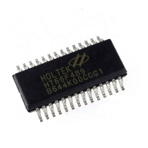
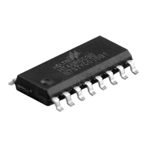
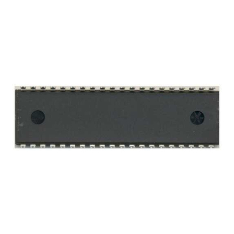
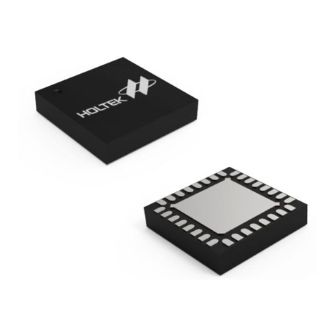
Holtek HT46R74D-1 Technical manual

HT46R74D-1
Dual Slope A/D Type MCU with LCD
Rev. 1.40 1 January 10, 2008
Features
·Operating voltage:
fSYS = 4MHz: 2.2V~5.5V
fSYS = 8MHz: 3.3V~5.5V
·10 bidirectional I/O lines and two ADC inputs
·Two external interrupts inputs shared with I/O lines
·One 8-bit and one 18-bit programmable timer/event
counter with overflow interrupt and pre-scaler
·LCD driver with 15´4, 16´3or16´2 segments
·4K´15 program memory with partial lock function
·96´8 data memory RAM
·Single differential input channel dual slope Analog to
Digital Converter with Operational Amplifier.
·Watchdog Timer with regulator power
·Buzzer output
·External 32768Hz RTC oscillator
·Integrated RC or crystal oscillator
·Power-down and wake-up functions reduce power
consumption
·Internal 3.3V Voltage regulator and charge pump
·Embedded voltage reference generator - 1.5V
·6-level subroutine nesting
·Bit manipulation instruction
·15-bit table read instruction
·Up to 0.5ms instruction cycle with 8MHz system clock
at VDD=5V
·63 powerful instructions
·All instructions in 1 or 2 machine cycles
·Low voltage reset/detector function
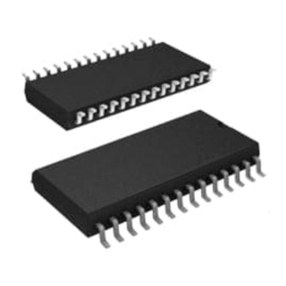
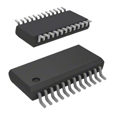
·56-pin SSOP package
General Description
The HT46R74D-1 is an 8-bit high performance, RISC
architecture microcontroller device specifically de-
signed for A/D with LCD applications that interface di-
rectly to analog signals, such as those from sensors.
The advantages of low power consumption, I/O flexibil-
ity, timer functions, oscillator options, Dual slope A/D
converter, LCD display, HALT and wake-up functions,
watchdog timer, as well as low cost, enhance the versa-
tility of these devices to suit for a wide range of AD with
LCD application possibilities such as sensor signal pro-
cessing, scales, consumer products, subsystem con-
trollers, etc.
Technical Document
·Tools Information
·FAQs
·Application Note

Block Diagram
Pin Assignment
HT46R74D-1
Rev. 1.40 2 January 10, 2008
P r o g r a m
C o u n t e r
P r o g r a m
R O M
I n s t r u c t i o n
R e g i s t e r
I n s t r u c t i o n
D ecoder
T i m i n g
G e n e r a t i o n
O S C 2 O S C 1
R E S
V D D
V S S
I n t e r r u p t
C i r c u i t
I N T C
M P MUX
M U X
D a t a
M e m o r
A L U
S h i f t e r
S T A T U S
A C C
S T A C K
B P
H A L T E N / D I S
L V D / L V R
P A
P A C
P B
P B C P o r t B
P o r t A
P B 0 ~ P B 1
P A 0 / B Z
P A 1 / B Z
P A 2
P A 3 / P F D
P A 4 / T M R 0
P A 5 / T M R 1
P A 6 / I N T 0
P A 7 / I N T 1
L C D
M e m o r
L C D D r i v e r
C O M 0 ~ C O M 2
C O M 3 / S E G 1 5
S E G 0 ~ S E G 1 4
C h a r g e
P u m p
R e g u l a t o r
V O R E G
V O C H P
V D D
1-C hannel
D u a l - S l o p e
C o n v e r t e r
w i t h O P
W D T
W D T
P r e s c a l e r
MUX
W D T O S C
R T C O S C
fS Y S / 4
T M R 0 C
T M R 0
MUX
T M R 1 C
T M R 1
MUX
P F D 0
P F D 1
fS Y S / 4
fS Y S
P r e s c a l e r
P A 4 / T M R 0
32768H z
P A 5 / T M R 1
D O P A P
D O P A N
D O P A O
D C H O P
D S R R
D S R C
D S C C
O S C 3
O S C 4
P A 2
P A 3 / P F D
P A 4 / T M R 0
P A 5 / T M R 1
P A 6 / I N T 0
P A 7 / I N T 1
V S S
V D D
A V D D
V O B G P
C H P C 2
C H P C 1
V O C H P
V O R E G
A V S S
D O P A P
D O P A N
D O P A O
DCHOP
D S R R
D S R C
D S C C
P B 0
P B 1
V L C D
V M A X
V 1
V 2
P A 1 / B Z
P A 0 / B Z
R E S
O S C 1
O S C 2
O S C 4
O S C 3
S E G 0
S E G 1
S E G 2
S E G 3
S E G 4
S E G 5
S E G 6
S E G 7
S E G 8
S E G 9
S E G 1 0
S E G 1 1
S E G 1 2
S E G 1 3
S E G 1 4
S E G 1 5 / C O M 3
C O M 2
C O M 1
C O M 0
C 2
C 1
5 6
5 5
5 4
5 3
5 2
5 1
5 0
4 9
4 8
4 7
4 6
4 5
4 4
4 3
4 2
4 1
4 0
3 9
3 8
3 7
3 6
3 5
3 4
3 3
3 2
3 1
3 0
2 9
1
2
3
4
5
6
7
8
9
1 0
1 1
1 2
1 3
1 4
1 5
1 6
1 7
1 8
1 9
2 0
2 1
2 2
2 3
2 4
2 5
2 6
2 7
2 8
H T 4 6 R 7 4 D - 1
5 6 S S O P - A

Pin Description
Pin Name I/O Options Description
PA0/BZ
PA1/BZ
PA2
PA3/PFD
PA4/TMR0
PA5/TMR1
PA6/INT0
PA7/INT1
I/O
Wake-up
Pull-high
Buzzer
PFD
Bidirectional 8-bit input/output port. Each individual pin on this port can
be configured as a wake-up input by a configuration option. Software in-
structions determine if the pin is a CMOS output or Schmitt trigger input.
Configuration options determine which pins on this port have pull-high re-
sistors. The BZ/BZ, PFD, TMR0/TMR1, INT0/INT1 are pin-shared with
PA0/1, PA3, PA4/5, and PA6/7, respectively.
PB0~PB1 I/O Pull-high
Bidirectional 2-bit input/output port. Software instructions determine if the
pin is a CMOS output or Schmitt trigger input. Configuration options de-
termine which pins on this port have pull-high resistors.
VLCD ¾¾
LCD power supply
VMAX ¾¾
IC maximum voltage. Connect to VDD, VLCD or V1
V1, V2, C1, C2 ¾¾
LCD voltage pump
COM0~COM2
COM3/SEG15 O1/2, 1/3 or 1/4
Duty
COM0~COM3 are the LCD common outputs. A configuration option se-
lects the LCD duty-cycle. When either 1/3 or 1/2 duty is selected, the
COM3/SEG15 pin will be configured as SEG15.
SEG0~SEG14 O Segment
Output LCD driver outputs for the LCD panel segments.
VOBGP AO ¾Band gap voltage output pin. (for internal use)
VOREG O ¾Regulator output - 3.3V
VOCHP O ¾Charge pump output - requires external capacitor
CHPC1 ¾¾
Charge pump capacitor, positive
CHPC2 ¾¾
Charge pump capacitor, negative
DOPAN,
DOPAP,
DOPAO,
DCHOP
AI/AO ¾
Dual Slope converter pre-stage OPA related pins. DOPAN is the OPA
Negative input pin, DOPAP is the OPA Positive input pin, DOPAO is the
OPA output pin and DCHOP is the OPA Chopper pins.
DSRR,
DSRC,
DSCC
AI/AO ¾
Dual slope AD converter main function RC circuit. DSRR is the input or
reference signal, DSRC is the Integrator negative input, and DSCC is the
comparator negative input.
OSC1
OSC2
I
OCrystal or RC
OSC1, OSC2 are connected to an external RC network or crystal for the
internal system clock. The OSC2 pin can be used to monitor the system
clock at 1/4 frequency.
OSC3
OSC4
I
O
RTC or
System Clock
OSC3, OSC4 are connected to a 32768Hz crystal to form a real time
clock for timing purposes or to form a system clock.
RES I¾Schmitt trigger reset input, active low
VDD ¾¾
Positive power supply
VSS ¾¾
Negative power supply, ground
AVDD ¾¾
Analog positive power supply
AVSS ¾¾
Analog negative power supply, ground
HT46R74D-1
Rev. 1.40 3 January 10, 2008

Absolute Maximum Ratings
Supply Voltage ...........................VSS-0.3V to VSS+6.0V Storage Temperature ............................-50°Cto125°C
Input Voltage..............................VSS-0.3V to VDD+0.3V Operating Temperature...........................-40°Cto85°C
IOL Total ..............................................................150mA IOH Total............................................................-100mA
Total Power Dissipation .....................................500mW
Note: These are stress ratings only. Stresses exceeding the range specified under ²Absolute Maximum Ratings²may
cause substantial damage to the device. Functional operation of this device at other conditions beyond those listed
in the specification is not implied and prolonged exposure to extreme conditions may affect device reliability.
D.C. Characteristics Ta=25°C
Symbol Parameter Test Conditions Min. Typ. Max. Unit
VDD Conditions
VDD Operating Voltage ¾fSYS=4MHz 2.2 ¾5.5 V
¾fSYS=8MHz 3.3 ¾5.5 V
IDD1 Operating Current (Crystal OSC)
3V No load, fSYS=4MHz
Analog block off
¾0.6 1.6 mA
5V ¾24mA
IDD2 Operating Current (RC OSC)
3V No load, fSYS=4MHz
Analog block off
¾0.8 1.5 mA
5V ¾2.5 4 mA
IDD3 Operating Current (RC OSC) 5V No load, fSYS=8MHz
Analog block off ¾48mA
IDD4 Operating Current (Crystal OSC) 5V No load, fSYS=8MHz
Analog block off ¾48mA
IDD5 Operating Current (RTC OSC)
3V No load, fSYS=32768Hz ¾0.3 0.6 mA
5V ¾0.6 1 mA
IDD6 Operating Current (ADC On) 5V
VREGO=3.3V, fSYS=4MHz
ADC on, ADCCLK=125kHz
(all other analog devices off)
¾35mA
ISTB1 Standby Current (*fS=fSYS/4) 3V No load, system HALT,
Analog block off, LCD off
¾¾ 1mA
5V ¾¾ 2mA
ISTB2
Standby Current
(*fS=RTC OSC)
3V No load, system HALT,
Analog block off, LCD off
¾2.5 5 mA
5V ¾10 20 mA
ISTB3
Standby Current
(*fS=WDT OSC)
3V No load, system HALT,
Analog block off, LCD off
¾25
mA
5V ¾610
mA
ISTB4
Standby Current
(*fS=RTC OSC)
3V No load, system HALT,
Analog block off, LCD on
1/2 bias, VLCD=VDD
(Low bias current option)
¾17 30 mA
5V ¾34 60 mA
ISTB5
Standby Current
(*fS=RTC OSC)
3V No load, system HALT,
Analog block off, LCD on
1/3 bias, VLCD=VDD
(Low bias current option)
¾13 25 mA
5V ¾28 50 mA
ISTB6
Standby Current
(*fS=WDT OSC)
3V No load, system HALT,
Analog block off, LCD on
1/2 bias, VLCD=VDD
¾14 25 mA
5V ¾26 50 mA
ISTB7
Standby Current
(*fS=WDT OSC)
3V No load, system HALT,
Analog block off, LCD on
1/3 bias, VLCD=VDD
¾10 20 mA
5V ¾19 40 mA
HT46R74D-1
Rev. 1.40 4 January 10, 2008

Symbol Parameter Test Conditions Min. Typ. Max. Unit
VDD Conditions
VIL1 Input Low Voltage for I/O Ports,
TMR and INT ¾¾ 0¾0.3VDD V
VIH1 Input High Voltage for I/O Ports,
TMR and INT ¾¾
0.7VDD ¾VDD V
VIL2 Input Low Voltage (RES) ¾¾ 0¾0.4VDD V
VIH2 Input High Voltage (RES) ¾¾
0.9VDD ¾VDD V
VLCD LCD Highest Voltage ¾¾ 0¾VDD V
VLVR1 Low Voltage Reset 1 ¾LVR option= 2.2V 2.1 2.2 2.3 V
VLVR2 Low Voltage Reset 2 ¾LVR option= 3.3V 3.15 3.3 3.45 V
VLVD1 Low Voltage Detector 1 ¾LVR option= 2.2V,
LVD option= LVR+0.2 2.25 2.4 2.55 V
VLVD2 Low Voltage Detector 2 ¾LVR option=3.3V
LVD option= LVR+0.2 3.45 3.6 3.75 V
IOL1 I/O Port Segment Logic Output
Sink Current
3V VOL=0.1VDD
48 ¾mA
5V 10 20 ¾mA
IOH1 I/O Port Segment Logic Output
Source Current
3V VOH=0.9VDD
-2-4¾mA
5V -5-10 ¾mA
IOL2 LCD Common and Segment
Current
3V VOL=0.1VDD
210 420 ¾mA
5V 350 700 ¾mA
IOH2 LCD Common and Segment
Current
3V VOH=0.9VDD
-80 -160 ¾mA
5V -180 -360 ¾mA
RPH Pull-high Resistance of I/O Ports
and INT
3V ¾20 60 100 kW
5V ¾10 30 50 kW
Charge Pump and Regulator
VCHPI Input Voltage ¾Charge pump on 2.2 ¾3.6 V
Charge pump off 3.7 ¾5.5 V
VREGO Output Voltage ¾No load 3 3.3 3.6 V
VREGDP1
Regulator Output Voltage Drop
(Compare with No Load)
¾
VDD=3.7V~5.5V
Charge pump off
Current£10mA
¾100 ¾mV
VREGDP2 ¾
VDD=2.4V~3.6V
Charge pump on
Current£6mA
¾100 ¾mV
Dual Slope AD, Amplifier and Band Gap
VRFGO Reference Generator Output ¾@3.3V 1.45 1.5 1.55 V
VRFGTC Reference Generator
Temperature Coefficient ¾@3.3V ¾50 ¾Ppm/C
VADOFF Input Offset Range ¾¾ ¾
500 800 mV
VICMR Common Mode Input Range ¾Amplifier, no load 0.2 ¾VREGO-1V
¾Integrator, no load 1 ¾VREGO-0.2 V
HT46R74D-1
Rev. 1.40 5 January 10, 2008

A.C. Characteristics Ta=25°C
Symbol Parameter
Test Conditions
Min. Typ. Max. Unit
VDD Conditions
fSYS
System Clock (RC OSC) ¾2.2V~5.5V 400 ¾4000 kHz
System Clock (Crystal OSC)
¾2.2V~5.5V 400 ¾4000 kHz
¾3.3V~5.5V 400 ¾8000 kHz
fINRC Internal RC OSC
3V ¾¾12 ¾kHz
5V ¾15 ¾kHz
fTIMER Timer I/P Frequency
(TMR0/TMR1) ¾2.2V~5.5V 0 ¾4000 kHz
tWDTOSC Watchdog Oscillator Period
3V ¾45 90 180 ms
5V ¾32 65 130 ms
tRES External Reset Low Pulse Width ¾¾ 1¾¾ms
tSST System Start-up Timer Period ¾Power-up or wake-up from
HALT ¾1024 ¾tSYS
tLVR Low Voltage Width to Reset ¾¾0.25 1 2 ms
tINT Interrupt Pulse Width ¾¾ 1¾¾ms
Note: tSYS= 1/fSYS
HT46R74D-1
Rev. 1.40 6 January 10, 2008

HT46R74D-1
Rev. 1.40 7 January 10, 2008
Functional Description
Execution Flow
The system clock is derived from either a crystal or an
external RC oscillator. It is internally divided into four
non-overlapping clocks. One instruction cycle consists
of four system clock cycles.
Instruction fetching and execution are pipelined in such
a way that a fetch takes one instruction cycle while de-
coding and execution takes the next instruction cycle.
The pipelining scheme makes it possible for each in-
struction to be effectively executed in a cycle. If an in-
struction changes the value of the program counter, two
cycles are required to complete the instruction.
Program Counter -PC
The program counter is 12 bits wide and controls the se-
quence in which the instructions stored in the program
ROM are executed. The contents of the PC can specify
a maximum of 4096 addresses.
After accessing a program memory word to fetch an in-
struction code, the value of the PC is incremented by 1.
The PC then points to the memory word containing the
next instruction code.
When executing a jump instruction, conditional skip ex-
ecution, loading the PCL register, a subroutine call, an
initial reset, an internal interrupt, an external interrupt, or
returning from a subroutine, the PC manipulates the
program transfer by loading the address corresponding
to each instruction.
The conditional skip is activated by instructions. Once
the condition is met, the next instruction, fetched during
the current instruction execution, is discarded and a
dummy cycle replaces it to get a proper instruction, oth-
erwise the program proceeds with the next instruction.
The lower byte of the Program Counter, PCL, is a read-
able and writeable register. Moving data into the PCL
register performs a short jump. The destination must be
within 256 locations.
T 1 T 2 T 3 T 4 T 1 T 2 T 3 T 4 T 1 T 2 T 3 T 4
F e t c h I N S T ( P C )
E x e c u t e I N S T ( P C - 1 ) F e t c h I N S T ( P C + 1 )
E x e c u t e I N S T ( P C ) F e t c h I N S T ( P C + 2 )
E x e c u t e I N S T ( P C + 1 )
P C P C + 1 P C + 2
S s t e m C l o c k
O S C 2 ( R C o n l )
P C
Execution Flow
Mode Program Counter
*11 *10 *9 *8 *7 *6 *5 *4 *3 *2 *1 *0
Initial Reset 0 0 0 0 0 0 0 0 0 0 0 0
External Interrupt 0 0 0 0 0 0 0 0 0 0 1 0 0
External Interrupt 1 0 0 0 0 0 0 0 0 1 0 0 0
Timer/Event Counter 0 Overflow 0 0 0 0 0 0 0 0 1 1 0 0
Timer/Event Counter 1 Overflow 0 0 0 0 0 0 0 1 0 0 0 0
ADC Interrupt 0 0 0 0 0 0 0 1 0 1 0 0
RTC Interrupt 0 0 0 0 0 0 0 1 1 0 0 0
Skip Program Counter+2
Loading PCL *11 *10 *9 *8 @7 @6 @5 @4 @3 @2 @1 @0
Jump, Call Branch #11 #10 #9 #8 #7 #6 #5 #4 #3 #2 #1 #0
Return from Subroutine S11 S10 S9 S8 S7 S6 S5 S4 S3 S2 S1 S0
Program Counter
Note: *11~*0: Program counter bits S11~S0: Stack register bits
#11~#0: Instruction code bits @7~@0: PCL bits

HT46R74D-1
Rev. 1.40 8 January 10, 2008
When a control transfer takes place, an additional
dummy cycle is required.
Program Memory -ROM
The program memory is used to store the program in-
structions which are to be executed. It also contains
data, table, and interrupt entries, and is organized with a
structure of 4096´15 bits which are addressed by the
program counter and table pointer.
Certain locations in the ROM are reserved for special
usage:
·Location 000H
Location 000H is reserved for program initialization.
After a chip reset, the program always begins execu-
tion at this location.
·Location 004H
Location 004H is reserved for the INT0 external inter-
rupt service program. If the INT0 input pin is activated,
and the interrupt is enabled, and the stack is not full,
the program begins execution at location 004H.
·Location 008H
Location 008H is reserved for the INT1 external inter-
rupt service program. If the INT1 input pin is activated,
and the interrupt is enabled, and the stack is not full,
the program begins execution at location 008H.
·Location 00CH
Location 00CH is reserved for the Timer/Event Coun-
ter 0 interrupt service program. If a timer interrupt re-
sults from a Timer/Event Counter 0 overflow, and if the
interrupt is enabled and the stack is not full, the pro-
gram begins execution at location 00CH.
·Location 010H
Location 010H is reserved for the Timer/Event Coun-
ter 1 interrupt service program. If a timer interrupt re-
sults from a Timer/Event Counter 1 overflow, and if the
interrupt is enabled and the stack is not full, the pro-
gram begins execution at location 010H.
·Location 014H
Location 014H is reserved for the ADC interrupt ser-
vice program. If an ADC interrupt occurs, and the in-
terrupt is enabled, and the stack is not full, the
program begins execution at location 014H.
·Location 018H
Location 018H is reserved for the real time clock inter-
rupt service program. If a real time clock interrupt oc-
curs, and the interrupt is enabled, and the stack is not
full, the program begins execution at location 018H.
·Table location
Any location in the Program Memory can be used as a
look-up table. The instructions ²TABRDC [m]²(the
current page, 1 page=256 words) and ²TABRDL [m]²
(the last page) transfer the contents of the lower-order
byte to the specified data memory, and the contents of
the higher-order byte to the TBLH register, which is
the Table high order byte register. Only the destination
of the lower-order byte in the table is well-defined; the
other bits of the table word are all transferred to the
lower portion of TBLH. The TBLH register is read only,
and the table pointer, TBLP, is a read/write register,
and is used to indicate the table location. Before ac-
cessing the table, the location should be placed into
the TBLP register. All the table related instructions re-
quire 2 cycles to complete their operation. These ar-
eas may function as normal ROM depending upon the
user¢s requirements.
Stack Register -STACK
The stack register is a special part of the memory used
to save the contents of the program counter. The stack
is organized into 6 levels and is neither part of the data
nor part of the program, and is neither readable nor
writeable. Its activated level is indexed by a stack
pointer, SP, and is neither readable nor writeable. At the
1 5 b i t s
P r o g r a m
M e m o r
N o t e : n r a n
g
e s f r o m 0 t o 1 F
0 0 0 H
0 0 4 H
0 0 8 H
0 1 4 H
F F F H
0 1 8 H
0 0 C H
n 0 0 H
n F F H
0 1 0 H
D e v i c e I n i t i a l i z a t i o n P r o g r a m
E x t e r n a l I n t e r r u p t 0 S u b r o u t i n e
T i m e r / E v e n t C o u n t e r 0 I n t e r r u p t S u b r o u t i n e
L o o k - u p t a b l e ( 2 5 6 w o r d s )
E x t e r n a l I n t e r r u p t 1 S u b r o u t i n e
A D C I n t e r r u p t
R T C I n t e r r u p t
L o o k - u p t a b l e ( 2 5 6 w o r d s )
T i m e r / E v e n t C o u n t e r 1 I n t e r r u p t S u b r o u t i n e
Program Memory
Instruction(s)
Table Location
*11 *10 *9 *8 *7 *6 *5 *4 *3 *2 *1 *0
TABRDC [m] P11 P10 P9 P8 @7 @6 @5 @4 @3 @2 @1 @0
TABRDL [m] 1111@7@6@5@4@3@2@1@0
Table Location
Note: *11~*0: Table location bits P11~P8: Current program counter bits
@7~@0: Table pointer bits

HT46R74D-1
Rev. 1.40 9 January 10, 2008
start of a subroutine call or an interrupt acknowledg-
ment, the contents of the program counter is pushed
onto the stack. At the end of the subroutine or interrupt
routine, indicated by a return instruction, RET or RETI,
the contents of the program counter is restored to its
previous value from the stack. After a chip reset, the SP
will point to the top of the stack.
If the stack is full and a non-masked interrupt takes
place, the interrupt request flag is recorded but the ac-
knowledgment is still inhibited. Once the SP is decre-
mented, using a RET or RETI instruction, the interrupt is
serviced. This feature prevents a stack overflow, allow-
ing the programmer to use the structure easily. Like-
wise, if the stack is full, and a ²CALL²is subsequently
executed, a stack overflow occurs and the first entry is
lost as only the most recent 6 return addresses are
stored.
Data Memory -RAM
Bank 0 of the data memory has a capacity of 123´8 bits,
and is divided into two functional groups, namely the
special function registers, which have a 27´8 bit
capacity and the general purpose data memory which
have a 96´8 bit capacity. Most locations are read-
able/writable, although some are read only. The special
function register are overlapped in all banks.
Any unused locations before 20H will return a zero re-
sult if read. The general purpose data memory, ad-
dressed from 20H to 7FH , is used for data and control
information under instruction commands. All of the data
memory areas can handle arithmetic, logic, increment,
decrement and rotate operations directly. Except for
some dedicated bits, each bit in the data memory can be
set and reset by the ²SET [m].i²and ²CLR [m].i²
instructions. They are also indirectly accessible through
the memory pointer registers, MP0 and MP1.
Bank 1 contains the LCD Data Memory locations. After
first setting up the Bank Pointer, BP, to the value of
²01H²to access Bank 1, this bank must then be ac-
cessed indirectly using Memory Pointer MP1. With BP
set to a value of ²01H², using MP1 to indirectly read or
write to the data memory areas with addresses from
40H~4FH will result in operations to Bank 1. Directly ad-
dressing the Data Memory will always result in Bank 0
being accessed irrespective of the value of BP.
Indirect Addressing Register
Locations 00H and 02H are indirect addressing regis-
ters that are not physically implemented. Any read/write
operations on [00H] and [02H] accesses the RAM
locations pointed to by MP0 and MP1 respectively.
Reading locations 00H or 02H indirectly returns the re-
sult 00H. Writing to them indirectly leads to no operation.
The function of data movement between two indirect ad-
dressing registers is not supported. The memory pointer
registers, MP0 and MP1, are both 7-bit registers and
are used to access the Data Memory in combination
with the indirect addressing registers. MP0 can only be
used with the data memory, while MP1 can be used with
both the data memory and the LCD display memory.
Accumulator -ACC
The accumulator, ACC, is related to the ALU operations.
It is mapped to location 05H of the RAM and is capable
of operating with immediate data. The data movement
between two data memory locations must pass through
the ACC.
Arithmetic and Logic Unit -ALU
This circuit performs 8-bit arithmetic and logic opera-
tions and provides the following functions:
·Arithmetic operations (ADD, ADC, SUB, SBC, DAA)
·Logic operations (AND, OR, XOR, CPL)
·Rotation (RL, RR, RLC, RRC)
·Increment and Decrement (INC, DEC)
S p e c i a l P u r p o s e
D a t a M e m o r
00H
01H
02H
03H
04H
05H
06H
07H
08H
09H
0 A H
0 B H
0 C H
0 D H
0 E H
0 F H
10H
11H
12H
13H
14H
15H
16H
17H
18H
19H
1 A H
1 B H
1 C H
1 D H
1 E H
1 F H
G e n e r a l P u r p o s e
D a t a M e m o r
( 9 6 B t e s )
7 F H
20H
I n d i r e c t A d d r e s s i n g R e g i s t e r 0
M P 0
I n d i r e c t A d d r e s s i n g R e g i s t e r 1
M P 1
B P
A C C
P C L
T B L P
T B L H
R T C C
S T A T U S
I N T C 0
T M R 0
T M R 0 C
T M R 1 H
T M R 1 L
T M R 1 C
P A
P A C
P B
P B C
T M R 1 H H
H A L T C
A D C R
R e s e r v e d
A D C D
E A DCR
W D T C
W D T D
I N T C 1
C H P R C
: U n u s e d
R e a d a s " 0 0 "
RAM Mapping

HT46R74D-1
Rev. 1.40 10 January 10, 2008
·Branch decision (SZ, SNZ, SIZ, SDZ etc.)
The ALU not only saves the results of a data operation
but also changes the status register.
Status Register -STATUS
The status register is 8 bits wide and contains, a carry
flag (C), an auxiliary carry flag (AC), a zero flag (Z), an
overflow flag (OV), a power down flag (PDF), and a
watchdog time-out flag (TO). It also records the status
information and controls the operation sequence.
Except for the TO and PDF flags, the status register bits
can be altered by instructions similar to other registers.
Data written into the status register does not alter the TO
or PDF flags. Operations related to the status register,
however, may yield different results from those in-
tended. The TO and PDF flags can only be changed by
a Watchdog Timer overflow, a device power-up, or
clearing the Watchdog Timer and executing the ²HALT²
instruction. The Z, OV, AC, and C flags reflect the status
of the latest operations.
On entering the interrupt sequence or executing a sub-
routine call, the status register will not be automatically
pushed onto the stack. If the contents of the status regis-
ter is important, and if the subroutine is likely to corrupt
the status register, the programmer should take precau-
tions and save it properly.
Interrupts
The device provides two external interrupts, two internal
timer/event counter interrupts and the ADC interrupt.
The interrupt control register INTC0, and interrupt con-
trol register INTC1, both contain the interrupt control bits
that are used to set the enable/ disable status and inter-
rupt request flags.
Once an interrupt subroutine is serviced, other inter-
rupts are all blocked, by clearing the EMI bit. This pre-
vents further interrupt nesting. Other interrupt requests
may take place during this interval, but only the interrupt
request flag will be recorded. If a certain interrupt re-
quires servicing within the service routine, the EMI bit
and the corresponding bit of INTC0 or INTC1 may be
set in order to permit interrupt nesting to take place.
Once the stack is full, the interrupt request will not be ac-
knowledged, even if the related interrupt is enabled, un-
til the Stack Pointer is decremented. If immediate
service is desired, the stack should be prevented from
becoming full.
All interrupts will provide a wake-up function. As an in-
terrupt is serviced, a control transfer occurs by pushing
the contents of the program counter onto the stack fol-
lowed by a branch to a subroutine at the specified loca-
tion in the Program Memory. Only the contents of the
program counter is pushed onto the stack. If the con-
tents of the accumulator or of the status register is al-
tered by the interrupt service program which corrupts
the desired control sequence, the contents should be
saved in advance.
External interrupts are triggered by an edge transition
on pin INT0 or INT1. A configuration option determines
the type of edge transition, high to low, low to high, or
both low to high and high to low. Their related interrupt
request flags are EIF0; bit 4 of INTC0, and EIF1; bit 5 of
INTC0, must also be set. After the interrupt is enabled, if
the stack is not full and the external interrupt is active, a
subroutine call to location 04H or 08H occurs. The inter-
rupt request flag, EIF0 or EIF1, and EMI bits will be
cleared to disable other maskable interrupts.
The internal Timer/Event Counter 0 interrupt is gener-
ated when the Timer/Event Counter 0 interrupt request
flag is set, which is bit T0F; bit 6 of INTC0. This occurs
when the timer overflows. After the interrupt is enabled,
if the stack is not full, and the T0F bit is set, a subroutine
call to location 0CH occurs. The related interrupt re-
quest flag, T0F, will be reset, and the EMI bit will be
cleared to disable other maskable interrupts. The inter-
rupt for Timer/Event Counter 1 operates in a similar
Bit No. Label Function
0C
C is set if an operation results in a carry during an addition operation or if a borrow does not
take place during a subtraction operation; otherwise C is cleared. C is also affected by a ro-
tate through carry instruction.
1AC
AC is set if an operation results in a carry out of the low nibbles in addition or no borrow from
the high nibble into the low nibble in subtraction; otherwise AC is cleared.
2 Z Z is set if the result of an arithmetic or logic operation is zero; otherwise Z is cleared.
3OV
OV is set if an operation results in a carry into the highest-order bit but not a carry out of the
highest-order bit, or vice versa; otherwise OV is cleared.
4 PDF PDF is cleared by either a system power-up or executing the ²CLR WDT²instruction.
PDF is set by executing the ²HALT²instruction.
5TO
TO is cleared by a system power-up or executing the ²CLR WDT²or ²HALT²instruction.
TO is set by a WDT time-out.
6~7 ¾Unused bit, read as ²0²
Status (0AH) Register
HT46R74D-1
Rev. 1.40 11 January 10, 2008
manner but its related interrupt request flag is T1F,
which is bit 4 of INTC1, and its subroutine call location is
10H.
The A/D converter interrupt is generated when the A/D
converter interrupt request flag, ADF; bit 5 of INTC1 is
set. This occurs when an A/D conversion process has
completed. After the interrupt is enabled, if the stack is
not full, and the ADF bit is set, a subroutine call to loca-
tion 14H occurs. The related interrupt request flag, ADF,
is reset and the EMI bit is cleared to disable further
maskable interrupts.
The real time clock interrupt is generated when the real
time clock interrupt request flag, RTF; bit 6 of INTC1, is
set. After the interrupt is enabled, if the stack is not full,
and the RTF bit is set, a subroutine call to location 18H
occurs. The related interrupt request flag, RTF, is reset
and the EMI bit is cleared to disable further maskable in-
terrupts.
During the execution of an interrupt subroutine, other
maskable interrupt acknowledgments are all held until
the ²RETI²instruction is executed or the EMI bit and the
related interrupt control bit are set both to 1 (if the stack
is not full). To return from the interrupt subroutine, a
²RET²or ²RETI²instruction may be invoked. A RETI
instruction sets the EMI bit and enables an interrupt ser-
vice, but a RET instruction does not.
Interrupts occurring in the interval between the rising
edges of two consecutive T2 pulses are serviced on the
latter of the two T2 pulses if the corresponding interrupts
are enabled. In the case of simultaneous requests, the
priorities in the following table apply. These can be
masked by resetting the EMI bit.
Interrupt Source Priority Vector
External interrupt 0 1 04H
External interrupt 1 2 08H
Timer/Event Counter 0 overflow 3 0CH
Timer/Event Counter 1 overflow 4 10H
ADC interrupt 5 14H
Real time clock interrupt 6 18H
Once an interrupt request flag has been set, it remains
in the INTC1 or INTC0 register until the interrupt is ser-
viced or cleared by a software instruction.
It is recommended that a program should not use the
²CALL subroutine²within the interrupt subroutine. This is
because interrupts often occur in an unpredictable man-
ner or require to be serviced immediately in some appli-
cations. During that period, if only one stack is left, and
enabling the interrupts is not well controlled, executing a
²call²in the interrupt subroutine may damage the origi-
nal control sequence.
Bit No. Label Function
0 EMI Control the master (global) interrupt (1=enabled; 0=disabled)
1 EEI0 Control the external interrupt 0 (1=enabled; 0=disabled)
2 EEI1 Control the external interrupt 1 (1=enabled; 0=disabled)
3 ET0I Control the Timer/Event Counter 0 interrupt (1=enabled; 0=disabled)
4 EIF0 External interrupt 0 request flag (1=active; 0=inactive)
5 EIF1 External interrupt 1 request flag (1=active; 0=inactive)
6 T0F Internal Timer/Event Counter 0 request flag (1=active; 0=inactive)
7¾For test mode used only.
Must be written as ²0²; otherwise may result in unpredictable operation.
INTC0 (0BH) Register
Bit No. Label Function
0 ET1I Control the Timer/Event Counter 1 interrupt (1=enabled; 0=disabled)
1 EADI Control the ADC interrupt (1=enabled; 0:disabled)
2 ERTI Control the real time clock interrupt (1=enabled; 0:disabled)
3, 7 ¾Unused bit, read as ²0²
4 T1F Internal Timer/Event Counter 1 request flag (1=active; 0=inactive)
5 ADF ADC request flag (1=active; 0=inactive)
6 RTF Real time clock request flag (1=active; 0=inactive)
INTC1 (1EH) Register
HT46R74D-1
Rev. 1.40 12 January 10, 2008
Oscillator Configuration
The device provides three oscillator circuits for system
clocks, i.e., RC oscillator, crystal oscillator and a
32768Hz crystal oscillator, determined by configuration
options. The Power-down mode stops the system oscil-
lator, (RC and crystal oscillator only) and ignores exter-
nal signals in order to conserve power. The 32768Hz
crystal oscillator will continue running even when in the
Power-down mode. If the 32768Hz crystal oscillator is
selected as the system oscillator, the system oscillator is
not stopped; but instruction execution is stopped. Since
the 32768Hz oscillator is also designed for timing pur-
poses, the internal timing (RTC, time base, WDT) oper-
ation keeps running even if the system enters the
Power-down mode.
Of the three oscillators, if the RC oscillator is used, an
external resistor between OSC1 and VSS is required,
whose resistance should range from 30kWto 750kW.
The system clock, divided by 4, is available on OSC2
with a pull-high resistor added, which can be used to
synchronise external logic. The RC oscillator provides
the most cost effective solution, however, the frequency
of the oscillation may vary with VDD, temperature, and
the device itself due to process variations. It is therefore,
not suitable for timing sensitive operations where accu-
rate oscillator frequency is desired.
If the crystal oscillator is selected, a crystal across
OSC1 and OSC2 is needed to provide the feedback and
phase shift required for the oscillator. No other external
components are required. A resonator may be con-
nected between OSC1 and OSC2 to replace the crystal
and to obtain a frequency reference, but two external
capacitors connected between OSC1, OSC2 and
ground are required.
Another oscillator circuit is supplied for the real time
clock. For this oscillator only a 32.768kHz crystal oscilla-
tor can be used, and should be connected between pins
OSC3 and OSC4.
The RTC oscillator circuit can be forced to start up
quickly by setting the ²QOSC²bit, which is bit 4 in the
RTCC register. It is recommended to turn on the quick
oscillating function when power is first applied, and then
turn it off after 2 seconds.
The WDT oscillator is a free running on-chip RC oscilla-
tor, and no external components are required. Although
when the system enters the power down mode, the sys-
tem clock stops, the WDT oscillator keeps running with
a period of approximately 65ms at 5V. The WDT oscilla-
tor can be disabled by a configuration option to con-
serve power.
Watchdog Timer -WDT
The WDT clock is sourced from either its dedicated in-
ternal RC oscillator or from the instruction clock which is
the system clock/4. The WDT is provided to prevent
software malfunctions or a sequence from jumping to an
unknown location with unpredictable results. The watch-
dog timer can be disabled by a configuration option. If
the watchdog timer is disabled, the WDT timer will have
the same operation as if it were enabled except that the
timeout signal will not generate a device reset. So when
the watchdog timer is disabled, the WDT timer counter
can still be read out and can still be cleared. This func-
tion is used to permit the application program to access
the WDT frequency to obtain the temperature coefficient
for analog component adjustment. The WDT oscillator
needs to be disabled/enabled using its registers,
(WDTC :WDTOSC), to minimise power consumption.
There are 2 registers related to the WDT function,
WDTC and WDTD. The WDTC register controls the
WDT oscillator enable/disable function and the WDT
power source. The WDTD register is the WDT counter
readout register.
The WDTPWR bits can be used to choose the WDT
power source, the default source is VOCHP. The main
purpose of the regulator is to be used for the WDT Tem-
perature-coefficient adjustment. In this case, the appli-
cation program should enable the regulator before
switching to the regulator source. The WDTOSC bits
can be used to enable or disable the WDT OSC
(12kHz). If the application does not use the WDT OSC,
then it needs to disable it in order to reduce power
consumption.
If the internal RC oscillator, which has a nominal period
of 65ms, is selected, it is first divided by a value which
ranges from 212~215 the exact value of which is deter-
mined by a configuration option, to obtain the actual
WDT time-out period. The minimum period of the WDT
time-out period is about 300ms~600ms. This time-out
period may vary with temperature, VDD and process
3 2 7 6 8 H z C r s t a l / R T C O s c i l l a t o r
O S C 3
O S C 4
C r s t a l O s c i l l a t o r R C O s c i l l a t o r
O S C 1
O S C 2
N M O S o p e n d r a i n
fS Y S / 4
VD D
O S C 1
O S C 2
470pF
R 1
C 1
C 2
RO S C
System Oscillator

HT46R74D-1
Rev. 1.40 13 January 10, 2008
variations. By using the related WDT configuration op-
tion, longer time-out periods can be .implemented. If the
WDT time-out is selected to be 215, the maximum
time-out period is divided by 215~216which will give a
time-out period of about 2.3s~4.7s.
The WDT clock source may also come from the instruc-
tion clock, in which case the WDT will operate in the
same manner except that in the Power Down mode the
WDT will stop counting and lose its protecting purpose.
In this situation the device can only be restarted by ex-
ternal logic. If the device operates in a noisy environ-
ment, using the on-chip RC oscillator is strongly
recommended, since the HALT instruction will stop the
system clock.
Under normal operation, a WDT overflow initialises a
device reset and sets the status bit ²TO². In the HALT or
IDLE mode, the overflow initialises a ²warm reset², and
only the PC and SP are reset to zero. There are three
methods to clear the contents of the WDT, an external
low level on RES, a software instruction or a ²HALT²in-
struction. There are two types of software instructions;
the single ²CLR WDT²instruction, or the pair of instruc-
tions ¾²CLR WDT1²and ²CLR WDT2².
Of these two types of instruction, only one type of in-
struction can be active at a time depending on the con-
figuration option ¾²CLR WDT²times selection option.
If the ²CLR WDT²is selected (i.e., CLR WDT times
equal one), any execution of the ²CLR WDT²instruction
clears the WDT. If the ²CLR WDT1²and ²CLR WDT2²
option is chosen (i.e., CLR WDT times equal two), these
two instructions have to be executed to clear the WDT,
otherwise the WDT may reset the device due to a
time-out.
Bit No. Label Function
0~1 WDTPWR0~
WDTPWR1
WDT Power source selection.
01: WDT power comes from VOCHP
10: WDT power comes from the regulator
00/11: WDT power comes from VOCHP strongly recommend use to use 01 for VOCHP
prevent the noise to let the WDT lose the power
2~3 WDTOSC0~
WDTOSC1
The WDT oscillator enable/disable (WDTOSC1:0)=
01: WDT OSC disable10: WDT OSC enable
00/11: WDT OSC enable strongly recommend use to use 10 for WDT OSC enable
4~7 ¾Reserved
WDTC (1CH) Register
Note: WDTOSC registers initial value will be set to enable (1,0), if both ²WDT option enable²and ²WDT clock option
set to WDT², otherwise, it will be set to disable (0,1)
Bit No. Label Function
0~7 WDTD0~
WDTD7
The WDT counter data value.
This register is read only. It¢s used for temperature adjusting.
WDTD (1DH) Register

The WDT clock (fS1) is further divided by an internal counter to give longer watchdog time-outs., In this device, the divi-
sion ratio can be varied by selecting different configuration options to give 213 to 216 division ration range.
C o n t r o l
Logic
W D T S o u r c e
C o n f i g u r a t i o n
O p t i o n
C L R W D T 1 F l a g
C L R W D T 2 F l a g
1 / 2 I n s t r u c t i o n s
fS Y S / 4
W D T O S C
W D T
P W R
W D T
O S C
V O C H P
V O R E G
W D T O S C
E n a b l e
fS 1 1 6 - B i t C o u n t e r
b0 b15
W D T D i v i s i o n
C o n f i g u r a t i o n O p t i o n
C L R
fS 1 / 2 1 3 ~ f S 1 / 2 1 6
b4~b11 W D T
E N / D I S W D T T i m e - o u t
D a t a B u s
Watchdog Timer

HT46R74D-1
Rev. 1.40 14 January 10, 2008
Multi-function Timer
The device provides a multi-function timer for the RTC,
LCD and buzzer functions but with different time-out pe-
riods. The multi-function timer consists of an 8-stage di-
vider and a 7-bit prescaler, with the clock source coming
from the WDT OSC, the RTC OSC or the instruction
clock which is the system clock divided by 4. The
multi-function timer also provides a selectable fre-
quency signal, which ranges from fS/22to fS/28, for the
LCD driver circuits, and a selectable frequency signal,
ranging from fS/22to fS/29, for the buzzer output using
configuration options. It is recommended to select a fre-
quency as close as possible to 4kHz signal for the LCD
driver circuits to ensure a proper display.
For the Charge Pump and the ADC chopper , the clock
is independent of the multi-function timer. The clock al-
ways sourced from the system clock (RC or Crystal).
Real Time Clock -RTC
The real time clock, RTC, is operated in the same man-
ner as the time base in that it is used to supply a regular
internal interrupt. Its time-out period ranges from fS/28to
fS/215 by software programming . Writing data to RT2,
RT1 and RT0, which are bits 2, 1, 0 of the RTCC regis-
ter, provides various time-out periods. If an RTC
time-out occurs, the related interrupt request flag, RTF;
bit 6 of INTC1, is set. But if the interrupt is enabled, and if
the stack is not full, a subroutine call to location 18H oc-
curs.
RT2 RT1 RT0 RTC Clock Divided Factor
000 2
8*
001 2
9*
010 2
10*
011 2
11*
100 2
12
101 2
13
110 2
14
111 2
15
Note: * not recommended for use
Buzzer Output
The Buzzer function provides a means of producing a
variable frequency output, suitable for applications such
as Piezo-buzzer driving or other external circuits that re-
quire a precise frequency generator. The BZ and BZ
pins form a complimentary pair, and are pin-shared with
I/O pins, PA0 and PA1. A configuration option is used to
select from one of three buzzer options. The first option
is for both pins PA0 and PA1 to be used as normal I/Os,
the second option is for both pins to be configured as BZ
and BZ buzzer pins, the third option selects only the PA0
pin to be used as a BZ buzzer pin with the PA1 pin re-
taining its normal I/O pin function. Note that the BZ pin is
the inverse of the BZ pin which together generate a dif-
ferential output which can supply more power to con-
nected interfaces such as buzzers.
The buzzer is driven by the internal clock source, fS,
which then passes through a divider, the division ratio of
which is selected by configuration options to provide a
range of buzzer frequencies from fS/22to fS/29.
The clock source that generates fS, which in turn con-
trols the buzzer frequency, can originate from two differ-
ent sources, the Int.RCOSC (Internal RC oscillator) or
the System oscillator/4, the choice of which is deter-
mined by the fSclock source configuration option. Note
that the buzzer frequency is controlled by configuration
options, which select both the source clock for the inter-
nal clock fSand the internal division ratio. There are no
internal registers associated with the buzzer frequency.
If the configuration options have selected both pins PA0
and PA1 to function as a BZ and BZ complementary pair
of buzzer outputs, then for correct buzzer operation it is
essential that both pins must be setup as outputs by set-
ting bits PAC0 and PAC1 of the PAC port control register
to zero. The PA0 data bit in the PA data register must
also be set high to enable the buzzer outputs, if set low,
both pins PA0 and PA1 will remain low. In this way the
single bit PA0 of the PA register can be used as an on/off

control for both the BZ and BZ buzzer pin outputs. Note
that the PA1 data bit in the PA register has no control
over the BZ buzzer pin PA1.
D i v i d e r
f
S
8 t o 1
M u x .
P r e s c a l e r
R T 2
R T 1
R T 0 R T C I n t e r r u p t
fS / 28~ f S / 21 5
Real Time Clock
f s
D i v i d e r P r e s c a l e r
L C D D r i v e r ( f
S
/ 2
2
~ f
S
/ 2
8
)
B u z z e r ( f
S
/ 2
2
~ f
S
/ 2
9
)
R T C ( f
S
/ 2
2
~ f
S
/ 2
1 5
)
L C D / B u z z e r
C o n f i g u r a t i o n O p t i o n R T C R e g i s t e r
f
S
S o u r c e
C o n f i g u r a t i o n
O p t i o n
f
S Y S
/ 4
W D T O S C
R T C O S C

HT46R74D-1
Rev. 1.40 15 January 10, 2008
If the configuration options have selected that only the
PA0 pin is to function as a BZ buzzer pin, then the PA1
pin can be used as a normal I/O pin. For the PA0 pin to
function as a BZ buzzer pin, PA0 must be setup as an
output by setting bit PAC0 of the PAC port control regis-
ter to zero. The PA0 data bit in the PA data register must
also be set high to enable the buzzer output, if set low
pin PA0 will remain low. In this way the PA0 bit can be
used as an on/off control for the BZ buzzer pin PA0. If
the PAC0 bit of the PAC port control register is set high,
then pin PA0 can still be used as an input even though
the configuration option has configured it as a BZ buzzer
output.
Note that no matter what configuration option is chosen
for the buzzer, if the port control register has setup the
pin to function as an input, then this will override the con-
figuration option selection and force the pin to always
behave as an input pin. This arrangement enables the
pin to be used as both a buzzer pin and as an input pin,
so regardless of the configuration option chosen; the ac-
tual function of the pin can be changed dynamically by
the application program by programming the appropri-
ate port control register bit.
Note:The above drawing shows the situation where
both pins PA0 and PA1 are selected by a configuration
option to be BZ and BZ buzzer pin outputs. The Port
Control Register of both pins must have already been
setup as outputs. The data setup on pin PA1 has no ef-
fect on the buzzer outputs.
I n t e r n a l C l o c k S o u r c e
P A 0 D a t a
B Z O u t p u t a t P A 0
B Z O u t p u t a t P A 1
P A 1 D a t a
Buzzer Output Pin Control
PAC Register
PAC.0
PAC Register
PAC.1
PA data Register
PA.0
PA data Register
PA.1 Output Function
0 0 0 X PA0=0, PA1=0
0 0 1 X PA0=BZ, PA1=BZ
0 1 0 X PA0=0, PA1=Input
0 1 1 X PA0=BZ, PA1=Input
1 0 0 X PA0=Input, PA1=0
11XX
PA0=Input, PA1=In-
put
PA0/PA1 Pin Function Control

HT46R74D-1
Rev. 1.40 16 January 10, 2008
Power Down Operation -HALT
The Power-down mode is initialised by a ²HALT²instruc-
tion and results in the following.
·The system oscillator turns off but the WDT oscillator
keeps running if the WDT oscillator or the real time clock
is selected.
·The contents of the Data Memory and the registers re-
main unchanged.
·The WDT is cleared and starts recounting if the WDT
clock is sourced from the WDT oscillator or the real time
clock oscillator.
·All I/O ports maintain their original status.
·The PDF flag is set but the TO flag is cleared.
·The LCD driver keeps running if the WDT OSC or RTC
OSC is selected.
The system leaves the HALT or IDLE mode by means of an
external reset, an interrupt, an external falling edge signal
on port A, or by a WDT overflow. An external reset causes a
device initialisation, while a WDT overflow performs a
²warm reset². After examining the TO and PDF flags, the
reason for the device reset can be determined. The PDF
flag is cleared by a system power-up or by executing the
²CLR WDT²instruction, and is set by executing the ²HALT²
instruction. The TO flag is set if a WDT time-out occurs, and
causes a wake-up that only resets the program counter and
the SP, and leaves the others in their original state.
A port A wake-up and interrupt methods can be considered
as a continuation of normal execution. Each pin of port A
can be independently selected to wake-up the device using
configuration options. After awakening from an I/O port
stimulus, the program will resume execution at the
next instruction. However, if awakening from an inter-
rupt, two sequences may occur. If the related inter-
rupt is disabled or the interrupt is enabled but the
stack is full, the program will resume execution at the
next instruction. But if the interrupt is enabled, and
the stack is not full, a regular interrupt response takes
place.
When an interrupt request flag is set before entering
the Power-down mode, the system cannot be awak-
ened using that interrupt.
If a wake-up events occur, it takes 1024 tSYS (system
clock periods) to resume normal operation. In other
words, a dummy period is inserted after the wake-up.
If the wake-up results from an interrupt acknowledg-
ment, the actual interrupt subroutine execution is de-
layed by more than one cycle. However, if the
wake-up results in the next instruction execution, the
execution will be performed immediately after the
dummy period is finished.
To minimise power consumption, all the I/O pins
should be carefully managed before entering the
Power-down mode.
When a HALT instruction is executed, the CPU will
stop running, and the related OSC and peripheral
clocks will be set by the HALTC register. The HALTC
register will only take effect when the system clock
(fSYS) is set to OSC.
Note: HALTC has no effect if the 32K oscillator is set
as the system clock.
Bit No. Label Function
0 LCDON
Specifies the LCD condition in the Power-down mode
1: LCD module remains on ( if OSCON=1) and ignores the configuration option setting
0: LCD condition decided by the LCD_ON configuration option
1~6 ¾Unused bit, read as ²0²
7 OSCON
System clock oscillator On/off during Power-down mode setting.
0: Oscillator stops running. All related peripherals will lose their clock and stop function-
ing. (Register bit 0 will be ignored)
1: Oscillator keeps running.
(All peripheral keep running, except for the special setting of Bit 0)
HALTC (17H) Register

HT46R74D-1
Rev. 1.40 17 January 10, 2008
Reset
There are three ways in which a reset may occur.
·RES is reset during a normal operation
·RES is reset during Power-down
·WDT time-out is reset during normal operation
The WDT time-out during a HALT or IDLE differs from other
reset conditions, as it performs a ²warm reset²that resets
only the program counter and SP and leaves the other cir-
cuits in their original state. Some registers remain unaf-
fected during any other reset conditions. Most registers are
reset to their initial conditions once the reset conditions are
met. By examining the PDF and TO flags, the program can
distinguish between different reset types.
TO PDF RESET Conditions
0 0 RES reset during power-up
u u RES reset during normal operation
0 1 RES Wake-up HALT
1 u WDT time-out during normal operation
1 1 WDT Wake-up HALT
Note: ²u²stands for unchanged
To guarantee that the system oscillator has started and has
stabilised, the SST (System Start-up Timer) provides an
extra-delay of 1024 system clock pulses when the system
awakes from the Power-down mode or during power-up.
When awakening from the Power-down mode or during a
system power-up, the SST delay is added.
The functional unit chip reset status is shown below.
Program Counter 000H
Interrupt Disabled
Prescaler, Divider Cleared
WDT Cleared. After master reset,
WDT starts counting
Timer/Event Counter Off
Input/output Ports Input mode
Stack Pointer Points to the top of the stack
R E S
V D D
S S T T i m e - o u t
C h i p R e s e t
t
S S T
Reset Timing Chart
R E S
V
D D
1 0 0 k W
10kW
0 . 1 mF *
0.01mF *
Reset Circuit
Note: ²*²Make the length of the wiring, which is con-
nected to the RES pin as short as possible, to
avoid noise interference.
W D T
H A L T
E x t e r n a l
R E S
C o l d
R e s e t
S s t e m R e s e t
S S T
1 0 - b i t R i p p l e
C o u n t e r
O S C 1
W a r m R e s e t
Reset Configuration

HT46R74D-1
Rev. 1.40 18 January 10, 2008
The register states are summarised below:
Register Reset
(Power On)
WDT Time-out
(Normal Operation)
RES Reset
(Normal Operation)
RES Reset
(HALT)
WDT Time-out
(HALT)*
MP0 -xxx xxxx -uuu uuuu -uuu uuuu -uuu uuuu -uuu uuuu
MP1 -xxx xxxx -uuu uuuu -uuu uuuu -uuu uuuu -uuu uuuu
BP ---- ---0 ---- ---0 ---- ---0 ---- ---0 ---- ---u
ACC xxxx xxxx uuuu uuuu uuuu uuuu uuuu uuuu uuuu uuuu
Program
Counter 0000H 0000H 0000H 0000H 0000H
TBLP xxxx xxxx uuuu uuuu uuuu uuuu uuuu uuuu uuuu uuuu
TBLH --xx xxxx --uu uuuu --uu uuuu --uu uuuu --uu uuuu
RTCC --00 0111 --00 0111 --00 0111 --00 0111 --uu uuuu
STATUS --00 xxxx --1u uuuu --uu uuuu --01 uuuu --11 uuuu
INTC0 -000 0000 -000 0000 -000 0000 -000 0000 -uuu uuuu
TMR0 xxxx xxxx xxxx xxxx xxxx xxxx xxxx xxxx uuuu uuuu
TMR0C 00-0 1000 00-0 1000 00-0 1000 00-0 1000 uu-u uuuu
TMR1HH ---- --xx ---- --uu ---- --uu ---- --uu ---- --uu
TMR1H xxxx xxxx xxxx xxxx xxxx xxxx xxxx xxxx uuuu uuuu
TMR1L xxxx xxxx xxxx xxxx xxxx xxxx xxxx xxxx uuuu uuuu
TMR1C 0000 1--0 0000 1--0 0000 1--0 0000 1--0 uuuu u--0
PA 1111 1111 1111 1111 1111 1111 1111 1111 uuuu uuuu
PAC 1111 1111 1111 1111 1111 1111 1111 1111 uuuu uuuu
PB ---- 1111 ---- 1111 ---- 1111 ---- 1111 ---- uuuu
PBC ---- 1111 ---- 1111 ---- 1111 ---- 1111 ---- uuuu
ADCR 0000 x000 0000 x000 0000 x000 0000 x000 0000 x000
ADCD ---- -111 ---- -111 ---- -111 ---- -111 ---- -uuu
WDTC ---- ss01 ---- ss01 ---- ss01 ---- ss01 ---- uuuu
WDTD 0000 0000 0000 0000 0000 0000 0000 0000 0000 0000
INTC1 -000 -000 -000 -000 -000 -000 -000 -000 -uuu -uuu
CHPRC 0000 0000 0000 0000 0000 0000 0000 0000 uuuu uuuu
HALTC 0--- ---0 0--- ---0 0--- ---0 0--- ---0 u--- ---u
EADCR 0000 0000 0000 0000 0000 0000 0000 0000 uuuu uuuu
Note: ²*²stands for warm reset
²u²stands for unchanged
²x²stands for unknown
²s²for special case, it depends on the option table (please see the WDT chapter for the detail)

HT46R74D-1
Rev. 1.40 19 January 10, 2008
Timer/Event Counter
Two timer/event counters are integrated within the
microcontroller. The Timer/Event Counter 0 contains a
8-bit programmable count-up counter whose clock may
come from an external source or an internal clock
source. The internal clock source comes from fSYS. The
Timer/Event Counter 1 contains a 18-bit programmable
count-up counter whose clock may come from an exter-
nal source or an internal clock source. The internal clock
source comes from fSYS/4 or 32768Hz selected by con-
figuration option. The external clock input allows exter-
nal events to be counted, time intervals or pulse widths
to be measured, or to generate an accurate time base.
There are two registers related to the Timer/Event
Counter 0, TMR0 and TMR0C. Two physical registers
are mapped to the TMR0 location. Writing to TMR0
places the start value into the Timer/Event Counter 0
register while reading TMR0 reads directly the contents
of the Timer/Event Counter 0. TMR0C is a timer/event
counter control register, which defines some options.
There are four registers related to Timer/Event Counter
1, TMR1HH, TMR1H, TMR1L and TMR1C. Writing to
TMR1L and TMR1H will only put the required data into
two internal lower-order byte buffers, each of which is
8-bits. Writing to TMR1HH will transfer the specified
data and the contents of the lower-order byte buffers
into the TMR1HH, TMR1H and TMR1L registers re-
spectively. The Timer/Event Counter 1 preload register
is changed by each write to the TRM1HH register opera-
tion. Reading TMR1HH will latch the contents of
TMR1HH to the destination and latch the TMR1H and
TMR1L counters to the lower-order byte buffers, re-
spectively. Reading the TMR1H and TMR1L registers
will read the contents of the lower-order byte buffers.
TMR1C is the Timer/ Event Counter 1 control register,
which defines the operating mode, counting enable or
disable and an active edge.
The T0M0, T0M1 (TMR0C) and T1M0, T1M1 (TMR1C)
bits define the operation mode. The event count mode is
used to count external events, which means that the
clock source comes from an external pin, TMR0 or
TMR1. The timer mode functions as a normal timer with
the clock source coming from the internally selected
clock source. Finally, the pulse width measurement
mode can be used to measure a high or low level dura-
tion of an external signal on pin TMR0 or TMR1. This
measurement uses the internally selected clock source.
To enable a counting operation, the Timer ON bit,
(T0ON: bit 4 of TMR0C; T1ON: 4 bit of TMR1C) should
be set to 1. In the pulse width measurement mode, the
T0ON/T1ON bit is automatically cleared after the mea-
surement cycle is completed. But in the other two
modes, the T0ON/T1ON bits can only be reset using in-
structions. The Timer/Event Counter 0/1 overflow is one
of the wake-up sources. The timers and can also be
used as the source clock for the PFD (Programmable
Frequency Divider) output on PA3. This function is se-
lected by a configuration option. Only one Timer/Event
Counter clock source (PFD0 or PFD1) can be used as
the PFD clock source, chosen by a configuration option.
R e l o a d
O v e r f l o w
t o I n t e r r u p t
T 0 M 1
T 0 M 0
T M R 0
T 0 E
T 0 M 1
T 0 M 0
T 0 O N
P u l s e W i d t h
M e a s u r e m e n t
M o d e C o n t r o l
8 - b i t T i m e r / E v e n t C o u n t e r
P r e l o a d R e g i s t e r
8 - b i t T i m e r / E v e n t C o u n t e r
( T M R 0 )
D a t a B u s
8 - s t a g e P r e s c a l e r
8 - 1 M U X fI N T
T 0 P S C 2 ~ T 0 P S C 0
fS Y S
T Q
P A 3 D a t a C T R L
P F D 0
Timer/Event Counter 0
T 1 M 1
T 1 M 0
T M R 1
T 1 E
T 1 M 1
T 1 M 0
T 1 O N
P u l s e W i d t h
M e a s u r e m e n t
M o d e C o n t r o l
fI N T
fS Y S / 4
32768H z
T 1 S
MUX
1 8 - B i t
P r e l o a d R e g i s t e r
D a t a B u s
R e l o a d
O v e r f l o w t o I n t e r r u p t
L o w B t e
B u f f e r
H i g h B t e L o w B t e
1 8 - B i t T i m e r / E v e n t C o u n t e r T Q
P A 3 D a t a C T R L
P F D 1
Timer/Event Counter 1

HT46R74D-1
Rev. 1.40 20 January 10, 2008
Bit No. Label Function
0
1
2
T0PSC0
T0PSC1
T0PSC2
To define the prescaler stages.
T0PSC2, T0PSC1, T0PSC0=
000: fINT=fSYS
001: fINT=fSYS/2
010: fINT=fSYS/4
011: fINT=fSYS/8
100: fINT=fSYS/16
101: fINT=fSYS/32
110: fINT=fSYS/64
111: fINT=fSYS/128
3 T0E
Defines the timer/event counter TMR0 pin active edge:
In the Event Counter Mode - T0M1,T0M0 = 0,1:
1:count on falling edge;
0:count on rising edge
In the Pulse Width measurement mode - T0M1,T0M0 = 1,1
1: start counting on rising edge, stop on falling edge;
0: start counting on falling edge, stop on rising edge
4 T0ON Enable/disable timer counting - 0=disabled; 1=enabled
5¾Unused bit, read as ²0²
6
7
T0M0
T0M1
Operation Mode Definition bits T0M1, T0M0:
01= Event count mode - External clock
10= Timer mode - Internal clock
11= Pulse Width measurement mode - External clock
00= Unused
TMR0C (0EH) Register
Bit No. Label Function
0 T132KON
Defines if the 32768 Oscillator is running or not. (See Note)
0: 32768 Oscillator off if no other peripherals are using it
1: 32768 Oscillator starts to run or keeps running.
1~2 ¾Unused bit, read as ²0²
3 T1E
Defines the timer/event counter TMR1 active edge:
In the Event Counter Mode - T1M1,T1M0=0,1:
1:count on falling edge;
0:count on rising edge
In the Pulse Width measurement mode - T1M1,T1M0=1,1:
1: start counting on rising edge, stop on falling edge;
0: start counting on falling edge, stop on rising edge
4 T1ON Enable/disable timer counting - 0=disabled; 1=enabled
5 T1S Defines the TMR1 internal clock source - 0=fSYS/4; 1=32768Hz
6
7
T1M0
T1M1
Operation Mode Definition bits T1M1, T1M0:
01= Event count mode - External clock
10= Timer mode - Internal clock
11= Pulse Width measurement mode - External clock
00= Unused
TMR1C (11H) Register
Note: The 32768Hz oscillator enable will be logical OR function of the T132KON bit and any configuration option that
chooses the 32768Hz oscillator. That is, the 32768Hz OSC will be enabled if any related function enables it, and
will be turned off if no function enables it.
Table of contents
Other Holtek Microcontroller manuals

Holtek
Holtek HT32F12345 User manual

Holtek
Holtek HT32 User manual

Holtek
Holtek HT46RU66 User manual

Holtek
Holtek HT93214 Series User manual

Holtek
Holtek HT45F23A User manual

Holtek
Holtek HT48RU80 User manual

Holtek
Holtek HT46RU67 User manual

Holtek
Holtek HT32F52342 User manual

Holtek
Holtek HT49RU80 User manual

Holtek
Holtek BS83B24C User manual

Holtek
Holtek HT66F488 User manual

Holtek
Holtek BS83A04C User manual

Holtek
Holtek HT66F60A User manual

Holtek
Holtek HT46RU75D-1 User manual

Holtek
Holtek BS83B08-3 User manual

Holtek
Holtek BS82B12A-3 User manual

Holtek
Holtek HT32F50231 User manual

Holtek
Holtek HT66F20 User manual

Holtek
Holtek HT32F52243 User manual

Holtek
Holtek BS67F340 User manual