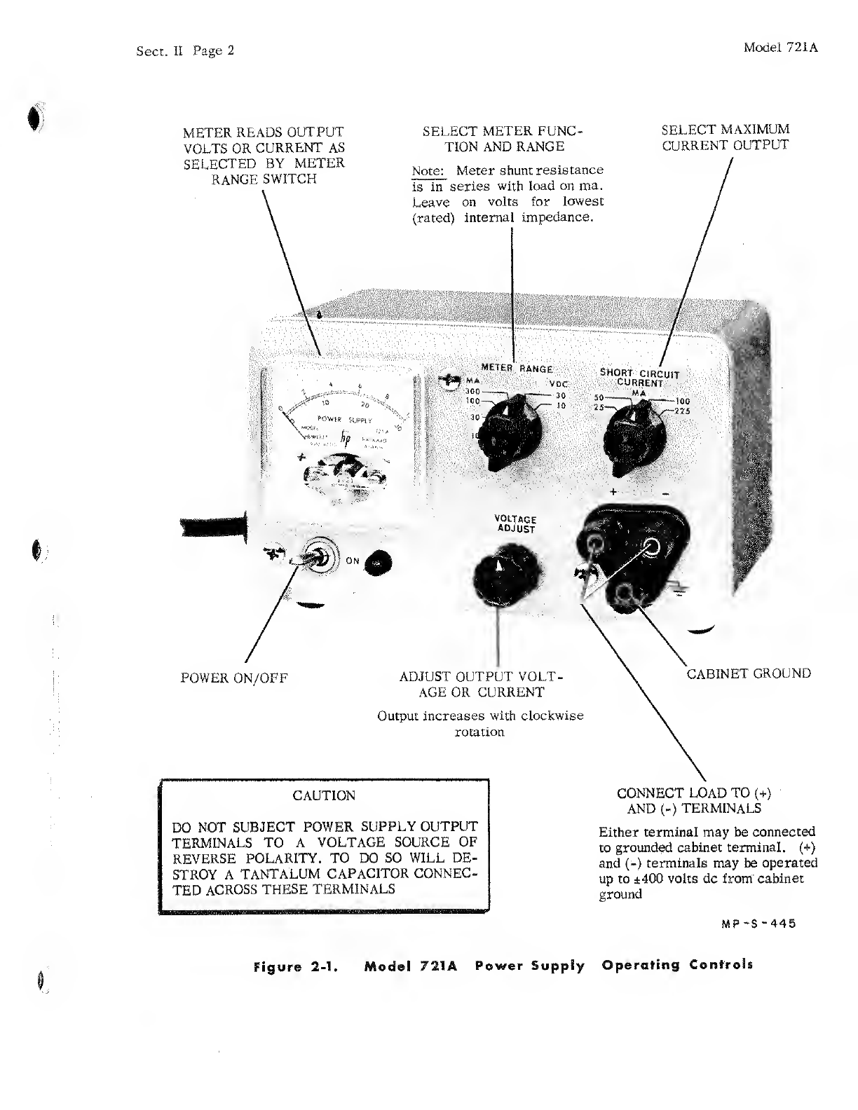
HP 721A Owner's manual

721A
SERIALS
PREFIXED:
024
OPERATING
AND
SERVICING
MANUAL
PRINTED
1/61
00010-2

MODEL
721
A
POWER
SUPPLY
SERIALS
PREFIXED:
024
-
i
«
Copyright
HEWLETT-PACKARD
COMPANY
1959
1501
PAGE
MILL
ROAD,
PALO
ALTO,
CALIFORNIA,
U.S.A
0
printed
1/61
00010-2

Model
721A
SPECIFICATIONS
REGULATED
OUTPUT
VOLTAGE:
0
to
30
volts
dc,
continuously
variable
FULL
LOAD
OUTPUT
CURRENT:
150
ma
over
entire
voltage
range.
LOAD
REGULATION:
With
the
meter
monitoring
voltage,
the
change
in
output
voltage
from
no
load
to
full
load
is
less
than
0.
3%
or
30mv
whichever
is
the
greater.
LINE
REGULATION:
The
change
in
output
voltage
for
a
change
from
nominal
line
voltage
of
±10%
is
less
than
±0.
3%
or
±15
mv
whichever
is
greater.
RIPPLE
AND
NOISE:
Less
than
150
^j.v
rms.
OUTPUT
IMPEDANCE:
Less
than
0.
2
ohm
in
series
with
less
than
30
;ih
with
meter
monitoring
voltage.
METER
RANGES:
Full
scale
indications
of:
10
ma,
30
ma,
100
ma,
300
ma,
10
v
and
30
v.
OVERLOAD
PROTECTION:
Maximum
current
selected
by
switch
in
four
steps,
25
ma,
50
ma.
100
ma,
225
ma.
OUTPUT
TERMINALS:
Three
banana
jacks
spaced
3/4"
apart.
Positive
and
negative
terminals
are
isolated
from
chassis.
A
maximum
of
400
volts
may
be
connected
between
ground
and
either
output
terminal.
POWER:
115/230
volts
±10%,
50
to
60
cps,
16
watts.
WEIGHT:
Net
4
lbs.,
shipping
7
lbs.
DIMENSIONS:
7”
wide,
4-3/8”
high,
5-1/4”
deep.

Model
721A
SECTION
I
SECTION
II
SECTION
III
SECTION
IV
SECTION
V
CONTENTS
GENERAL
INFORMATION
Page
I
-
1
Manual
Content.
!
"
|
1-2
General
Description.
1.-3
Inspection.
1-4
Power
Cable.
r
1
-
5
230
Volt
Operation.
1
"
4
OPERATING
INSTRUCTIONS
2-1
Operating
Controls
..
2-2
Meter
Range
Switch.
2-3
Short
Circuit
Current
Switch
.
2-4
Series
Operation
of
Supplies
.
2-5
Parallel
Operation
of
Supplies
THEORY
OF
OPERATION
.Ill
-
1
3-1
3
-
2
.
...
Ill
-
1
........
Ill
-
1
O
"
D
.Ill
-
1
3-4
.Ill
-
1
3
•“
5
.Ill
-
2
3-0
3
-
7
Frequency
Response
Control.
.Ill
-
2
MAINTENANCE
4-1
Contents.
4-2
General
Maintenance
Information.
4-3
Trouble
Localization.
4-4
Checking
Voltage
Regulation
and
Ripple
.
.
.
4-5
Measuring
AC
Internal
Impedance.
4-6
Meter
Calibration.
4-7
Setting
Maximum
Output
Voltage.
4-8
Calibrating
the
Short
Circuit
Current
Circuit
4-9
Replacing
the
Power
Transistor.
4-10
Replacing
Diodes
CR5,
CR6
and
CR7.
TABLE
OF
REPLACEABLE
PARTS
5-1
Table
of
Replaceable
Parts
IV
-
1
IV
-
1
IV
-
1
IV
-
3
IV
-
3
IV
-
3
IV
-
5
IV
-5
IV
-5
IV
-5
V
-
1

Model
721A
Sect.
I
Page
1
SECTION
I
GENERAL
INFORMATION
1-1
MANUAL
CONTENT
The
material
for
this
instruction
manual
is
written
in
five
sections:
Section
I
contains
material
of
a
general
nature.
Section
II
explains
how
to
operate
the
power
supply.
Section
III
explains
how
the
circuit
operates.
Section
IV
covers
maintenance
and
trouble
shooting
procedures.
Section
V
is
a
table
of
replaceable
parts.
1-2
GENERAL
DESCRIPTION
The
Model
721A
Power
Supply
produces
a
dc
regulated
voltage
adjustable
from
0
to
30
volts.
The
supply
makes
load
circuit
performance
inde¬
pendent
of
external
power
supply
influences.
The
supply
has
very
low
source
impedance
and
ex¬
cellent
regulation
against
change
in
line
and/or
load.
This
supply
is
especially
useful
as
a
source
of
power
for
transistor
circuits.
A
circuit
is
provided
which
electronically
limits
the
maximum
output
cur¬
rent
that
can
be
supplied
to
four
nominal
values
selected
by
a
front
panel
switch.
This
feature
helps
prevent
the
accidental
destruction
of
an
expensive
transistor
should
an
accident
occur
that
would
nor¬
mally
allow
excessive
current
to
flow
through
it.
The
SHORT
CIRCUIT
CURRENT
switch
can
be
set
to
the
value
which
is
closest
above
the
normal
operating
current.
The
supply
will
automatically
limit
the
peak
current
flow
to
this
nominal
value
regardless
of
the
load
resistance.
Built-In
Metering
A
built-in
meter
allows
either
output
voltage
or
current
to
be
monitored
as
selected
by
the
METER
RANGE
switch.
Isolated
Output
The
power
supply
has
both
output
terminals
in¬
sulated
from
chassis
ground.
Either
terminal
may
be
grounded
or
a
number
of
supplies
may
be
con¬
nected
in
series
to
obtain
higher
voltages.
Insula¬
tion
is
such
that
the
supply
may
be
operated
as
high
as
400
volts
off
of
ground.
Parallel
Operation
Parallel
operation
of
two
or
more
supplies
is
pos¬
sible
due
to
the
unique
electronic
current
limiting
switch.
The
supplies
will
each
contribute
only
the
number
of
milliamperes
selected
by
the
SHORT
CIRCUIT
CURRENT
switch.
The
individual
supplies
may
be
loaded
to
approximately
225
ma
with
some
reduction
in
ripple
and
regulation
characteristics.
Reliability
The
Model
72XA
Power
Supply
is
very
compact,
and
has
low
internal
losses,
which
are
made
possible
by
fully
transistorized
circuitry.
The
trouble
free
characteristics
of
transistors
together
with
the
use
of
high
quality
components
throughout,
will
result
in
a
minimum
of
maintenance.
1-3
INSPECTION
When
the
Model
721A
is
received,
inspect
it
for
damage
received
in
transit.
Operate
the
instrument
to
make
certain
that
it
is
functioning
satisfactorily.
If
damage
is
evident,
follow
the
procedures
outlined
in
the
“CLAIM
FOR
DAMAGE
IN
SHIPMENT”
page
of
this
manual.
1-4
POWER
CABLE
The
power
cable
consists
of
three
conductors
and
is
terminated
in
a
three-prong
male
connector
rec¬
ommended
by
the
National
Electrical
Manufac-

Sect,
I
Page
2
00010-2
Model
72iA
turers’
Association.
The
third
contact
is
an
offset
round
pin
added
to
a
standard
two-blade
connector
which
grounds
the
instrument
chassis
when
used
with
an
appropriate
receptacle.
To
use
this
NEMA
connector
in
a
two-contact
receptacle,
a
three-
prong
to
two-prong
adapter
should
be
used.
When
the
adapter
is
used,
the
third
contact
is
terminated
in
a
short
lead
from
the
adapter
which
can
be
con¬
nected
to
the
outlet
mounting
box
in
order
to
ground
the
instrument
cabinet.
1-5
230
VOLT
OPERATION
This
instrument
may
be
easily
converted
from
115
to
230
volt
operation
by
removing
two
jumpers
and
installing
one
jumper.
This
changes
the
dual
115
volt
primary
windings
from
a
parallel
to
a
series
connection.
Refer
to
the
schematic
diagram
and
Figure
4-6
for
details.
The
main
fuse
(FI)
should
be
changed
(see
Table
of
Replaceable
Parts
for
the
correct
type
of
fuse).

Model
721A
Sect.
II
Page
1
SECTION
II
OPERATING
INSTRUCTIONS
2-1
OPERATING
CONTROLS
Figure
2-1
shows
the
function
o'Peach
of
the
controls
and
is
normally
self
explanatory.
There
are
a
few
additional
facts
to
be
considered
which
may
be
im¬
portant
in
some
applications.
2-2
METER
RANGE
SWITCH
This
switch
connects
precision
internal
resistors
into
the
meter
circuit
to
obtain
the
various
voltage
and
current
ranges.
When
measuring
current,
the
meter
shunt
resistor
is
in
series
with
the
output
terminals.
The
meter
shunt
resistance
adds
to
the
source
impedance
of
the
supply
which
is
normally
less
than
0.2
ohm
in
series
with
less
than
30p,h.
The
Table
2-1
lists
the
additional
resistance
for
each
current
range.
Where
minimum
source
im¬
pedance
is
important,
the
METER
RANGE
switch
should
be
left
on
one
of
the
voltage
ranges
except
when
actually
measuring
load
current.
An
accidental
short
circuit
can
damage
the
meter
if
it
is
on
one
of
the
lower
ranges
and
the
SHORT
CIRCUIT
CUR¬
RENT
switch
is
set
to
a
high
value.
Short
time
overloads
of
two
times
full
scale
will
not
damage
the
meter
movement.
2-3
SHORT
CIRCUIT
CURRENT
SWITCH
This
switch
controls
a
circuit
which
adjusts
the
peak
current
output
capability
of
the
supply.
The
cali¬
bration
is
nominal.
The
actual
value
may
be
read
by
shorting
the
supply
and
reading
the
value
on
the
monitor
meter.
The
clipping
action
is
gradual.
Consideration
should
be
given
to
this
characteristic
if
pulse
type
circuits
are
being
supplied.
The
average
current
may
be
within
the
supply
rating
(150
ma)
but
peak
currents
may
be
high
enough
to
cause
the
supply
to
clip.
If
the
switch
is
set
to
a
low
peak
value
this
situation
can
occur
at
low
average
current
levels.
When
pulse
circuits
are
being
supplied,
this
switch
must
be
set
to
a
value
which
is
greater
than
the
peak
cur¬
rent
requirements
of
the
circuit.
The
output
circuit
has
24
jif
capacity
shunting
it,
which
helps
supply
high
current
peaks,.providing
they
are
of
extremely
short
duration.
The
value
of
any
external
capacity
added
will
improve
the
peak
current
capability
but
will
decrease
the
safety
provided
by
the
SHORT
CIRCUIT
CURRENT
switch,
since
the
external
capacity
will
provide
high
surge
currents.
The
surge
currents
may
destroy
external
components
before
the
average
current
increases
sufficiently
inside
the
supply
to
cause
the
limiting
circuits
to
operate.
TABLE
2-1.
ADDITIONAL
INTERNAL
RESISTANCE
Monitor
Meter
Current
Added
Internal
Range
(f.s.)
Resistance
10
ma
10
ohms
30
ma
3.33
ohms
100
ma
1
ohm
300
ma
0.33
ohm
2-4
SERIES
OPERATION
OF
SUPPLIES
When
operating
the
Model
721A
at
a
voltage
more
than
a
few
volts
off
of
ground
be
careful
not
to
accidentally
short
circuit
the
external
circuits
so
the
Model
721A
is
subjected
to
voltages
of
reverse
polarity
or
high
voltages
of
the
same
polarity.
To
do
so
will
instantly
destroy
the
electrolytic
capa¬
citors
in
the
power
supply
and
possibly
the
transis¬
tors.
When
a
number
of
supplies
are
operated
in
series,
be
sure
the
SHORT
CIRCUIT
CURRENT
switch
on
each
supply
is
set
to
the
same
(or
higher)
value
than
maximum
peak
current
desired.

Sect.
II
Page
2
Model
721A
METER
range
SHORT
CIRCUIT
CURRENT
VOLTAGE.
ADJUST.
METER
READS
OUTPUT
VOLTS
OR
CURRENT
AS
SELECTED
BY
METER
RANGE
SWITCH
SELECT
MAXIMUM
CURRENT
OUTPUT
SELECT
METER
FUNC¬
TION
AND
RANGE
Note:
Meter
shunt
resistance
is
in
series
with
load
on
ma.
Leave
on
volts
for
lowest
(rated)
internal
impedance.
POWER
Output
increases
with
clockwise
rotation
CONNECT
LOAD
TO
(+)
AND
(-)
TERMINALS
Either
terminal
may
be
connected
to
grounded
cabinet
terminal.
(+)
and
(-)
terminals
may
be
operated
up
to
±400
volts
dc
from
cabinet
ground
ON/OFF
ADJUST
OUTPUT
VOLT¬
AGE
OR
CURRENT
CABINET
GROUND
CAUTION
DO
NOT
SUBJECT
POWER
SUPPLY
OUTPUT
TERMINALS
TO
A
VOLTAGE
SOURCE
OF
REVERSE
POLARITY.
TO
DO
SO
WILL
DE¬
STROY
A
TANTALUM
CAPACITOR
CONNEC¬
TED
ACROSS
THESE
TERMINALS
MP
-S-445
Figure
2-1
model
721A
Power
Supply
Operating
Controls

Model
7
21A
Sect.n
Page
3
2-5
PARALLEL
OPERATION
QF
SUPPLIES
Two
supplies
may
be
operated
in
parallel
to
supply
loads
in
excess
of
150
ma.
Set
the
SHORT
CIR¬
CUIT
CURRENT
switch
of
the
first
unit
to
maximum
(225
ma).
The
first
supply
becomes
a
225
ma
con¬
stant
current
source.
The
supply
will
furnish
up
to
this
amount
of
current
without
harm,
however
the
regulation
and
ripple
specifications
can
no
longer
be
guaranteed.
Adjust
the
voltage
of"
the
second
supply
to
be
the
same
as
the
first
unit
before
con¬
necting
them
together.
The
second
supply
can
be
made
to
share
load
by
advancing
the
VOLTAGE
ADJUST
control
slightly
clockwise.
The
second
supply
will
furnish
the
regulation
action
up
to
the
limit
of
its
capacity
(150
ma).
The
second
supply
may
be
loaded
beyond
the
150
ma
point
up
to
a
maximum
of
225
ma,
making
a
total
of
450
ma
available.
The
usefulness
of
this
extra
out¬
put
capacity
depends
on
the
performance
required
from
the
supplies.
The
supplies
become
constant
current
sources
when
the
SHORT
CIRCUIT
CUR¬
RENT
limiting
circuit
is
operating.
At
this
point
the
ripple,
source
impedance
and
voltage
regulation
specifications
cannot
apply.
Operation
of
more
than
two
instruments
in
parallel
is
not
recommended
as
the
total
current
capacity
becomes
greater
and
accidental
gross
misadjusted
controls
may
result
in
instability.

THEORY
OF
OPERATION
3-1
GENERAL
CIRCUIT
DESCRIPTION
The
regulation
is
accomplished
in
a
manner
which
is
similar
to
vacuum
tube
type
circuits
.
A
power
type
transistor
in
series
with
the
rectified
output
and
the
load,
acts
like
a
variable
resistor
which
maintains
a
constant
output
voltage
or
current
as
selected
by
the
controls.
The
power
transistor
is
controlled
by
a
two
stage
amplifier
which
amplifies
any
changes
in
the
relative
amplitudes
of
the
output
voltage
and
the
reference
voltage.
The
electronic
short
circuit
current
limiting
switch
is
a
unique
feature
which
is
not
normally
found
in
the
vacuum
tube
counterpart
of
the
supply.
This
circuit
senses
any
increase
in
current
above
a
pre-selected
value
and
in
turn
controls
the
conduction
of
the
power
transistor
to
limit
the
peak
current
to
the
pre-selected
value.
A
detailed
description
of
the
Power
Supply
and
its
operation
follows.
Refer
to
the
schematic
diagram
to
identify
the
various
com¬
ponents.
3-2
MAIN
AND
AUXILIARY
SUPPLY
DESCRIPTION
Transformer
T1
supplies
ac
voltages
to
the
main
and
auxiliary
supplies.
The
main
supply
consists
of
silicon
rectifiers
CR1
and
CR2
and
capacitor
C2.
This
supply
furnishes
about
43
volts
to
the
regulator
circuit.
Silicon
rectifier
CR3,
CR4
and
capacitors
C3,
C4
and
C5
supply
-20
volts,
which
is
required
for
operation
of
the
control
circuits.
Regulator
transistor
Q1
acts
as
a
variable
series
resistance
to
lower
the
voltage
to
the
desired
value,
as
set
by
the
front
panel
VOLTAGE
ADJUST
control
R19.
Q1
conducts
more
current
when
the
base
volt¬
age
goes
more
negative
with
respect
to
the
emitter.
3-3
REFERENCE
VOLTAGE
CR7
is
a
reversed
biased
diode
operating
in
the
break-down
condition.
The
diode
maintains
a
con¬
stant
nominal
7
volts
across
itself,
establishing
a
constant
reference
voltage
between
the
negative
out¬
put
lead
and
the
base
of
Q4.
Q4
is
an
emitter
follower
which
repeats
the
reference
voltage
at
its
emitter
terminal,
less
a
constant
internal
base-
emitter
drop
of
about
0.2
volt.
The
voltage
at
the
emitter
has
a
low
source
impedance,
making
it
insensitive
to
normal
variations
in
current
flow.
The
output
voltage
from
the
(+)
output
bus
is
sampled
by
VOLTAGE
ADJUST
control
R19
which
causes
a
current
flow
through
R20
and
R21.
The
regulator
action
maintains
a
constant
current
through
R19
and
R20.
3-4
REGULATION
CYCLE
DESCRIPTION
Assume
the
output
level
has
been
set
with
R19
and
some
change
has
occurred
which
causes
the
output
voltage
to
rise.
The
voltage
at
the
base
of
Q3
is
that
which
would
appear
across
a
forward
biased
diode
and
is
essentially
constant.
The
electron
current
flow
through
R20
is
constant.
When
the
output
voltage
rises,
part
of
the
normal
electron
flow
into
the
base
of
Q3
is
diverted
through
R19.
The
reduced
base-emitter
electron
current
of
Q3
reduces
the
collector-emitter
electron
current
flow
from
R17
by
a
factor
of
approximately
100.
Since
fewer
electrons
flow
into
the
collector
of
Q3
from
R17
and
thte
-
16
volt
bus,
the
voltage
at
R16
goes
in
a
negative
direction.
This
causes
more
electrons
to
flow
through
R16
into
the
base
of
Q2.
Increased
Q2
base
to
emitter
current
causes
much
higher
collector-emitter
current.
Increased
Q2
collector
current
raises
the
voltage
at
R5
which
reduces
the
base
to
emitter
current
of
Ql.
The
reduced
base-emitter
current
of
Ql
increases
its
collector-emitter
resistance
to
electron
current
flow,
hence
increases
its
collector
to
emitter
volt¬
age
drop.
That
voltage
drop
increases
just
enough
to
compensate
for
the
initial
output
voltage
rise,
maintaining
the
output
voltage
at
a
constant
level.
3-5
SHORT
CIRCUIT
CURRENT
LIMITING
CIRCUIT
The
current
flow
to
the
load
is
sensed
by
a
voltage
drop
across
Rll
ABCD.
Silicon
diode
CR5
is

Sect.
Ill
Page
2
Model
7
21A
forward
biased
approximately
0.4
volt
which
is
not
enough
voltage
to
cause
appreciable
current
flow.
Screwdriver
adjust
control
R8
adjusts
the
value
of
the
forward
bias
slightly
to
calibrate
the
circuit.
The
voltage
at
the
junction
of
R7
andR8
goes
more
negative
as
the
load
current
increases,
which
also
lowers
the
voltage
at
the
base
of
Q2.
Q2
conducts
more
current
which
raises
the
base
voltage
of
Q1
maintaining
the
load
current
at
the
pre-selected
value.
The
SHORT
CIRCUIT
CURRENT
switch
selects
the
value
of
resistance
which
will
give
the
correct
value
of
sensing
voltage
to
cause
the
circuit
to
operate
at
the
load
current
selected.
3-6
OUTPUT
SURGE
PROTECTION
CIRCUIT
Diode
CR6
prevents
a
large
surge
output
when
the
output
VOLTAGE
ADJUST
control
R19
is
set
to
a
low
value
(nearly
full
counterclockwise)
and
the
power
switch
is
turned
off.
This
would
normally
occur
because
the
auxiliary
supply
voltage
decays
faster
than
the
main
supply
due
to
the
large
storage
capacity
of
C2.
When
the
auxiliary
supply
stops,
the
base
voltage
of
Q1
would
not
be
controlled.
Q1
would
then
conduct
very
heavily.
The
resulting
output
surge
could
damage
external
components.
CR6
connects
the
base
of
Q1
to
the
junction
of
R20
and
R21.
This
point
is
normally
about
-0.9
volt.
When
the
supply
is
turned
off,
Q4
stops
conducting
and
this
point
rises
towards
+
40
volts
because
of
the
low
resistance
path
provided
by
R19.
CR6
is
then
forward
biased
and
pulls
the
base
of
Ql
positive
which
cuts
Ql
off,
preventing
any
output
surge.
3-7
FREQUENCY
RESPONSE
CONTROL
CIO
bypasses
R18
for
high
frequencies,
which
raises
gain
of
Q3.
C6
and
R15
provide
negative
feedback
around
Q2
to
improve
the
frequency
response.
C7
bypasses
R19
to
provide
a
constant
maximum
ac
feedback
from
the
dc
output
to
the
control
circuit
amplifier
regardless
of
the
setting
of
R19.
C8
by¬
passes
C9
to
compensate
for
increased
effective
series
resistance
in
C9
at
temperatures
below
0°C.
Cll
provides
low
internal
impedance
at
high
frequencies.
Cl
is
an
rf
bypass
to
eliminate
noise
introduced
by
the
power
line.

Sect.
IV
Page
0
00010-2
Model
721A
SERVICING
ITCHED
CIRCUIT
BOARDS
Excessive
heat
or
pressure
can
lift
the
copper
strip
from
the
board.
Avoid
damage
by
using
a
low
power
soldering
iron
(50
watts
maximum)
and
following
these
instructions.
Copper
that
lifts
off
the
board
should
be
cemented
in
place
with
a
quick
drying
acetate
base
cement
having
good
electrical
insulating
properties.
A
break
in
the
copper
should
be
repaired
by
soldering
a
short
length
of
tinned
copper
wire
across
the
break.
Use
only
high
quality
rosin
core
solder
when
repairing
etched
circuit
boards.
NEVER
USE
PASTE
FLUX.
After
soldering,
clean
off
any
excess
flux
and
coat
the
repaired
area
with
a
high
quality
electrical
varnish
or
lacquer.
When
replacing
components
with
multiple
mounting
pins
such
as
tube
sockets,
electrolytic
capacitors,
and
potentiometers,
it
will
be
necessary
to
lift
each
pin
slightly,
working
around
the
components
several
times
until
it
is
free.
WARNING:
If
the
specific
instructions
outlined
in
the
steps
below
regarding
etched
circuit
boards
without
eyelets
are
not
followed,
extensive
damage
to
the
etched
circuit
board
will
result.
1.
Apply
heat
sparingly
to
lead
of
component
to
be
replaced.
If
lead
of
component
passes
through
an
eyelet
in
the
circuit
board,
apply
heat
on
com¬
ponent
side
of
board.
If
lead
of
component
does
not
pass
through
an
eyelet,
apply
heat
to
con¬
ductor
side
of
board.
3.
Bend
clean
tinned
leads
on
new
part
and
care¬
fully
insert
through
eyelets
or
holes
in
board.
2.
Reheat
solder
in
vacant
eyelet
and
quickly
in¬
sert
a
small
awl
to
clean
inside
of
hole.
If
hole
does
not
have
an
eyelet,
insert
awl
or
a
#57
drill
from
conductor
side
of
board.
4.
Hold
part
against
board
(avoid
overheating)
and
solder
leads.
Apply
heat
to
component
leads
on
correct
side
of
board
as
explained
in
step
1.
In
the
event
that
either
the
circuit
board
has
been
damaged
or
the
conventional
method
is
impractical,
use
method
shown
below.
This
is
especially
applicable
for
circuit
boards
without
eyelets.
3
Clip
lead
as
shown
below.
2.
Bend
protruding
leads
upward.
Bend
lead
of
new
component
around
protruding
lead.
Apply
solder
using
a
pair
of
long
nose
pliers
as
a
heat
sink.
This
procedure
is
used
in
the
field
only
as
an
alternate
means
of
repair.
It
is
not
used
within
the
factory.
Figure
4-1.
Servicing
Etched
Circuit
Boards

Model
721A
Sect.
IV
Page
X
MAINTENANCE
4-1
CONTENTS
This
section
tells
how
to
make
internal
adjustments,
locate
trouble
and
how
to
check
over-all
perform¬
ance.
Paragraphs
4-4
and
4-5
may
be
used
as
a
rapid
performance
check
to
certify
that
the
power
supply
is
operating
within
published
specifications.
These
tests
can
be
made
with
the
instrument
in
its
cabinet.
The
power
supply
has
no
parts
which
have
a
definite
limited
life.
The
instrument
should
operate
indefi¬
nitely
with
no
routine
maintenance,
if
any
parts
are
replaced
you
should
recheck
the
settings
of
the
screwdriver
controls
which
set
the
maximum
output
voltage
(R21)
and
maximum
short
circuit
current
(R8).
Variations
among
parts
may
make
it
neces¬
sary
to
readjust
these
controls
slightly.
Reseal
the
control
with
duco
cement
after
adjustment,
otherwise
the
setting
will
change
with
shock
and
vibration.
A
list
of
possible
troubles
and
the
probable
cause
are
tabulated
in
paragraph
4-3.
In
each
case,
curing
the
trouble
involves
replacing
the
defective
parts,
except
loose
end-clips
on
the
silicon
rectifiers
may
be
repaired
by
slightly
crimping
the
fitting.
Be
careful
when
soldering
on
the
etched
circuit
board.
You
can
cause
damage
by
excessive
heat
or
improper
technique.
Figure
4-1
explains
some
of
the
proper
techniques
to
follow.
Paragraphs
4-4
and
4-5
show
suitable
set-ups
for
checking
power
supply
performance.
The
equipment
and
connections
should
be
followed
carefully
to
avoid
false
results.
This
is
especially
true
when
making
ripple
and
dynamic
ac
impedance
measurements.
Stray
ground
loops
are
easy
to
establish
if
equip¬
ment
grounding
techniques
are
not
carefully
con¬
trolled.
The
relative
position
of
each
instrument
in
the
set-up
should
be
followed.
If
equipment
other
than
that
shown
is
used,
it
should
be
of
equiv¬
alent
performance
and
input
characteristics.
Avoid
long
leads
to
prevent
stray
pick-up.
The
procedure
given
does
not
account
for
power
supply
noise
which
adds
to
the
voltmeter
reading
due
to
internal
impedance.
The
residual
power
supply
noise
represents
a
small
error
at
low
audio
frequencies
when
calculating
the
internal
im¬
pedance.
However,
the
value
obtained
will
be
well
within
rated
performance
even
neglecting*
this
error.
Standard
components
are
used
for
manufacture
of
^instruments
whenever
possible.
Special'com¬
ponents
are
available
directly
from
the
<$
factory.
Perhaps
your
most
convenient
source
for
spare
or
replacement
parts
is
your
local^
Representative
who
maintains
a
parts
stock
for
your
convenience.
When
ordering
parts,
please
specify
instrument
model
and
serial
number
plus
the
component
des¬
cription
and
stock
number
appearing
in
the
Table
of
Replaceable
Parts.
Your
local
($
Representative
also
maintains
com¬
plete
service
facilities
and
specially
trained
per¬
sonnel
to
assist
you
with
any
engineering,
appli¬
cation,
test,
or
repair
problems
you
may
have
with
^instruments.‘
4-3
TROUBLE
LOCALIZATION
Table
4-1
lists
some
possible
troubles
and
their
causes.

Sect.
IV
Page
2
Model
721A
VARIABLE
VOLTAGE
MODEL
400D
TRANSFORMER
READ
NOISE
Figure
4-2
Checking
Voltage
Regulation
and
Ripple

Model
721A
Sect.
IV
Page
3
TABLE
4-1.
TROUBLE
LOCALIZATION
CHART
Trouble
Symptom
Probable
Cause
No
output,
fuse
blows
Shorted
Cl
or
T1
No
output,
fuse
does
not
blow
Shorted
C8
Output
voltage
unstable
Poor
regulation
Wandering
voltage
Defective
reference
diode
CR7.
Poor
regulation
(line
or
load)
Defective
Q1,Q2,Q3,
Q4
or
CR1,
CR2,
CR3,
CR4.
High
noise
or
ripple
on
dc
output
(approxi¬
mately
30
mv
50
to
150
kc)
Open
C6
or
possibly
CIO.
Microphonics
Noisy
R19.
Voltage
control
not
smooth
Defective
R19.
1)
Set
Model
410B
VTVM
to
30
volt
range.
2)
Adjust
Model
7
21A
to
30
volt
output.
3)
Adjust
line
voltage
to
115
volts.
4)
Adjust
Battery-Potentiometer
to
obtain
30
volts.
VTVM
will
then
read
0
volt.
5)
Switch
VTVM
to
1
volt
range.
6)
Adjust
bucking
voltage
so
VTVM
pointer
sits
at
about
1/2
scale.
7)
Switch
from
full
load
to
no
load.
Load
«
200
ohms.
8)
Voltage
will
not
change
more
than
0.3%
(0.09
v)
at
30
volts
output,
which
is
worst
condition.
9)
Repeat
at
20
volts
and
10
volts
if
desired.
(Short
out
one
or
two
66.7
ohm
resistors
to
get
150
ma
rated
load,
depending
on
voltage
selected).
Readjust
bucking
voltage
so
VTVM
is
again
at
mid-scale.
20
v
x
.003
=
60
mv
maximum
change
10
v
x
.003
=
30
mv
maximum
change
At
voltages
less
than
10
volts,
change
from
no
load
to
full
load
will
result
in
less
than
30
mv
change
in
voltage.
10)
Repeat
test
with
line
voltage
at
103
and
127
volts.
11)
Adjust
line
voltage
to
115
volts.
12)
Adjust
output
voltage
to
30
volts
and
load
to
200
ohms
(for
rated
current).
13)
Change
line
voltage
+10%
to
103and
127
volts.
Output
will
change
less
than
.3%
(.09
v).
This
is
worst
condition.
At
outputs
below
5
v
dc,
regulation
is
within
±15
mv.
14)
Measure
ripple
with
Model
400D,
use
1
mv
full
scale
range.
Ripple
+
noise
will
be
less
than
150
/±v
(0.15
mv).
4-5
MEASURING
AC
INTERNAL
IMPEDANCE
The
internal
impedance
of
the
supply
is
affected
by
the
ac
gain
of
the
regulator
circuit.
If
the
supply
has
good
dc
regulation
and
low
ripple
ac
in
the
out¬
put
the
supply
should
also
have
low
ac
impedance.
Figure
4-3
shows
a
suitable
set-up
for
checking
the
internal
ac
impedance
if
desired.
The
set-up
shown
should
be
followed
faithfully
if
meaningful
results
are
to
be
obtained.
The
level
of
signal
to
be
mea¬
sured
is
very
low
and
ground
loops
in
the
system
can
easily
give
very
large
errors.
The
measure¬
ment
is
made
by
driving
a
constant
10
ma
alternat¬
ing
current
through
the
power
supply
and
measuring
the
IZ
drop
across
the
output
terminals.
The
inter¬
nal
impedance
can
be
easily
calculated
by
ohm
,
s
law.
4-6
METER
CALIBRATION
The
meter
mechanical
zero
should
be
accurately
set
before
calibration.
The
correct
way
to
do
this
is
to
rotate
the
adjust
screw
clockwise
until
the
pointer
swings
up
scale
and
then
starts
to
swing
down
scale
toward
zero.
Continue
rotating
the
ad¬
just
screw
clockwise
until
the
pointer
is
exactly
over
zero.
If
you
overshoot,
continue
turning
the
screw
clockwise
until
the
pointer
is
again
approach¬
ing
zero
from
the
up
scale
side.
The
internal
meter
is
calibrated
by
connecting
an
external
standard
milliammeter
across
the
output

Sect.
IV
Page
4
Model
721A
($)
MODEL
200CD
AUDIO
OSCILLATOR
5
CPS-600KC
ADJUST
OUTPUT
TO
MAIN¬
TAIN
10
VOLTS
DROP
(10
MA)
ACROSS
1000
OHM
RESISTOR.
1*1.
E
*>
CAUTtOH:
I
AC
.010
Observe
polarity
to
prevent
blocking
capacitor
failure.
Figure
4-3
Measuring
AC
Infernal
Impedance

Model
721A
Sect.
IV
Page
5
terminals
in
series
with
approximately
1,000
ohms.
The
output
VOLTAGE
ADJUST
control
should
be
advanced
until
the
standard
meter
indicates
10
ma.
The
internal
meter
should
be
switched
to
the
10
ma
range.
Adjust
R25
until
the
internal
meter
reads
the
same
as
the
external
meter.
All
other
current
and
voltage
calibrations
will
then
be
determined
by
the
precision
current
and
voltage
multiplier
resis¬
tors
associated
with
the
METER
RANGE
switch.
4-7
SETTING
MAXIMUM
OUTPUT
VOLTAGE
The
maximum
output
voltage
should
be
set
to
be
31
volts.
1)
Turn
the
VOLTAGE
ADJUST
control
full
clock¬
wise.
2)
Measure
the
output
voltage
with
either
internal
voltmeter
or
an
external
standard
voltmeter.
3)
Adjust
R21
to
obtain
31
volts.
4)
Reseal
the
control
with
duco
cement.
4-8
CALIBRATING
THE
SHORT
CIRCUIT
CURRENT
CIRCUIT
1)
Rotate
the
SHORT
CIRCUIT
CURRENT
switch
to
225
ma.
2)
Short
circuit
the
output
terminals.
3)
Rotate
the
VOLT
AGE
ADJUST
control
full
clock¬
wise.
4)
A
djust
R8
to
obtain
230
ma.
NOTE
This
adjustment
provides
the
best
over-all
cali¬
bration
of
this
circuit
on
all
ranges.
The
circuit
is
slightly
temperature
sensitive.
With
the
instru¬
ment
in
its
cabinet
and
hot,
the
maximum
current
available
will
be
approximately
225
ma.
5)
R
eseal
the
control
with
duco
cement.
4-9
REPLACING
THE
POWER
TRANSISTOR
If
you
replace
the
power
transistor
(Ql)
be
careful
to
note
how
the
nylon
bushings
are
installed
in
the
transistor
mounting
holes.
They
must
be
reinstalled
properly
since
the
case
of
the
transistor
is
not
at
chassis
potential.
You
should
also
check
that
there
are
no
burrs
on
the
transistor
case
which
can
cut
through
the
anodized
surface
of
the
mounting
plate.
The
anodized
surface
acts
as
a
good
electrical
in¬
sulator
while
allowing
good
heat
transfer
from
the
transistor.
If
this
surface
is
damaged
the
maximum
voltage
at
which
the
power
supply
can
be
operated
off
of
ground
potential
may
be
reduced.
4-10
REPLACING
DIODES
CR5,
CR6
AND
CR7
The
diodes
CR5,
CR6
and
GR7
are
manufactured
by
They
have
carefully
controlled
character¬
istics
which
result
in
a
superior
performing
instru¬
ment.
Should
replacement
be
necessary
we
rec¬
ommend
that
you
use
similar
diodes.
You
may
obtain
these
from
your
local
(^Representative
or
by
ordering
directly
from
the
factory.
The
cathode
end
of
the
diode
is
marked
with
a
spot
of
red
paint.

Sect.
IV
Page
6
Model
7
21A
O
H
h-
PHW3
CC
Dd
OHil-
X
UJ
O
3
(/)</)<
O
no'r
O
C
=3
H
X
°
U_
CVl
O

■
i^/SgK
mrl
Model
721A
R
11
SHORT
Cl
RCUIT-
CURRENT
SHUNT
R
24
METER
CURRENT
SHUNT
JUMPER
115V
ONLY
EMITTER
1/4
AMP
SLOW
BLOW
(115V)
1/8
AMP
SLOW
BLOW
(230V)
Rear
Interna!
View

Sect.
IV
Page
8
00010-2
Model
721A
Table of contents
Other HP Power Supply manuals