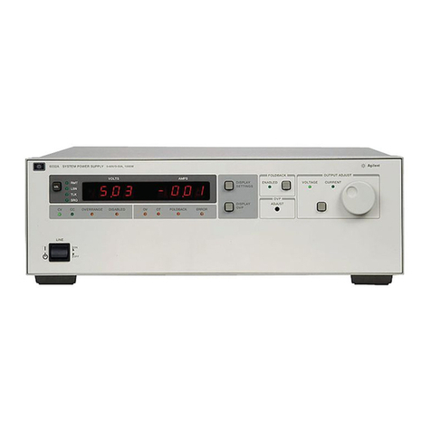
HP HVB Series User manual

DC
POWER SUPPLY
HVB
SERIES,
MODEL
6516A
SERIAL NUMBER PREFIX
7C
Printed: October, 1967
@
Stock Number: 06516-90001

TABLE OF CONTENTS
section Page No.
I GENERAL INFORMATION.
...
.
..
..
....
.l-1
1-
1 Description 1-1
1-4 Overload Protection 1-1
1-7 Cooling 1-1
1-9 Output Terminals 1-1
1-1
1
Specifications 1-1
1-13 Options 1-1
1-15 Accessories 1-1
1-17 Instrument Identification 1-2
1
-
20 Ordering Additional Manuals 1-2
I I INSTALLATION
..
.
.....
...
.
.
.
.
.
2- 1 Initial Inspection
2-3 Mechanical Check
2-5 Electrical Check
2-7 Installation Data
2-9 Location
2-1 1 Rack Mounting
2- 15 Input Power Requirements
2-17 Power Cable
2-20 Repackaging for Shipment
III OPERATING INSTRUCTIONS.
.
.
..
.
.
.
..
.3-1
3-1 Turn-on Check Out Procedure 3-1
3-3 Operation 3-1
3-5 Current Limit Provisions 3-1
3-7 Operation of Supply Beyond
Rated Output 3-1
3-9 Load Connection 3-1
3-13 Output Capacitance 3-2
3- 15 Reverse Current Loading 3-2
3- 17 Reverse Voltage Loading 3-2
IV PRINCIPLES OF OPERATION
...
.
..
....
.4-1
4-1 Overall Block Diagram
Discussion 4-2
4-8 Simplified Schematic Discussion 4-3
4-12 Detailed Circuit Analysis 4-4
4-13 Series Regulator 4-4
4-15 Constant Voltage Input Circuit 4-4
4-20 Driver Amplifier 4-4
4-22 Current Limit Circuit 4-4
Section Page No.
I
V
PRINCIPLES OF OPERATION (Continued)
4-24 High Voltage Control and
Doubler Circuits 4-4
4-28 Protection Circuit 4-5
4-30 Reference Regulator 4-5
V
MAINTENANCE.
..
.
.
..
.
....
.
......
.
.
.5-1
5-1 Introduction 5-1
5-3 High Voltage Precautions 5-1
5-6 Measurement Techniques 5-1
5-9 Test Equipment Required. 5-1
5-1 1 Performance Test 5-4
5-14 Rated Output, Meter, and Output
Controls Accuracy 5-4
5-1 7 Load Regulation 5-4
5- 19 Line Regulation 5-5
5-21 Ripple and Noise 5-5
5-3 5 Transient Recovery Time 5-7
5-39 Output Impedance 5-8
5-42 Temperature Coefficient 5-9
5-46 Output Stability 5-9
5-49 Current Limit 5-10
5-51 Troubleshooting 5-10
5-55 Overall Troubleshooting
Procedure 5-10
5-59 Repair and Replacement 5-15
5-61 Adjustment and Calibration 5-17
5-62 Meter Zero 5-17
5-64 Meter Accuracy Adjustment 5-17
5-66 Output Voltage (Programming
Current) Adjustment 5-17
5-68 Output Current Limit Adjustment 5-17
5-70 Overvoltage Protection 5-17
V
I
REPLACEABLE PARTS
.
..
.
..
...
..
.....
.6-1
6- 1 Introduction 6-1
6-4 Ordering Information 6-1
Reference Designators
Abbreviations
Manufacturers
6-8 Code List of Manufacturers 6-2
Parts List Table 6-5

EUROPE, NORTH AFRICA AND MIDDLE EAST
NORWAY
HsrrMt-Pacurd
US
OsladLn I8
PO Box34
N-13450SleM
TeI 1021 1711 W
T&
16621 hmxn
ITALY
HsrrMt-PackardIWaS
P
A.
Vil
Amango Vow2
caw
pcruld3645
1-20124M1l.m
TOI:
[m 6251 110fins)
w:
hEwpAcK1~
~h
T*a: 32016
HsrrMt.hckard
Illull
S.P.A.
mPsXuD9
1.351w P.*.
Td 10491 66 48 88
Th41612 HWCh
UNITED KINGDOM
HtrMt.Parkard Lld
~&?AZ2,0wo~nphlm
bkr
RGII MA
Tel 10734) 78 47 74
?E~"rpad-=-
Herlm.Pacbrd Lld
Tn1q.l HWw
NawalaAd
Altrlncham
CherhlreWAl4 INU
Td (0611 926 6422
Tdu
668068
Hewleu Packard Lld
L
gun
cwn
&ward RIM
Dudley Road
Hm1w01.nWest Mldlandr 862 IS0
Tll' 1021 550 5311
T*.: 33b105
WUND
0b.m
lntomlqTerhdanq
Mm-Rckard
UI
Slnli2.6P
W-950W.nzawa
Td:
33
25 8M967 43
T& 61 24 53 hem
d
SWEDEN
H&n.Packard Sarw
I
:;%;"B22
2"
Tel lOBl 730 05 M
Tder 10721
Cable MEASUREMENIS
.
.
UNIPAN
Bbro
WIlWl
1sdlnKInei
01.447 warslaw1
YI
IY.mlshm 6
H&n ~ackard
IW~W
S p A
Vn G Armdht 10
I-WI43Rw
Tel :06) 54 69 61
Telex 61514
Cabk
HEWPACKIT
Rwru
m-hckardIukanaS
P
A
ccm
GlovannaLam
U
1-10133Torlno
Tel1011) 66224Y6593011
MecmUCalcubmnonly
Ht.lsll.hcWd IUUmS PA
%;2%3l:I
Tell095137 05 M
PORTUGAL
Ta(ann-Emvol 16- de
E~~mcntaRUI
Rcdiiy
da
U(culom
FmwaS.a.r.1.103
P.O.
Box
531
P-U.bm 1
bl:
119 68 W 72
w:
LECTRI
LUm
T&x 125811
H~rMt.PatkaldLld.
wee+
Hwse
753. LMdDn Road
GB-Thantm Hulh
SUtr CRl ML
Tel: $1)
684
0103,6
Tdrr' 946625
P.O. Box 307
CH-85% SshHmnZvrWl
PI:
Th:(01)539337305240hfp
dl
PMl.
"PAP.
r.
end
EleRrmr Im:
~uriBuha-Umd
Ebn
UyrSlrwl
P 0
80.
5711
O.MCU.
JORDAN
Mouashlr
COullns
Co
PO Bor1381
iG:
T~X:
Ufii711215 tnw
w:
ELECTROBOR DAMASCUS
Me&dPmona Wcucrlor
o*
%"nh
.4
co
Pllm
kmd
8P
2JOB
Damamcum
TeI 16567-19 697-14 266
Tdo: 11x4S*TACOSY
WeSAWAH OAMLSWS
Su(mman
HIW El MINI
P 0
Box
2528
Mamwn Blur SIR(1
SbY)
Om~mcusTd1146
63
Tdez 11270
CWa HlUL OAMASCUS
NNIYA
Tunme31 AwweEl~lrdez~Wlntl
RUMANIA
Herlm-Pachard
rwmmnUM
MnWwsw16
BYSUmu
TeI 15 W 2313 88 65
T& IOU0
KUWAIT
w~hak&ya Twna
6
P 0%3s*
Kunll
Tell2491ONl 1728
Th241A
UW
WSM#ld
MOROCCO
Odb.."
NRKEY
TEKNIM
h
ny
Ltd
RIP
%h
P%I
'
Caddl1
NO.
7
hakwle.Anhmn
TeI' 27W
Tskx 42155 TKNM
TR
%%d
8- Roudanl
WuM.nu
Tll: 25 16 71V15 W
89
T& 21n9
CWs
GEREP US*
Modem
Ummniz
EmMrhmew IBnndIl
P 0
Box
193
NXh0b.f
Tel 44678-44813
Mr.
67014 OlESTA
C&
ELECTA AL-KHOQAR
Mdul
M(y
E MA.
Muhen&skk KWl%lull
MdhaEldmSokak 4116
YJLIrl Caddll
ADhmR
Tel 17 56 22
CaMa EMLTRIDUlnMla
Wls
Jau
3
E-M.M 3
nl
11 tsa 26
w
[to ins)
Te. '23515
hl.
FOROTHERAREAS
NOT USTED CONTACT
Hmim.Packard S
A
7
rue
du B0Cs.d~Lan
~---
malvltalonly
vW
Ormnk
MliMuddv
Cad
1616
MYAnhm,.
Tel 250109-178026
Th42576 OZEK TR
CaMa OZYUREKANURI
NETHERLANOS
HaM1.PabUd
fmW
N V
Van Hwn
Goldhamaan
121
PO Box667
NL-Amst-n 1134
Td IOMI 47 20 21
uw
PILOBEN Amstadam
PO Box
CH.1217 Meyno 2 Gonsvm
SwlQ~nlnd
Tdcable(022HLwPAcKsA62 70 W Gln~l
OREGON
178~
sw
~wer
her
brr,
Amad
TuahUn 97062
Td. (5m) 6203350
ALABAMA
9606
Aero Om8
P 0 Box 23333
5."
Dlqo92123
181 (714) 27s32m
7mn.n.
Tsl 1213) 705-3244
COLORADO
5690
OTC
Pam
En(lln*md 1110
Tel 1303) 771-3455
CONNECTICUT
12
LWI
Orwe
Nnr
hrm
06525
Tel (203 309.6551
Tm
71b465.2029
PO
b14207
8290 WnttcsburpOr
H~nlsYIlh3Y102
Tel 12051881.4591
6933 E RoetMh Wd
Blrrnl hmm 35206
RI
(31836.220312
HAWAII
21175
So
Kt Strefl
HDnolulu %6
To1
(MXI)
%5-4455
ILUNMS
5201 T&sw Or
ROlll Yudar86MOB
Trl (82 255-9800
TWX
91bW.22~
INDIANA
7301 NWh ShadlndAW
IOWA
2415 HMRoad
la*.
Cky
52240
184. 1319) 32d.9466
KENNCKY
Ma1OW
3901 Ahinsan01
%lta 407 A1Umon
Wm
Loul.v(ll. 4118
Tal (WZ) 456.1573
LOUISIANA
P 0 801 1449
3229.59 WilYIml Boulsrard
Kmnm
70063
Tel ISMI 443.6201
PENNSYLVANIA
111
ZPtl
Orlt
Pl-nph 15236
lev
14121 71244W
MINNESOTA
24W N PrwAn
St. P.ulslt3
Tel 1612) 6MO7W UTAH
2160 SWlh 3270 WeslSlrml
%n
Laha Clty 84119
Tel (Boll 972.4711
ARIZONA
23% E Ma
Wl
S1
Ph-1.
&
Tal IW21244.1561 WERTORlCO
H1YM1.Packard 1nltr.Ameriur
Pueflo
ASO
nnncn OMW
Cdh
272
~01.C.rdlm2m.w08924
cwwv
~ub
Td. IMP)) 762-7255
Tda: 345 G514
VIROINA
P.0 Box 12776
NO
7 Koprr Emanter
SU,te 212
Naldk23502
Tal. (MU) 461-402516
P 0 Box 9669
2914 Hvnpr,
%rows
Rod
Rlshmond 23228
Tll. (MU) 205-3431
'ARKANSAS
Maul
Lmca
OM
P 0 Box 5646
~ndySutmn
LlnhRock 72215
Td (5011376-1844
FLORIDA
P 0 80.24210
2727
N
w
62nd Salt
Fl. Laud.rd.k 33309
Tel
(305)
973.26W
4428
Emstson
YmI
Uml I03J.sk.onvlll. 32207
Tel 1904) 725-hlU
P 0
Boa
13910
6177 Lala ElnorOr
Orlenda 32009
Tel 1305) 854.29W
P 0 Box 12626
%E15hk"RBh
P.""coI. 52575
Tel 1904) 476-0422
.
.
.
..
-
-.
114GmlWhllWlY
Y.
LOYIS63141
Td: 1314) 171anxl NORTH CARWNA
5605
RomnaWay
Gmnsbwo27405
Tel: 1919I152.1MD SOUTH CARWNA
P 0 8016442
6941.0
N.
TrsnMlm Road
CdumM
29260
Tel: [M3(LI) 782-6493
TENNESSEE
8914
K'
tmRks
Knolvx 37922
Tel: (6151 521.0522
3027 vanpwrd Or
Dlmeor's
m
IS
AW
MI31
Td (GI 146-1370
'NamhYIIhMad
Samf€s
Tel 1615) 244.~3
TEXAS
4171 NOM MPI
SullaElPasoCllO79902
TeI (915) 533-3555
P 0 Box 1270
201
E
Anprho Rd
Rkh.,d.w, 75400
To1 (214) 231.6101
NEBRASKA
Funo,"#old
SulW ID
OMh.
66106
14 141) 392-osts
. .
OHIO
MadkVCwbrOW
33
E.*W
Rd
Clnelma1145426
Tel. (513) 671-7100
IW
spnpw Rd
Clmvmlmnd 44130
TeI (216 243.73W
TWX
01b423-9430
UO
Prwlers
Rd
D.,ion 45449
101 (513) 15P8202
1M1KlngsmYI Parkway
Columbus 43229
T& (614) 4MlM1
OKLAHOMA
PO Box3M08
6301 N MeMan Awnurn
OLImhommCI 73112
PI
1405) 721-0rPO
4110 S 1KUh E Awnue
GnW
W
Tvlu
74145
CALIFORNIA
I430 EYI OR ~lhwrdAM
Fullwtm9281
Tcl !I141 8701WO
3939 Lanbrshlm Boutward
NathHd wmd91604
Tel 1213 877-1282
TWX
91b499.2671
WASHINGTON
BM~eldOnlcr Pk.
12m-lllhAve. S
E
BeIIwuo98004
181:TWX:(2061454.3911OI0443.2446
'WEST VIRGINIA
MeMuUAnrlvlKalOoh
ChmrlalonTcl [MI)345-1640YWWet ROIICRN Wd
P 0 Box 92105
World Way PsulCentu
. .
NEW JERSEV
W 120 Cmlury Rd
Paramus 07652
bl
(201 265.5m.l
TWX
7lb9904%1
. .
MARYLAND
6707 Whltslme Road
8.Rlmon 21207
RI
1301 944 YW
rwx
~~~~~9157
2ChokaChn Road
Roskvlll.
&
Tel (301 US6370
Tm
71b-828-96~
WISCONSIN
9w4West bncdn Ave
WellTd: (414)A111. 541-055053227
GEORGIA
P 0 Box 105005
450 InlerrUts Norm Plrllly
Al1.n~ 30348
181 (4M) 955-1500
TWX
8lC-766-41190
FOR
u.S. AREAS NOT LISTED:
Cmlacl Iht
rwd
OIkO
nurest
vou Auanla. GeolOla
Msdlul
Lmp
Only
;:Y4%7Ea
i-&hHh&wd.
c~ormi
RwMlc. Maryland RdkW *UdO*s.
IbmisThur m&le
.ddmcs are hsted
aPve
;:;%;%-6165
646 W
Nonh
Mark81Wd
Smsnmnlo95634
Td 1916) 9297222
MASSACHUSETTS
32 Ham11Ave
P 0 'Bo1'2103
1172 N Dams orbe
WnnnRoblns 31098
Tel (912) 9224448

m
HIGH
VOLTAGE CONTROL CIRCUIT WAVEFORMS
I
NORMAL WAVEFORMS
I
TP(II) TO
(+)
Il5VAC INPUT TP(II) TO
(+)
115VAC INPUT
2OV/CM TP(II) TO
(+)
II5VAC INPUT
3000V/6MA OUTPUT POV/CM
10MS/CM 1500V/6MA OUTPUT 2OV/CM OVIOMA OUTPUT
IOMS/CM IOMS/CM
Ov-
r
*
I
oov-
140V-
h
TP(36) TO
(f)
115VAC INPUT TP(36) TO
(+I
II5VAC INPUT TP(36) TO
(+I
2OV/CM I15VAC INPUT
3000V/6MA OUTPUT LOV/CM 1500V/6MA OUTPUT 2OV/CM
IOMS/CM OV/OMA OUTPUT
IOMS/CM IOMS/CM
TP(36) TO
(+)
lO5VAC INPUT
5V/CM OV/OMA OUTPUT
IOMS/CM
r-
--
\Tk
FIRING
TP(36) TO(+) IO5VAC INPUT
5V/CM 500V/2MA OUTPUT
IOMS/CM
TYPICAL TROUBLES
TP(II) TO
(+I
I15VAC INPUT TP(36) TO
(+)
I15VAC INPUT
2OV/CM 3000V/6MA OUTPUT POV/CM 3000V/6 MA OUTPUT
IOMS/CM IOMS/CM
WAVEFORM INDICATES MISADJUSTMENT OF PROTECTION WAVEFORM INDICATES ONE SCR (CR7 OR CR40)
CIRCUIT. NOTE THAT NEGATIVE PEAK IS TOUCHING NOT FIRING. NOTE POSITIVE PEAKS TOUCH OV
OV BASE LINE. BASE LINE
h
NOTE
-
ALL WAVEFORMS ARE DC COUPLED.

LIST OF TABLES
Table
Page
No.
1-
1 Specifications.
.
........
..
..
.
..
.
...
.
......
.
1-3
5-1 Test Equipment..
.
...
.
..
.
.
..
..
.
.
..
.
.
.
.
.
.
.
.
.
5-3
5-2 Bias. Reference, and Rectifier Voltages.
.
..
.
.
.
5-10
5-3 Low Output Voltage Troubleshooting..
...
.
.
.
..
5-12
5-4 High Output Voltage Troubleshooting
.
.
.
..
.
.
..
5-14
LIST OF ILLUSTRATIONS
Figure Page No.
1-1 DC Power Supply
i
v
2-1 Rack mounting, Two Units 2-1
2-2 Rack Mounting, One Unit 2-2
3-1 Front Panel Controls and Indicators 3-1
4-1 Overall Block Diagram 4-
1
4-2 Simplified Schematic Diagram 4-3
5-1 High Voltage and Troubleshooting
Location Diagram 5-2
5-2 Differential Voltmeter Substitute,
Test Setup 5-4
Figure Page No.
5-3 Line and Load Regulation.
Test Setup 5-4
5-4 Ripple and Noise, Test Setup 5-5
5-5 High Voltage Protection Network 5-6
5-6 Noise Spikes, Test Setup 5-7
5-7 Transient Recovery Time, Test Setup 5-8
5-8 Transient Recovery Time Waveforms 5-8
5-9 Output Impedance, Test Setup 5-8
5- 10 Servicing Printed Wiring Boards 5-16

t
ARR
SON
OWER
SUPPLY
W
.
PA
-
LINE
P
5H
O.I/OrF
Figure 1-1.
DC
Power Supply, Model 6516A

SECTION I
GENERAL INFORMATION
1-1
DESCRIPTION 1-9 OUTPUT TERMINALS
1-2 This instrument (Figure
1-1)
is
an all semi-
conductor high voltage supply suitable for either
bench or relay rack operation. It
is
a compact,
well-regulated. Constant ~oltage/CurrentLimited
supply that will furnish 3, 000 volts at 6 milliamps
or can be adjusted throughout the output voltage
range. It
is
designed for applications requiring
extreme stability, regulation, and insensitivity to
ambient temperature variations.
1-3 This supply utilizes a series regulated
"piggy-back" circuit technique that consists of
placing a well-regulated low voltage power supply
in series with a
less
well-regulated supply having
a greater voltage capability. The well-regulated
"piggy-back" supply continuously compensates for
any ripple, load regulation, or line regulation de-
ficiencies of the main power source and adjusts
the voltage across its series regulator sothat the
total output voltage remains constant despite dis-
turbances in the main voltage source.
1
-4 OVERLOAD PROTECTION
1-5 The voltage thumbwheel switches select the
constant voltage level; an internal potentiometer
selects the current limit level. The supply will
automatically crossover from constant voltage to
current limit operation and vice versa if the output
current or voltage exceeds these preset levels.
Detailed characteristics of the output current lim-
iting are given in Paragraph 3-5.
1-6 The power supply
is
protected from reverse
voltage (positive voltage applied to negative ter-
minal) by an internal protection diode that shunts
current across the output terminals when this con-
dition exists, clamping the reverse voltage. Pro-
tection from reverse current (current forced into
the power supply in the direction opposite to the
output current) must be provided by preloading the
power supply (Paragraph 3-15). The power supply
cannot accept reverse current without damage.
1-7 COOLING
1-8 Convection cooling
is
used; no fan
is
re-
quired. The power supply has no moving parts
except for the meter movement.
1-10 Output power
is
available via two UG-931/U
connectors mounted on the front panel of the sup-
ply. Mating connectors (UG-932/U) are supplied
with the unit. The output terminals are isolated
from the chassis and either the positive or the neg-
ative terminal may be connected to the chassis by
shorting the center pin to the case of the applica-
ble ~G-931/~connector, or by grounding a wire
from the connector to the chassis. The power sup-
ply
is
insulated to permit operation up to 1,000
volts dc off ground,
i.
e.
the maximum potential
between either output terminal and ground shall not
exceed 4KVdc.
1-11
SPECIFICATIONS
1-12 Detailed specifications for the power supply
are given in Table
1-1.
1-13 OPTIONS
1-14 Options are factory modifications of a stand-
ard instrument that are requested by the customer.
The following options are available for the instru-
ment covered by this manual. Where necessary,
detailed option information (operation, alignment,
etc.
)
is
included throughout the manual.
Option No. Description
50Hz Input Modification. Factory
modification includes the substitution
of 60Hz with 50Hz magnetic compo-
nent as indicated at the end of the
parts list in Section VI. In addition,
the overvoltage protection adjustment
is
rechecked, refer to Section
V.
230Vac &lo%. Sinqle-Phase Input.
Factory modification includes the in-
stallation of a 230 volt input trans-
former to replace the standard 115volt
transformers as indicated at the rear
of the parts list in Section VI.
1-15 ACCESSORIES
1-16 The accessories listed in the following chart
may be ordered with the power supply or separately

from your local
@
sales office. (Refer to list at
rear of manual for addresses.
)
Additional informa-
tion on accessories
is
given in Section 11.
@
Part No, Description
14515A Rack Kit for Mounting one 5a" H
supply in a standard 19" EIA rack.
(Refer to Section
I1
for details.
)
14525A Rack Kit for mounting two 5;"
H
supplies in a standard 19" EIA rack.
(Refer to Section I1 for details.
)
INSTRUMENT IDENTIFICATION
1-1
8
Hewlett-Packard power supplies are identi-
fied by a three-part serial number tag. The first
part
is
the power supply model number. The sec-
ond part
is
the serial number prefix, which consists
of a number-letter combination that denotes the
date of a significant design change. The number
designates the year, and the letter A through
L
designates the month, January through December,
respectively. The third part
is
the power supply
serial number; a different sequential number
is
as-
signed to each power supply.
1-19 If the serial number prefix on your power
supply does not agree with the prefix on the title
page of this manual, use the change page that
is
included to update the manual to the proper serial
number. Where applicable, backdating information
is
given in an appendix at the rear of the manual.
1-20 ORDERING ADDITIONAL MANUALS
1-21 One manual
is
shipped with each power sup-
ply. Additional manuals may be purchased from
your local
@
sales office (see list at rear of this
manual for addresses). Specify the model number,
serial number prefix, and
@
stock number provided
on the title page.

Table 1-1. Specifications
OUTPUT: voltage
is
defined as the mean between the no
0-3000Vdc, 0-6 milliamperes. load and full load voltage.
INPUT: OVERLOAD PROTECTION:
115VacrtlO%, single phase, 57-63Hz, lA, 40W. An all electronic, continuously acting current
limit protects the power supply for all overloads
LOAD REGULATION: regardless of how long imposed, including a di-
Less than 0.01% or 16mV (whichever
is
greater) rect short circuit across the output terminals.
output voltage change for a full load to no load
change in output current. CONTROLS:
An in-line 4-digit (thumbwheel) voltage program-
LINE REGULATION: mer permits control of the output voltage; resolu-
Less than 0.01% or 16mV (whichever
is
greater) tion
is
1V.
output voltage change for a 10%change in the
nominal line voltage. METER:
The front panel meter is a 0-3500V voltmeter.
RIPPLE AND NOISE:
Less than 2mVrms, 5mV p-p. OUTPUT TERMINALS:
The dc output of the supply
is
floating; thus,
TEMPERATURE RANGES: the supply can be used as either a positive or
Operating:
0
to 55OC. Storage: -20 to +85OC. negative source. Terminals for tOUT, -OUT,
and GND are provided on the front of the supply.
TEMPERATURE COEFFICIENT:
Less than 0. 02% t2mV output voltage change COOLING:
per OC after 30 minute warm-up. Convection cooling
is
employed. The supply
has no moving parts.
STABILITY:
Less than 0. 05% t5mV total drift for 8 hours SIZE:
after 30 minute warm-up and with 30C ambient 8+" W
x
5;" H
x
16"
D.
Two of the units can be
variation. mounted side by side in a standard 19" relay rack.
OUTPUT IMPEDANCE:
Less than 32 ohms from dc to 30Hz. WEIGHT:
17 lbs. net, 20 lbs. shipping.
Less than 8 ohms from 30Hz to 100kHz.
Less than 2 ohms from lOOkHz to 1MHz. FINISH:
TRANSIENT RECOVERY TIME: Light gray front panel with dark gray case.
Less than 100pseconds
is
required for output
voltage to recover to within 0.01% or 16mV
of
the POWER CORD:
nominal output voltage following a full load A 3-wire 5-foot power cord
is
provided with each
change in output current. The nominal output unit.

SECTION I1
INSTALLATION
2-1 INITIAL INSPECTION
2-2 Before shipment, this instrument was in-
spected and found to be free of mechanical and
electrical defects. As soon as the instrument
is
unpacked, iuspect for any damage that may have
occurred in transit. Save all packing materials
until the inspection
is
completed. If damage
is
found, proceed as described in the Claim for
Damage in Shipment section of the warranty page
at the rear of this manual.
2-3 MECHANICAL CHECK
2-4 This check should confirm thqt there are no
broken knobs or connectors, that the cabinet and
panel surfaces are free of dents and scratches,
and that the meter
is
not scratched or cracked.
2-5 ELECTRICAL CHECK
2-6 The instrument should be checked against
its electrical specifications. Section
V
includes
an "in-cabinet" performance check to verify proper
instrument operation.
2-7 INSTALLATION DATA
2-8 The instrument
is
shipped ready for bench
operation. It
is
necessary only to connect the in-
strument to a source of power and it
is
ready for
operation.
2-9 LOCATION
2-10 This instrument
is
air cooled. Sufficient
space should be allotted sothat a free flow of
cooling air can reach the sides and rear of the in-
strument when it
is
in operation. It should be used
in an area where the ambient temperature does not
exceed 550C.
2-11 RACK MOUNTING
2-12 This instrument may be rack mounted in a
standard
19
inch rack panel either alongside a
similar unit or by itself. Figures 2-1 and 2-2
show how both types of installations are accom-
plished.
Figure 2-1. Rack Mounting, Two Units
2-1

2-13 To mount two units side-by-side, proceed
asfollows:
a. Remove the four screws from the front
panels of both units.
b. Slide rack mounting ears between the
front panel and case of each unit.
c. Slide combining strip between the front
panels and cases of the two units.
d. After fastening rear portions of units to-
gether using the bolt, nut, and spacer, replace
panel screws.
2-14 To mount a single unit in the rack panel,
proceed as follows:
a. Bolt rack mounting ears, combining
strips, and angle brackets to each side of center
spacing panels. Angle brackets are placed be-
hind combining strips as shown in Figure 2-2.
b. Remove four screws from front panel of
unit. c. Slide combining strips between front
panel and case of unit.
d. Bolt angle brackets to front sides of case
and replace front panel screws.
2-15 INPUT POWER REQUIREMENTS
2-16 This power supply
is
operated from a nominal
115 volt 60 Hz powei source. The input power re-
quired when operated from a 115 volt 60 Hz power
source at full load is:
Model 6110A 60 Watts
Model 6516A 40 Watts
2-17 POWER CABLE
2-18 To protect operating personnel, the National
Electrical Manufacturers Association (NEMA) rec-
ommends that the instrument panel and cabinet be
grounded. This instrument
is
equipped with a
three conductor power cable. The third conductor
is the ground conductor and when the cable
is
plugged into an appropriate receptacle, the instru-
ment
is
grounded. The offset pin on the power
cable three-prong connector
is
the ground connec-
tion.
2-19 To preserve the protection feature when op-
erating the instrument from a two-contact outlet,
use a three-prong to two-prong adapter and con-
nect the green lead on the adapter to ground.
2-20 REPACKAGING FOR SHIPMENT
2-21 To insure safe shipment of the instrument, it
is
recommended that the package designed for the
instrument be used. The original packaging mate-
rial
is
reusable. If it
is
not available, contact
your local Hewlett-Packard field office to obtain
the materials. This office will also furnish the
address of the nearest service office to which the
instrument can be shipped. Be sure to attach a
tag to the instrument which specifies the owner,
model number, full serial number, and service re-
quired, or a brief description of the trouble.

SECTION I11
OPERATING INSTRUCTIONS
3-1 TURN-ON CHECK OUT PROCEDURE
3-2 The following procedure describes the use of
the front panel controls and indicators illustrated
in Figure 3-1 and insures that the power supply
is
operational.
Figure 3-1. Front Panel Controls and Indicators
,
a. Push ON/OFF switch-indicator (1); indi-
cator should light.
b. Set METER switch (2) to VOLTS position
(6
11
0A only).
c.
Adjust voltage thumbwheel switches for
desired output voltage asindicated on meter.
d. Attach a multimeter to the output and set
the voltage decadial control to at least 200 volts.
Check that the current indication on the multimeter
does not exceed 7.5mA.
e. Remove meter and connect load to output
terminals.
PUSHOM OFF
3-3 OPERATION
3-4 The power supply can be operated as a single
unit (normal operation) or in parallel. No provi-
sions for remote programming or remote sensing
have been made due to their limited use and in-
sulation problems at 3, 000Vdc. For safety, insure
that the power supply chassis
is
grounded (either
via power cord or by othermeans). The operatorcan
ground either output terminal or operate the power
supply up to
1,
000 volts dc off ground (floating).
It
is
not recommended that the power supply be
floated above 300 volts rms at low audio frequen-
cies (less than 500Hz).
WARNING
Serious injury to personnel can occur if
the power supply chassis
is
ungrounded.
The warranty
is
void if the chassis
is
ungrounded during operation.
NOTE
This supply emits a ticking sound which
is
characteristic of normal operation. It
in no way indicates that the power sup-
ply
is
malfunctioning.
3-5 CURRENT LIMIT PROVISIONS
3-6 The current limiting feature
is
designed to
protect the power supply and the load. It
is
fac-
tory adjusted by selecting resistor R20 so that the
short-circuit output current will not exceed ap-
proximately 8mA.
3-7 OPERATION OF SUPPLY BFYONDRATED OUTPUT
3-8 The shaded area on the front panel meter
face indicates the amount of output voltage that
is
available in excess of the normal rated output.
Although the supply can be operated in this shaded
region without being damaged, it cannot be guar-
anteed to meet all its performance specifications.
However, if the line voltage
is
maintained above
115Vac, the power supply will probably operate
within its specifications.
3-9 LOAD CONNECTION
3-10 Output terminals are provided on the front
panel of the power supply; mating connectors are
UG-932 and cable type is RG-59/U. The positive
or negative output terminal may be grounded by
shorting the center pin and case of the applicable
UG-931/~jack; or both output terminals unground-
ed (floating operation). Floating operation
is
per-
mitted to
1,
000 volts dc off ground; neither output
terminal should exceed 4,000 volts dc. The best
ripple-free results are obtained when one output
jack is grounded and the load
is
connected to the
other output jack by the appropriate cable and con-
nector. WARNING
To avoid injury to personnel due to arc-
ing, turn off the power supply before
connecting or disconnecting the load
connectors.

3-11 Each load should be connected to the power
supply output terminals using separate pairs of
connecting wires. This will minimize mutual
coupling effects between loads and will retain full
advantage of the low output impedance of the power
supply. Each pair of connecting wires should be
as short as possible to reduce noise pickup. In
addition, a 0.
1
to
1.
Opf capacitor should be con-
nected between one terminal and the chassis, if
the supply
is
floated off of ground.
3-12 If load considerations require that the output
power distribution terminals be remotely located
from the power supply, then the power supply out-
put terminals should be connected to the remote
distribution terminals via a pair of shieldedwires
and each load connected separately to the remote
distribution terminals. A 0.
1
to
1.
Opf capacitor
should be connected across the remote distribution
terminals to reduce high frequency coupling and
noise.
3-1 3 OUTPUT CAPACITANCE
3-14 An internal capacitor, across the output ter-
minals of the power supply, helps to supply high
current pulses of short duration during constant
voltage operation. Any capacitance added exter-
nally will improve the pulse current capability,
but will decrease the safety provided by the cur-
rent limiting circuit.
A
high current pulse may
damage load components before the average output
current
is
large enough to cause the current limit-
ing circuit to operate.
3-15 REVERSE CURRENT LOADING
3-16 Active loads connected to the power supply
may actually deliver a reverse current to the pow-
er supply during a portion of its operating cycle.
An external source cannot be allowed to pump cur-
rent into the supply without loss of regulation and
possible damage to the output capacitor. To avoid
these effects, it
is
necessary to preload the sup-
ply with a "dummy" load sothat the power supply
delivers current through the entire operating cycle
of the load device.
3- 17 REVERSE VOLTAGE LOADING
3-18 A diode
is
connected across the output ter-
minals. Under normal operating conditions, the
diode is reverse biased (anode connected to neg-
ative terminal). If a reverse voltage
is
applied to
the output terminals (positive voltage applied to
negative terminal), the diode will conduct, shunt-
ing current across the output terminals and limit-
ing voltage to the forward voltage drop of the
diode. This diode protects the series transistors
and the output electrolytic capacitors.

I
Figure
4-1.
Overall Block Diagram
t
AC
INPUT POWER
TRANSFORMER
REFERENCE
SUPPLY
d+12.4V
-
REFERENCE
d+6.2V
REGULATOR
--
9.4V
BIAS
SUPPLY
--*+2.
IV
--17.9V OVEN
CONTROL HEATER

4-1 OVERALL BLOCK DIAGRAM DISCUSSION
(Fiqure 4-11
SECTION IV
PRINCIPLES OF
4-2 Models 6110A and 6516A, as illustrated in
Figure 4-1, are constant voltage/current limited
power supplies that utilize a "piggy-back" regu-
lator design. This design extends the usefulness
of the series regulating transistors rated for ap-
proximately 30 volts to short-circuit-proof power
supplies rated for 3, 000 volts. The basic tech-
nique consists of placing the well-regulated low-
voltage "piggy-back" supply in series with a less
well-regulated high voltage doubler. Notice,
however, that the amplified error signal from the
voltage input circuit
is
dependant upon the total
output voltage-not just the output of the "piggy-
back" supply alone. Thus, the well-regulated
"piggy-back" supply continu~uslycompensates
for any ripple, load regulation, or line regulation
deficiencies of the high voltage doubler, and ad-
justs the voltage across the series regulator so
that the total output,voltage remains constant
despite disturbances in the high voltage doubler.
OPERATION
4-3 For purposes of discussion the voltage
values of Model 6110A are used in the following
paragraphs, hwvever,the theory pertains equally
well to both Models 6110A and 6516A. The
"piggy-back" supply develops 200 volts, and the
high voltage doubler supply
is
capable of provid-
ing a maximum of 3200 volts. With 30 volts nor-
mally dropped across the series regulatov, the
maximum output of this supply
is
3370 volts; 170
volts from the "piggy-back" supply and 3200 volts
from the high voltage doubler. Thus, the series
regulator of the "piggy-back" supply has a voltage
range for accomplishing the dynamic changes nec-
essary to compensate for the variations of the
power source. Short-circuit protection for the
series regulator in the "piggy-back" supply
is
provided by the protection diode, which provides a
discharge path from the positive side of the power
supply to the positive side of the high voltage
doubler shunting the short ci~cuitcurrent around
the series regulator. Whenever the load resist-
ance decreases to a value such that tS becomes
greater than -200 volts, the protection diode con-
ducts. This prevents the oufput terminals of .the
"piggy-back" supply from ever reversing polarity,
and the series regulator will never be called upon
towithstand a voltage strain greater than 200 volts
from its own rectifier.
4-4 The ac input line voltage is raised to the
proper level and coupled to the "piggy-back" sup-
ply.
)
This supply converts the ac input to raw dc
whic,h
is
fed to the positive terminal via the series
regulator and current sampling resistor network.
I
The regulator, part of the feedback loop,
is
made
to adter its conduction to maintain a constant out-
I
put voltage or limit the output current. Voltage
I
developed across the current sampling resistor
is
the dnput to the current limiting circuit. If the out-
I
put current that passes through the sampling net-
I
work exceeds a certain predetermined level, the
I
current limiting circuit applies a feedback signal
I
to tqe series regulator which alters the regulator's
conc]uction so that the output current does not ex-
ceed the predetermined limit.
I
4-5 The voltage input circuit obtains its input by
sampling the output voltage of the supply at the
voltAge control. Any changes in output voltage are
I
detected in the constant voltage input circuit, am-
I
plified by the error amplifier and driver, and ap-
I
plied to the series regulator in the correct phase
and 'amplitude to counteract the change in output
I
voltage. The reference regulator circuit provides
I
stable reference voltages which are used by the
I
constant voltage input circuit and the current limi-
ting circuit for comparison purposes.
4-6 The high voltage control circuit monitors the
I
voltage across the "piggy-back" supply, and alters
I
the conduction of transformer T1 sothat the output
\
of the high voltage doubler can be varied between
0 aid
3.2
kilovolts. For instance, if the high volt-
age control
is
adjusted for an output vo1tag.e in ex-
I
cess of the voltage supplied by the "piggy-back"
I
supply, the input to the high voltage control cir-
cuit]becomes more negative. The high voltage
control circuit opens the control winding, and all
I
the energy appearing atthe ac input of transformer
T1
4s
coupled to the secondary which
is
connected
to the high voltage doubler. The result isthat the
I
outqut voltageof the high voltagedoubler increases.
If the voltage control
is
adjusted for an output
I
which is less than the "piggy-back" supply, the
I
input to the high voltage control circuit becomes
I
less negative. The control winding of transformer
I
T1 becomes shorted impeding the transfer of energy
fro4 the ac input to the secondary which
is
con-
necFed to the high voltage doubler. Thus, the out-
put voltage of the high voltage doubler decreases.'
4-7 In Model 6110A, an oven houses the temper-
ature sensitive components in the Gupply to pro-
I
vide a low temperature coefficient which results
I
in excellent stability. The oven control circuit
I
maintains the oven temperature at 65%.

CURRENT
VOLTAGE INPUT
Figure 4-2. Simplified Schematic Diagram
4-8 SIMPLIFIED SCHEMATIC DISCUSSION
(Fiqure 4-2)
4-9 The regulating feedback loop, consisting of
the thumbwheel switch assembly (programming re-
sistors), voltage input circuit, driver and error
amplifier, series regulator, and high voltage con-
trol circuit, function continuously to maintain the
output voltage constant during constant voltage
operation and the output current at a safe limit
during current limit operation.
4-10 The voltage input circuit amplifier, Q16 de-
tects an error voltage that
is
proportional to the
difference between the voltage across its program-
ming resistors (thumbwheel switch assembly) and
the dc output voltage. The error signal
is
ampli-
fied by Q10 and applied to the series regulator.
The series regulator increases or decreases the
output current as required to maintain a constant
dc output voltage that
is
equal to the programmed
voltage. The high voltage control circuit, trans-
former T1, and the high voltage doubler maintain
the voltage across the series regulator within a
limited range. When the voltage across the series
regulator falls below a predetermined level, 917
turns on, forward biasing diodes CR3 and CR4.
SCR's CR7 and CR40 begin firing on each cycle,
and the voltage across C27 and C28 decays. When
the voltage across the series regulator rises above
a predetermined level, Q17 turns off, reverse
biasing diodes CR3 and CR4. SCR's CR7 and CR40
stop firing and the voltage across C27 and C28
rises.

4-11 The current limit circuit protects the load and
the series regulator against excessive currents. If
the external load resistance
is
decreased to a point
where the load current exceeds the value selected
by resistor R70, the positive voltage on the collec-
tor of Q10 forward biases CR31. Thus, the collector
of Q10
is
clamped and the output current
is
main-
tained at a constant safe maximum. Any further
decreases in load resistance cause the output volt-
age to decrease proportionally.
4-12 DETAILED CIRCUIT ANALYSIS (Refer to over-
all schematic at rear of manual)
4-1 3 SERIES REGULATOR
4-14 The series regulator consists of transistor
stage Q11. The regulator serves as a series con-
trol element by altering its conduction sothat the
output voltageand current limit
is
never exceeded.
The conduction of Q11
is
controlled by the feed-
back voltage obtained from driver Q10.
4-15 CONSTANT VOLTAGE INPUT CIRCUIT
4-16 This circuit consists of voltage decade con-
trol R200 through R224 and amplifier Q16.
4-17 The constant voltage input circuit continu-
ously compares a fixed reference voltage with a
portion of the output voltage and, if a difference
exists, produces an error voltage whose amplitude
and phase
is
proportional to the difference. The
error output
is
fed back to the series regulator,
through the error and driver.amplifiers. The error
voltage changes the conduction of the series reg-
ulator which, in turn, alters the output voltage so
that the difference between the two input voltages
applied to the differential amplifier
is
reduced to
zero. The above action maintains the outputvolt-
age constant.
4-18 The base of Q16 isconnected to the junction
of the programming resistors and the current pull-
out resistor, R18, through a current limiting .resis-
tor R19. Diode CR5 limits voltage excursions on
the base of Q16. R19 limits the current through
the programming resistors under the condition of.
rapid voltage turn-down. Capacitors C4 shunts
the programming resistors to increase the high
frequency gain of the amplifier. The programming
current
is
determined primarily by the reference
voltage and the pull-out resistor, R18.
4-19 Negative feedback
is
coupled from the out-
put to the input of Q16 by network R20 and C20.
This feedback provides high frequency roll-off in
the loop gain to stabilize the feedback loop.
4-20 DRIVER AMPLIFIER
4-21 The driver amplifier circuit raises the level
of the error signal from the constant voltage input
circuit to a sufficient level todrive the series reg-
ulator.
4-22 CURRENT LIMIT CIRCUIT
4-23 The output current flows through R23 produc-
ing a voltage drop of 1.8 volts for 7 milliamps out-
put current. The positive voltage appearing on
R23
is
connected to the emitter of Q10. When the
output current reaches 7 milliamps diode CR8
is
forward biased and the base of Q10
is
clamped so
that the conduction of Q10
is
limited. The value
of resistor R70 determines the level at which the
output current will be limited. This value
is
nor-
mally selected for 7 milliamps output current.
4-24 HIGH VOLTAGE CONTROL
AND
DOUBLER
CIRCUITS
4-25 This circuit controls the voltage output of
.
the high voltage doubler as a function of the volt-
age across the series regulator and resistor R54.
When the voltage across the series regulator rises
to a predetermined value, CR39 becomes forward
biased and Q17 conducts. Diodes CR3 and CR4
are forward biased and on alternate half-cycles
SCR's CR7 and CR40 fire, shorting the control
winding of transformer T1. This action decreases
the voltage on the secondary of T1 thus reducing
the charge on capacitors C27 and C28. This, in
turn, reduces the voltage drop across the series
regulator.
4-26 When the voltage drop across the series reg-
ulator decreases to a predetermined amount, diode
CR39 becomes reversed biased and Q17 turns off.
This action reverse biases diodes CR3 and CR4 and
the SCR1scease firing on alternate half-cycles.
The output of the high voltage doubler risec until
Q17 again begins to conduct.
4-27 Diodes CR3 and CR4 form an OR-gate that
prevents the interaction of SCR's CR7 and CR40.
For example,'when CR7 fires
a
positive pulse ap-
pears on its gate, baqk biasing CR3 and preventing
this positive pulse from tripping CR40. Two RFI
filters in the control winding of transformer T1
prevent spikes from being transferred to the high
voltage doubler and the ac input line. These fil-
ters consist of C29, R61, C26, R74 and L2.
Diode CR39 protects the base of transistor Q7
from the negative output voltage of the "piggy-
back" supply. This voltage can go asfar negative
as -215 volts.

4-28 PROTECTIONCIRCUIT
4-29 Thiscircuit prevents thehigh voltage doubler
from exceeding approximately 4kV which might oc-
cur if the feedback loop were to malfunction.
Diodes CR37 and CR38 are connected directly
across the control winding and rectify (monitor)
the voltage aGross this winding. The rectified
voltage charges capacitor C24, and when it ex-
ceeds a predetermined level, neon tube VR3 fires.
The resulting positive going voltage turns on Q17
which in turn shorts the control winding of trans-
former T1, thus, reducing the output of the high
voltage doubler. Overvoltage control R71 deter-
mines the level atwhich VR3 will fire and, there-
fore, controls the maximum output voltage of the
high voltage doubler.
4-30
REFERENCE REGULATOR
4-31 This circuit supplies regulated dc bias volt-
ages to the voltage input circuit and t15Vprogram-
ming voltage to the voltage control circuit. Diodes
CR22 through CR25 and capacitor C16 rectify and
filter the 43 Vac developed across the secondary
of T2. The 56 Vdc
is
regulated by transistor Q12
which
is
controlled by Q13 and VR1. The t15V
programming voltage
is
developed by constant cur-
rent amplifier Q14-Q15 which
is
connected to the
-40V reference voltage. Resistors R51 and R52 are
selected to provide precisely the correct program-
ming current. Procedures for selecting these re-
sistors are included in the adjustment and calibra-
tion paragraphs in Section V, Maintenance.

SECTION
V
MAINTENANCE
5-1 INTRODUCTION
5-2 Upon receipt of the power supply, the per-
formance check (Paragraph 5-1 1)should be made.
This check
is
suitable for incoming inspection.
If
a fault
is
detected in the power supply while mak-
ing the performance check or during normal opera-
tion, proceed to the troubleshooting procedures
(Paragraph 5-51). After troubleshooting and repair
(Paragraph 5-59), perform any necessary adjust-
ments and calibrations (Paragraph 5-61). Before
returning the power supply to normal operation,
repeat the performance check to ensure that the
fault has been properly corrected and that no other
faults exist. Before doing any maintenance
checks, turn-on power supply, allow a half-hour
warm-up, and read the general information regard-
ing measurement techniques (Paragraph 5-6).
5
-
3
HIGH VOLTAGE PRECAUTIONS
5-4 With the supply operating normally and
neither output grounded to the chassis, there are
many high voltage points within the chassis that
are dangerous to personnel. The potentials vary
from several hundred to 3000 volts and are depend-
ent on the setting of the VOLTAGE thumbwheel
switches. Therefore, always observe the follow-
ing caution:
CAUTION
Connect the positive output to ground
(chassis) before removing the covers
to perform maintenance. This reduces
the number of internal points with
dangerous potentials.
5-5 With the positive terminal connected to
chassis, only the points illustrated in Figure 5-1
are at a high potential with respect to the chassis.
5-6 MEASUREMENT TECHNIQUES
5-7 All measurements siven in this manual are
with a nesative power supply output (positive ter-
minal arounded to chassis). When measuring per-
formance of the power supply it
is
important that
the connection to the output terminal does not in-
troduce additional resistance. For voltage meas-
urements, use a T-connector at the negative output
terminal and connect the load to one output of the
T-connector and the measuring device to the other
output of the T-connector. For current measure-
ments, connect a four-terminal current monitoring
resistor in series with the load resistor and con-
nect both to one output of the T-connector. Con-
nect the measuring device across the current mon-
iroring resistor.
5-8 When using an oscilloscope,ground the case
at the same ground point as the grounded terminal
of the power supply. Make certain that the case
is
not alsogrounded by some other means (powercord).
Connect bothoscilloscope input leads to the power
supply ground and check that the oscilloscope
is
not exhibiting a ripple or transient due to ground
loops, pick-up or other means.
5-9 TEST EQUIPMENT REQUIRED
5-10 Table 5-1 lists the test equipment required
to perform the various procedures described in
this section.

,
DANGER
C
28
(-)
-
laa
C16
1
I
-,-&
'
+/
12
(4)
+
i
**-I-
n.
-3;
,
i
-.-."
fib\
j
'v'7
12(1)
,!;A
2
fl
--,+
-
-,
7
-
\
'
h
-7
I_
C18
(-)
&,
l
R(\
;
1'
,
-'b,
T'
,"?1
f!
Under
ylz;-y
Capacitor
kL
K
hm
,
*
'$lk
-$qm
--
j?
*_.-
4
,I.
4
-
--
aarra-r-1i-
-
-----
Figure
5-1.
High Voltage and Troubleshooting Location Diagram
Other manuals for HVB Series
1
This manual suits for next models
1
Table of contents
Other HP Power Supply manuals

HP
HP 6236B Service manual

HP
HP 6104A Service manual

HP
HP HPE Synergy 12000 Frame User manual

HP
HP StorageWorks 1000 - Modular Smart Array Operating instructions

HP
HP SCR-1P Series Service manual

HP
HP StorageWorks 2312 Guide

HP
HP BENCH Series Service manual

HP
HP StorageWorks SN6000 User manual

HP
HP 6102A Service manual

HP
HP 711A Service manual