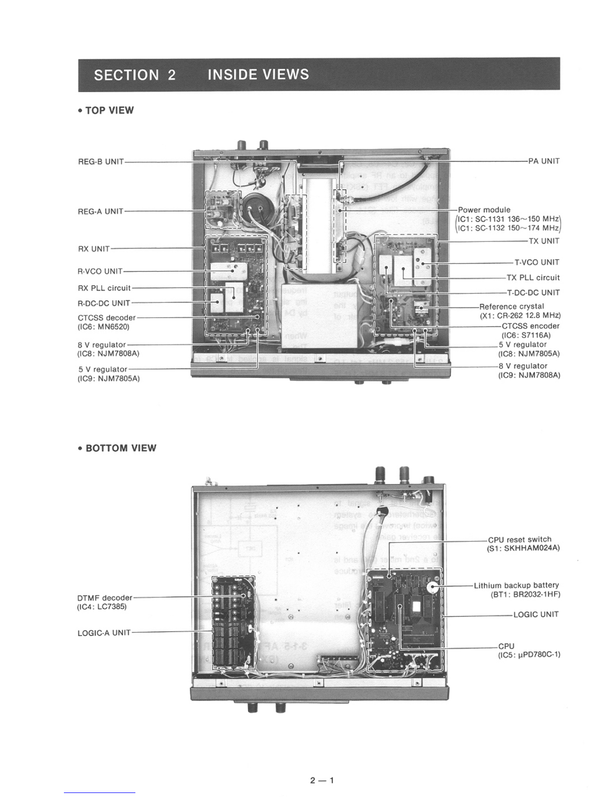
3-1
RECEIVER CIRCUITS
3-1-1 RF CIRCUIT (RX UNIT)
Received signals enter the antenna connector (J6) and
pass through a bandpass filter (Cl, C2, C4-C6, C8, L1,
L2). The filtered signals are applied to an RF amplifier
(Ql). The RF amplifier (Ql) employs an FET (3SK121)
which expands the dynamic range with low noise. The
RF signals are applied to a bandpass filter (C14, C15,
C17-C19, C21--C23, C25, L4-L6).
3-1-2
I
st MIXER AND 1st IFCIRCUITS
(RX UNIT)
3-1-4 SQUELCH CIRCUIT
(RX AND LOGIC UNITS)
A squelch circuit cuts out AF signals when no RF signal
is received. By detecting noise components in the AF
signals, the squelch circuit switches the AF mute
switches.
Some noise components in the AF signal from IC1 (pin 9)
are applied to an active filter section (IC1, pin 10) via a
de-emphasis circuit (R26, C51-C53). This circuit is
an integrated circuit with frequency characteristics of
-6 dBloctave. The [SQUELCH] control (R2) on the
FRONT PANEL adjusts the IC1 (pin 10) input level.
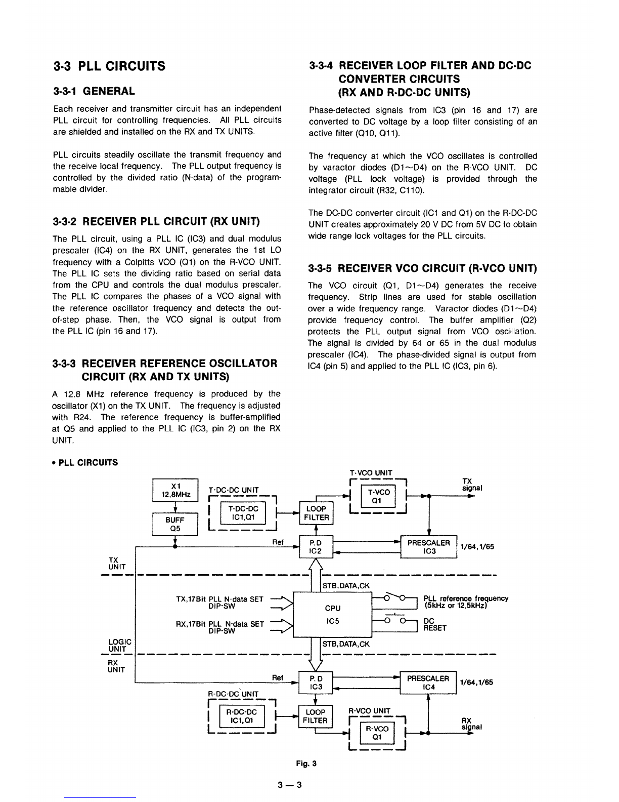
The 1st mixer circuit converts the received signals to a The active filter section amplifies noise components of
fixed frequency of the 1st IF signal with a PLL output frequencies of 20 kHz and above and outputs the result-
frequency. By changing a PLL frequency, only the ing signals from pin 11. Output signals are rectified
desired frequency can be passed through a pair of by D4 and D5 and are then converted to DC voltage.
crystal filters at the next stage of the 1st mixer. When the rectified noise voltage is "HIGH", Q5 turns ON.
The filtered signals are applied to a 1st mixer ((22) and The collector of Q5 outputs the squelch signal. The
are then mixed with a 114.2 MHz-152.2 MHz 1st LO signal is applied to IC9 (pin 16) on the LOGIC UNlT
signal from the PLL circuit to produce a 21.8 MHz 1st IF through the "SQL-S" signal line.
signal. When the rectified noise voltage is "LOW", Q5 turns
The 21.8 MHz 1st IF signal is applied to FI1. FI1 is OFF. The collector of Q9 outputs the busy signal. The
an MCF (Monolithic Crystal Filter) which suppresses out- signal is applied to the [BUSY] indicator on the LED UNlT
of-band signals. The 1st IF signal is applied to a 1st IF through the "BUSY" signal line. The [BUSY] indicator
amplifier (Q3). lights up in green.
2nd
IF
AND
DEMODULATOR CIRCUITS
3-1-3 2ndIFAND DEMODULATORCIRCUITS
(RX UNIT)
The 2nd mixer circuit converts the 1st IF signal to
a 2nd IF signal. A double superheterodyne system
(which converts receive signals twice) improves the image
rejection ratio and obtains stable receiver gain.
The amplified signal is applied to a 2nd mixer (Q4) and is
then mixed with a 21.345 MHz 2nd LO signal to produce
a 455 kHz 2nd IF signal.
The 455 kHz 2nd IF signal is applied to a ceramic filter
(F12) where unwanted signals are suppressed and then
to a limiter amplifier section in IC1 (pin
5).
2nd
Mix
signal
I
-
-
X2
52
455.0kHz
,
7
I
6 5
4
DET
OSC
IC1
Active
9
10
-
SQL
output
IC1 contains the local oscillator circuit, limiter amplifier,
3-1-5 AF AMPLIFIER CIRCUIT
quadrature detector circuit, and active filter circuit. The
(RX AND AF UNITS)
local oscillator section and XI generate 21.345 MHz for ~h,
AF
signal output from 1~1
(pin 9) is applied to a
the 2nd LO signal. monolithic IC (IC2, pin 3) which functions as a high-pass
and low-pass filter. The filtered signal is output from
The 2nd IF signal from the limiter amplifier (IC1, pin 5) IC2 (pin 7) and is then applied to the [VOLUME] control
is applied to the quadrature detector section (IC1, pin 8 (131) on the FRONTPANEL through an AF mute switch(Q6).
and ceramic discriminator X2) to demodulate the 2nd when the squelch is closed, Q6 cuts
off
the
AF
signal as
IF signal into an AF signal. The AF signal is output an AF mute switch. The AF signal is power-amplified
from IC1 (pin 9). at an AF power amplifier (IC1) on the AF UNIT to drive
a speaker.