Kirisun DP770 User manual


DP770 Service Manual
Contents
1.General Introduction...................................................................................................................................3
1.1. Scope.......................................................................................................................................................................3
1.2. Safety Precaution...................................................................................................................................................3
2.External View and Functional Keys..........................................................................................................4
2.1. External View and Functional Keys.....................................................................................................................4
2.2. LED Indicator..........................................................................................................................................................5
3.Circuit Description......................................................................................................................................6
3.1. RF Section...............................................................................................................................................................6
3.1.1. Transmitter Circuit..................................................................................................................................6
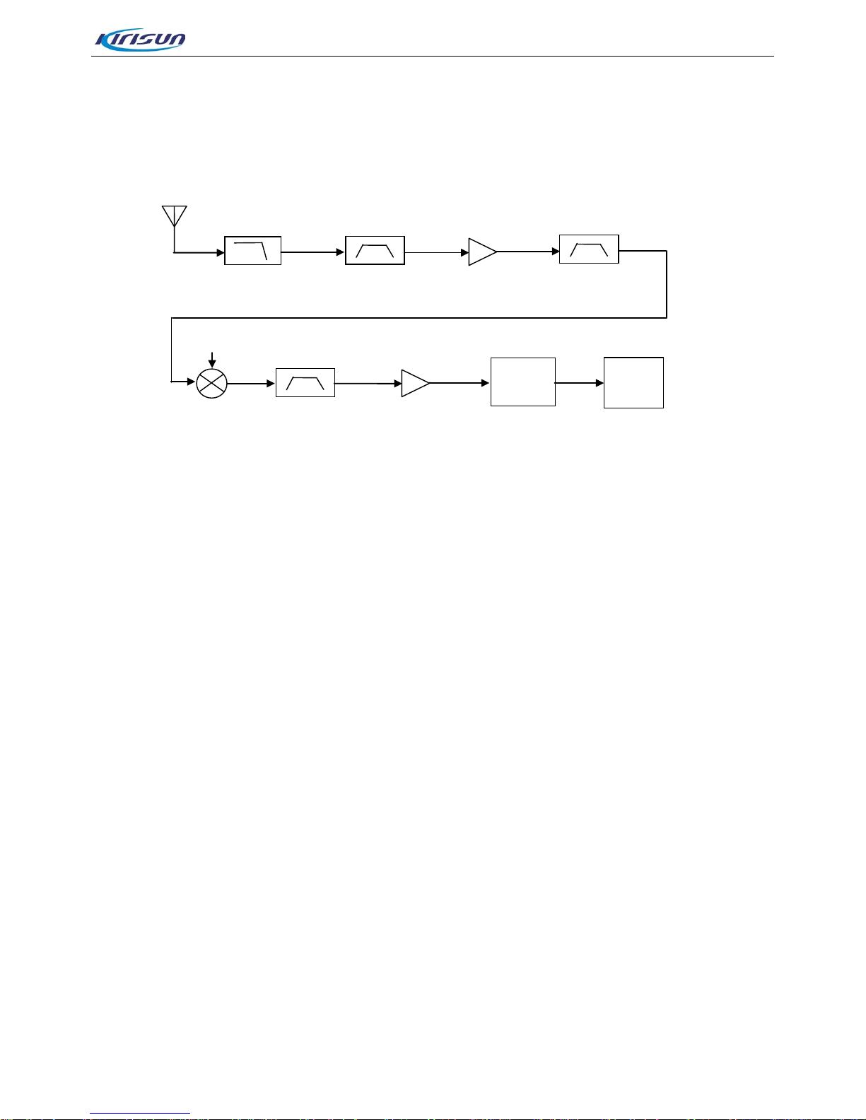
3.1.2. Receiver Circuit .....................................................................................................................................8
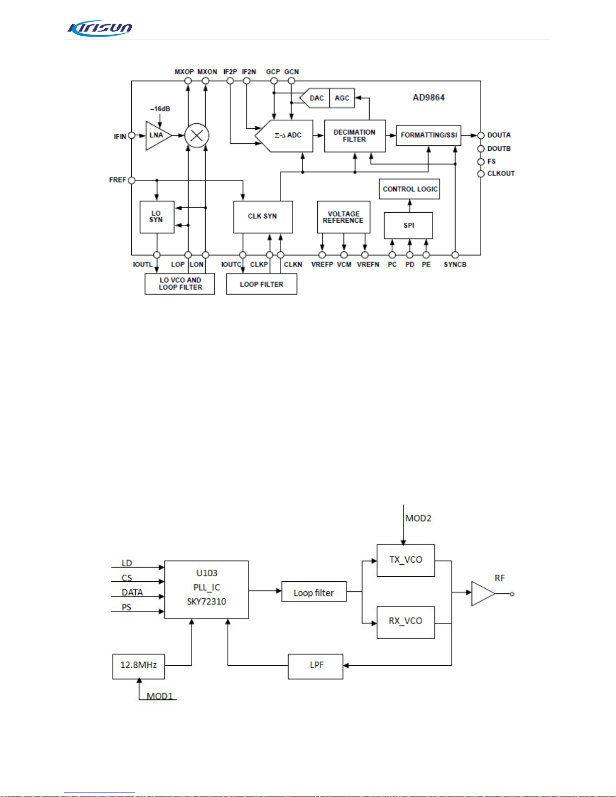
3.1.3. Frequency Generation Unit ...................................................................................................................9
3.1.4. GPS Circuit..........................................................................................................................................10
3.2. Baseband Section................................................................................................................................................11
3.2.1. Power Section...................................................................................................................................... 11
3.2.2. Audio Section....................................................................................................................................... 11
4.Function Instruction and Parameters Setting .......................................................................................13
4.1. General Functions................................................................................................................................................13
4.2. Parameters Setting..............................................................................................................................................14
5.Assembly and Disassembly ....................................................................................................................17
5.1. Attaching and Detaching the Battery.................................................................................................................17
5.2. Attaching and Detaching theAntenna...............................................................................................................18
5.3. Attaching and Detaching the Belt Clip...............................................................................................................19
5.4. Detaching the Chassis.........................................................................................................................................19
5.5. Removing the PCB board from the Chassis....................................................................................................20
5.6. Detaching the Keypad Board from the Case....................................................................................................20
5.7. Exploded View......................................................................................................................................................22
6.Tune Mode .................................................................................................................................................25
6.1. Required parts in adjustment..............................................................................................................................25
6.2. Adjusting and checking method.........................................................................................................................25
Page 1 of 102

DP770 Service Manual
6.2.1. Frequency description.........................................................................................................................25
6.2.2. Adjustment Equipments.......................................................................................................................26
6.2.3. Adjustment instruction of TX................................................................................................................26
6.2.4. Receiver section adjustment instruction..............................................................................................28
6.2.5. GPS Performance Test Instruction......................................................................................................30
7.Main Specifications ..................................................................................................................................31
8.Repairing and Testing Equipments.........................................................................................................33
9.Basic Troubleshooting.............................................................................................................................34
Appendix 1 Material List(Electrics Parts)400-470MHz.........................................................................36
Appendix 2 Material List(Electrics Parts)136-174MHz.........................................................................54
Appendix 3 Material List (Structural Section)...........................................................................................66
Appendix Figure 1 DP770 UHF Main Board Top Side PCB View.............................................................69
Appendix Figure 2 DP770 UHF Main Board Bottom Side PCB View......................................................70
Appendix Figure 3 DP770 UHF Keypad Top Side PCB View...................................................................71
Appendix Figure 4 DP770 UHF Keypad Bottom Side PCB View.............................................................72
Appendix Figure 5 DP770 UHF Main Board Schematic Diagram............................................................73
Appendix Figure 6 DP770 UHF Keypad Schematic Diagram...................................................................85
Appendix Figure 7 DP770 VHF Main Board Top Side PCB View.............................................................86
Appendix Figure 8 DP770 VHF Main Board Bottom Side PCB View ......................................................87
Appendix Figure 9 DP770 VHF Keypad Top Side PCB View ...................................................................88
Appendix Figure 10 DP770 VHF Keypad Bottom Side PCB View...........................................................89
Appendix Figure 11 DP770 VHF Main Board Schematic Diagram..........................................................90
Appendix Figure 12 DP770 VHF Keypad Schematic Diagram...............................................................102
Page 2 of 102

DP770 Service Manual
1.General Introduction
1.1.Scope
This manual is used for maintenance and repairing of the DP770 digital handheld radio, and intended to be
used by experienced technicians and trained engineers. Changes may occur with the technology
development. To require latest technology development information, please contact our company or the
local dealer.
Before any repairing, please read this manual carefully.
1.2.Safety Precaution
Electromagnetic Radiation Energy of Radio
Radios will generate and radiate electromagnetic energy, and Kirisun Radios’ electromagnetic radiation
meets the demand of domestic and international standards. To ensure optimum efficiency of the radio and
reduce electromagnetic radiation, when using the radio, it should be perpendicular to the ground. Keep
your mouth 2-5cm away from the microphone.
Electromagnetic Interference
To avoid interference, please turn off the radio in the site which specifically forbids using radio, e.g. hospital,
airport, health center and etc.
Explosive harmful gases
In the place with explosive harmful gases, such as the lower deck of a hull, fuel or chemical storage,
transportation facilities, places that contain chemicals or dust particles or metal powder in the atmosphere,
radio should be shut down.
When getting close to the blast zone and detonator electric, radio should be turn off.
Charging or replacing battery is not allowed in the place with potential explosive gases.
Antenna Damage
Do not use the radio when the antenna is broken, which will cause a mild burn to your skin.
Replacing Spare Parts
Please try not to replace the spare parts which are not contained in the spare part list.
Page 3 of 102

DP770 Service Manual
2.External View and Functional Keys
2.1.External View and Functional Keys
No. Part Name No Part Name
A Antenna B
Volume/Channel Knob
Rotate the knob to adjust the
volume.Short press the key, the
feature of the knob switches from
adjusting the volume to changing
the channel.
C LCD Display
160*128, 65K colors, 1.8 TFT
LCD. D
Universal Connector for
Accessories
Connect USB programming cable,
earphone or some other
accessories.
E
Top Key (TK)
Programmable, default: short
press to enable emergency alarm,
long press to exit emergency
alarm.
F LED Indicator
G Side Key 1 (SK1)
Programmable, default: none. H PTT Key
I Side Key 2 (SK2) J Left Key
D
M
N
O
P
G
H
J
K
I
L
R
Q
E F
A
B
C
Page 4 of 102

DP770 Service Manual
Programmable, default: none. Press the key to select the items
shown at the bottom left of the
screen.
K Dial Key
Press the key to send data or text
messages. L 4-way Navigation Key
M
Right Key
Press the key to select the items
shown at the bottom right of the
screen.
N
ON/OFF/Hookoff Key
Return to the standby screen.
Long press the key to turn on/off
the radio.
O Numeric keypad P MIC
Q Speaker
2.2.LED Indicator
•Red LED glows: Radio is transmitting.
•Green LED glows: Radio is receiving (voice, short message, or data) or there is an activity on the
channel.
•Orange LED glows: This means the call hang time period. That is, you can press PTT to talk while the
orange LED glows
•Orange LED flashes: Radio is in emergency status; or there is a missed call / incoming call alert; or the
radio is scanning.
•Red LED flashes: Radio is receiving emergency alarm or "power on check" failed.
Page 5 of 102

DP770 Service Manual
3.Circuit Description
3.1.RF Section
Figure 3-1 RF Schematic Diagram
3.1.1. Transmitter Circuit
Figure 3-2 Transmitter Circuit Diagram
Pre-Driver2 Drive-stage Final-stage Tx/Rx Switch Low-pass Filter
Microstrip
Matcher
APC
To RX
Gate voltage control
Subtracter
Sampling
resistor
BATT+
I/V
convertor
Attenuator
To GPS
TEMP
Sensor
Close To Final PA
Temp Det Level
Antenna
FGU
Pre-Driver1
Page 6 of 102

DP770 Service Manual
The transmitter circuit includes three parts:
•Transmitter Power Amplifier
The carrier signal generated by the TX VCO is modulated and amplified, and feeds to the transmitter circuit
via the following steps.
Step1: The signal passes a Π-type attenuator, realizing segregative isolation between RF power amplifier
circuit and TX VCO.
Step2: The signal are pre-amplified by a pre-driver amplifier (UHF: Q301, VHF: Q72), providing further
segregative isolation between itself and the next level amplifier.
Step3: The signal goes to the next pre-amplifier and drive amplifier (RD01) to obtain further amplification,
guarantying to provide enough driver power signal to the final-stage amplifier (RD07) and obtain the final
power amplification..
Step4: After amplified by multiple amplifiers, the transmitter signal is processed by a microstrip line to
complete output impedance matching at the output of final-stage amplifier, to reduce the output loss caused
by impedance mismatch.
Step 5: The transmitter signal goes through the RX/TX switch and enters to the low-pass filter.
•Low-pass Filter Circuit of suppressing the harmonics
The low-pass filter is high-grade low-pass filter composed of lumped-parameter inductors and capacitors.
By this filter, the spurious signal within the stop band can be attenuated as much as possible while the
in-band ripple is within the required range.
•Auto Power Control Circuit (APC includes temperature detection circuit)
In the auto power control and temperature detection circuit, the drain current from the driver amplifier and
final-stage amplifier is converted to voltage via the sampling resistor and subtraction circuit which is
composed of the first operational amplifier.
This voltage is compared with theAPC control voltage of output by DAC at the second operational amplifier.
Then the error voltage controls TX power by controlling the bias voltage at the gate of amplifier (including
the driver amplifier and the final-stage amplifier. The temperature sensor IC detects the surface
temperature of the final-stage amplifier, and converts it to DC voltage. Then the DC voltage is compared
with the voltage corresponding to the protection temperature (generally 80% of the extreme temperature) of
the amplifier. If the temperature is too high, the bias voltage of the amplifier will be reduced until the surface
temperature falls below the protection temperature.
Page 7 of 102

DP770 Service Manual
3.1.2. Receiver Circuit
Figure 3-3 Receiver Circuit Diagram
The receiver circuit mainly comprises RF band-pass filter, low-noise amplifier, mixer, IF filter, IF amplifier
and IF processor.
•Receiver Front-end
The HF signal from the low-pass filter passes through the electrically tunable band-pass filter controlled via
APC/TV1 level, to remove out-of–band interference signal and to send wanted band-pass signal to the
low-noise amplifier (UHF:Q205,VHF:Q62). The amplified signal goes to a band-pass filter controlled via
TFV level to remove out-of-band interference signal generated during amplification, and to send wanted HF
signal to the mixer (UHF:Z201,VHF:Z10).
Meanwhile, the first local oscillator signal generated by VCO passes through the low-pass filter and also
goes to the mixer (UHF: Z201, VHF: Z10). In the mixer, the wanted signal and the first local oscillator are
mixed to generate the first IF signal (UHF: 73.35MHz, VHF: 51.65MHz). The signal passes a frequency
selective network composed of LC, to suppress carrier other than the first IF signal, and to increase the
isolation between the mixer and the IF filter. After that, the first IF signal is processed by the crystal filter
(UHF: Z202, VHF: Z11) and is sent to the two-stage IF amplifier circuit composed of 2SC5006 for
amplification. Then the amplified signal goes to the IF processor AD9864 (UHF: U201, VHF: U91) for
processing.
•eceiver Back-end
Figure 3-4 IF Processor Diagram
AD986
Antenna
OMAP13
Low-pass filter
Insertion loss = -1dB
-120dBm
-121dBm
Band-pass filter
Insertion loss = -3dB
-124dBm
Band- pass filter
Insertion loss = -3dB
-109dBm
Low noise amplifier
Gain = 18dB
-106dBm
Lo: 0dBm
-115dBm
Mixer
Insertion loss = -6dB
Crystal filter
Insertion loss = -6dB
IF amplifier
Gain = 25dB
Po-1dB = -24dBm
-121dBm
Clip at -24dBm
-96dBm
Point A
Point B
Page 8 of 102

DP770 Service Manual
The first IF signal (73.35MHz) output by the IF amplifier goes into AD9864 (UHF: U201, VHF: U91) via Pin
47 and completes the second mixer, where the signal is converted to the second IF signal (2.25 MHz). The
second IF signal is converted to digital signal via ADC sampling, and output via the SSI interface. Finally,
the digital signal is sent to DSP (OMAP138) for demodulation.
AD9864 employs reference frequency of 12.8MHz. The second local oscillator is composed of an external
oscillator, a varactor and some other components, to provide the (UHF: 71.1MHZ, VHF: 49.4MHz)
71.1MHz LO signal. The 18MHz clock input frequency of AD9864 is generated by the LC resonance loop.
3.1.3. Frequency Generation Unit
Figure 3-5 Frequency Generation Circuit Diagram
Page 9 of 102

DP770 Service Manual
The frequency generation circuit is composed of VCO and PLL. It is the core module of the whole TX-RX
system. This circuit provides accurate carrier frequency during transmission; and provides stable local
oscillator signal during reception. It has a direct influence on the performance of the system.
•Working Principle of PLL
The 12.8MHz frequency generated by the reference crystal oscillator goes to PLL for division, generating
the reference frequency (i.e step frequency f1). The frequency generated by VCO is filtered harmonic via
LPF and generates another frequency (f2) through the frequency divider in PLL. Then frequencies f1 and f2
are compared in the phase detector (PD), to generate continuous pulse current. The pulse current goes to
the loop filter for RC integration and is then converted to CV voltage. Then the CV voltage is sent to the
varactor of VCO. It adjusts the output frequency of VCO directly until the CV voltage becomes constant.
Then the PLL is locked, and the stable frequency output by VCO goes to the TX-RX channel after passing
through two buffer amplifiers.
•Working principle of VCO
Voltage controlled oscillator applies oscillation mode of three-point capacitance, and gains different output
frequency through changing controlled voltage (CV) of varactor. Rx VCO is composed of oscillating circuit
and Q24/Q29 and provides local oscillation signal. Tx VCO is composed of oscillating circuit and Q27/Q28
and provides carrier of Tx signal.
Working principle employs colpitts oscillator circuit (the RX oscillator circuit is composed of D102, D103,
D106, D107 and L112 (VHF:D32, D33, D36, D34 and L23); the TX oscillator circuit is composed of D108,
D109, D110, D101and L117 (VHF:D38, D39, D40, D41 and L31). It obtains different output frequencies by
changing control voltage of varactor (i.e.CV voltage).RX VCO is composed of oscillator loop and Q104
(VHF:Q43), providing local oscillator signal. TX VCO is composed of oscillator loop and Q108 (VHF Q44)
and provides carrier of TX signal.
•Two-point Modulation
To obtain higher modulation accuracy and lower 4FSK bit error, it employs two-point modulation technology
in the TX mode. MOD1 and MOD2 send the modulation signal to the modulation end of VCO and the
reference crystal oscillator of PLL respectively to modulate TX VCO and the reference crystal oscillator.
3.1.4. GPS Circuit
Figure 3-6 GPS Circuit Diagram
The GPS function is realized via REB-1315LPx (GPS module).The GPS module integrates a baseband
processor, a LAN and a SAW.The GPS function is realized via the following steps:
Page 10 of 102

DP770 Service Manual
Step1: The 1575.42MHz GPS signal is received by the antenna, and then goes to HPF to remove the
in-band signals used for transmission and reception.
Step2: The signal goes to GPS module for amplification and filtering after frequency selection via filter.
Then it will be sent to baseband section for calculation.
Step3: The calculated GPS position information is sent to OMAP for processing via the UART interface.
Meanwhile, OMAP138 can send appropriate command information to the GPS module via the UART
interface.
Step4: Finally, the OMAP sends the processed data information to the LCD.
3.2.Baseband Section
3.2.1. Power Section
Figure 3-7 Power Section Diagram
The radio adopts 7.4V li-ion battery as power supply. The baseband and RF circuit are supplied by
independent power structure. The baseband power is composed of two stage conversion circuit. The first
stage reduces the battery voltage to 5V by DC/DC, and the second stage converts the 5V voltage to power
required voltage for the system by the power management.
Power On/Off: Power On/Off is implemented through a PMOS component. When the Power On/Off key is
pressed, PWR_Key signal becomes high level, and PMOS component becomes conducted. The system
will begin initialization and set Soft_ctr to be high level. Thus, the radio is powered up. During the power off
process, when the system detects that the Power On/Off key is pressed, the system will begin executing
the shut down operations, and finally set Soft_ctr to be low level, which will shut down the PMOS
component, thus the radio being powered off.
3.2.2. Audio Section
The audio module is mainly for audio input and output. It uses TLV320AIC14 as audio codec to convert and
PMU
VCC_3V3
VCC_1V8
VCC_1V2
LDO_3V3
VCC_5V0
Power switch
DC/DC
Battery
Audio PA
Soft_ctr
PWR_Key
RF_PWR
Logic OR
LDO
GPS_3v3
RTC_1v2
Page 11 of 102

DP770 Service Manual
process audio signal and digital signal. The audio amplifier TDA8547TS is used to amplify the analog audio
signal.
DSP processes digital signal (i.e audio signal encoding/decoding, digital I/Q signal decoding, digital audio
signal processing). The AD9864 converts and processes the RF IF, and sends un-demodulated serial
digital signal to the DSP for processing. Then DAC5614 converts the digital signal output by DAS to analog
signal.
Figure 3-8 Audio Section Diagram
CODEC Audio PA
OmapL138
AD9864
TLV5614 Baseband signal
Configure data
RX signal RX
TX
IICIIS
INT_MIC
EXT_MIC
Voice signal
INT_SPK
Interface EXT-SPK
TONE
Mode
select
SPI
MIC
Input
PWM
Control
signal
•Diagram of Signal Flow
The microphone converts the audio signal into electrical signal, which is amplified by PGA of the codec and
then sent to ADC of the codec for sampling. After digital audio processing, the signal is output DSP for
processing. Then the signal is sent to DAC (TLV5614), which converts the signal to modulation signal. After
modulated and amplified in the RF module, the signal is sent out from the antenna.
The RF signal received by the RF module is converted to digital byADC (AD9864), and is then sent to DSP
for modulation and processing. Then the digital signal is sent to the digital audio processor of the codec for
digital audio processing, and is then converted into analog audio signal by DAC of the codec. Finally the
signal is amplified by the external audio amplifier (TDA8547TS) to drive the speaker.
•System Peripheral Function Unit
The system peripheral consists of analog/digital converter module, vocoder encryption module, TF card
interface module, display module, key detection module and acceleration sensor module. These modules
are used to achieve human-radio interaction, state detection, communication encryption and feature
extension. The analog/digital converter is used for voice signal strength detection, power supply detection,
temperature detection, so as to realize VOX, low battery warning and temperature control. The acceleration
sensor is used to detect tilted state, realizing mandown function. The TF card module interface is used for
communication encryption, to provide communicate security.
Page 12 of 102

DP770 Service Manual
Figure 3-9 The Composing of System Basic Peripheral
ADC
Voice level detect
Codec
Accelerometer
TF card
IIC0
INT_MICEXT_MIC CVDECT Voltage Temperature
detect
IIC1
GPS
UART0
OmapL138
Key scan module
LCD
LCD
controler
4.Function Instruction and Parameters Setting
4.1.General Functions
•Support P-Call, G-Call,A-Call in digital mode.
•Support P-Call, G-Call,A-Call in analog mode.
•Support Transmit Interrupt function in digital mode.
•Support Encryption of both voice and data.
•Support Short message, status message and GPS data information.
•Support Stun, Un-kill, Remote Monitor, Call Alert digital signaling.
•Support Self-defined Kill digital signaling.
•Support CTCSS/CDCSS in analog mode.
•Support MDC1200, 2 Tone, DTMF, 5Tone signaling system in analog mode.
•Support Emergency function.
•Support scan function of digital channel, analog channel and mixed digital and analog channel.
•Support the maximum of 1024 channels capacity.
•Support the maximum of 248 Zones and the maximum of 128 channels in every zone.
•Support the maximum of 512 contacts.
•Support graphic menu operation interface.
•Support LED, choices of alert tones and vibration indication.
•12.5 kHz, 20 kHz or 25 kHz channel spaces can be chosen by PC software.
•Real-time display of signal strength.
•Support battery display and low battery alarm alert functions.
Page 13 of 102

DP770 Service Manual
4.2.Parameters Setting
Radios have default parameters. While users can set parameters of frequency, channels, function of
scanning or encryption, etc according your own requirements.
•Parameters setting steps as follow:
Step 1. Install the right version of Kirisun CPSp.
Step 2. Connect radio with computer by Kirisun programming cable.
Step 3. Make sure radio’s power is on.
Step 4. Execute CPSp and start operation.
•CPSp installation steps as follow:
Step 1. Double click the installation file; pop-up interface as Figure 4-1.
Figure 4-1
Step 2. Click “Next” and enter into the next interface to choose the installation route.
Step 3. In the interface shown in Figure 4-2, users can click “Browse” to choose the installation route, or
use the default route, and click ”Next” to enter the next interface to choose language.
Figure 4-2
Page 14 of 102

DP770 Service Manual
Step 4. Click “Next” to enter into installation information confirmation interface.
Figure 4-3
Step 5. Click “Next” to enter into the finished interface.
Figure 4-4
Page 15 of 102

DP770 Service Manual
Step 6. Click “Finish” to finish installation.
Figure 4-5
Step 7. After successful installation, double click the software, as shown in Figure 4-6
Figure 4-6
Page 16 of 102

DP770 Service Manual
Users can read the radio’s date, or revise the data and then write into the radio.
Please refer to the help file in the CPSp for the detailed operation instruction about Kirisun CPSp.
Notes:
Errors of parameter configuration may make certain functions cannot be used properly, in general, which
can be solved by writing the correct parameters configuration.
Before parameter configuration modification, we strongly recommend backup the current parameters,
make sure that the radio can restore after an error occurs.
5.Assembly and Disassembly
5.1.Attaching and Detaching the Battery
Attaching the battery as shown in figure 5-1.
Put the battery into radio’s aluminum alloy bracket slot.
Push up until a click is heard.
Figure 5-1
Page 17 of 102

DP770 Service Manual
Detaching the battery as shown in Figure 5-2
Push up the battery buckle at the end of the battery.
Pull down to detach the battery.
Figure 5-2
5.2.Attaching and Detaching the Antenna
As shown in Figure 5-3, put the antenna into radio’s thread hole,
and rotate clockwise to fasten it.
Figure 5-3
As shown in Figure 5-4, rotate counter-clockwise to detach.
Figure 5-4
Page 18 of 102

DP770 Service Manual
5.3.Attaching and Detaching the Belt Clip
As shown in Figure 5-5, align the screw holes on the belt clip, which is
located on the back of the radio, and fasten them with the screwdriver.
Figure 5-5
As shown in Figure 5-6, unfasten the screws to detach the belt clip.
Figure 5-6
5.4.Detaching the Chassis
Step 1. Detaching the belt clip (Figure5.6);
Step 2. Removing the antenna (Figure 5.4);
Step 3. Removing the battery (Figure 5.2);
Step 4. Removing the two screws on the bottom of the chassis. Remove the
two screws on the side of shell, and remove the nut from antenna
connector.
Figure 5-7
Page 19 of 102
Other manuals for DP770
4
Table of contents
Other Kirisun Radio manuals

Kirisun
Kirisun PT6808-02 User manual

Kirisun
Kirisun PT8000 User manual

Kirisun
Kirisun V688-02 User manual

Kirisun
Kirisun PT8200 User manual

Kirisun
Kirisun DP405 User manual

Kirisun
Kirisun DP990 User manual

Kirisun
Kirisun FM540 User manual

Kirisun
Kirisun PT8100 User manual

Kirisun
Kirisun TM840 Instruction manual

Kirisun
Kirisun DM588-01 User manual

Kirisun
Kirisun PT8000 User manual

Kirisun
Kirisun PT810001 User manual

Kirisun
Kirisun PT810003 User manual

Kirisun
Kirisun FP420 User manual

Kirisun
Kirisun TM840 User manual

Kirisun
Kirisun FP460 User manual

Kirisun
Kirisun M50 User manual

Kirisun
Kirisun PT8100 -01 User manual

Kirisun
Kirisun PT4208 User manual

Kirisun
Kirisun DM588 User manual