UL
CK
DT
UL
PLL IC
IC3
QT TCXO
5V
LOOP FILTER
RIPPLE
FILTER
VCO
Q6
BUFF
Q1 Q2
RF AMP VCO OUT
5V Q14
2ND LOCAL
MB15E03SL MOD
16.8MHz
X1
TCXO
3.5V
TX
VCO
Q14
RX
8R
Q11
*3 2ND LOCAL AMP
Q7
BUFF
5V
4
SPEAKER
IC6
Q33
SW
AF POWER AMP
IC7
AF OUT
MUTE
TDA1519C
IC8A IC8BIC8CIC8D
AMP LP LP AMP CTCSS/DCS
MIC
IC9C IC9BIC9AIC9D
AMP HP LP LP HP
Q26 8R
IC10BIC10A
HP AMP 2T
IC5
DTMF
DECODER
D0
D1
D2
D3
DV
J1 SPK
IC13D IC13AIC13BIC13C
LP LP IDC AMP
MOD
VR1
10K
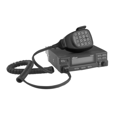
PT8000 SERVICE MANUAL
Front End of Receiver
Signals from the antenna are filtered by BPF which consists of two-LC via
RX/TX switch (D3 D11). After being filtered out the useless out-of-band
signals, the signals are amplified by LNA consisting of Q18 and external
components.
Signals from LNA are filtered again by BPF which consists of three-LC
before entering the 1st mixer (Q19).
AGC Circuit
It consists of Q16 and peripheral circuit. AGC will work to reduce the gain
of Q18 only when the input signal is oversize.
1st mixer
The first IF (49.95MHz) signal is produced after mixing of the receiving
signal from LNA and the 1st local oscillation signal from frequency
synthesizer.
IF Circuit
The first IF signal is filtered out adjacent channel and other useless signals
by crystal filter (XF1).
The first IF signal from crystal filter is amplified bythe firstIF amplifier (Q20)
before processing of IC in IF( IC6 TA31136).
IF IC consists of the 1st mixer, IF amplifier, limiter, frequency discriminator,
noise amplifier, audio low pass filter.
Signals (16.8MHz) from X1 are amplified by Q11 and peripheral circuit and
then generatethe second localoscillator (50.4MHz).The secondIF signals
(450kHz) are generated after signals mixing of the second local oscillation
(50.4MHz)and thefirst IF (49.95MHz)inIC6. Audiosignals aredemodulated
and outputted by IC6 after the second IF signals are amplified and limited
in IC6 and then filtered by ceramic filter(CF1 or CF2 450kHz).
The second IF filter selective circuit consists of CF1, CF2, D20, D21 and
peripheral circuit. When vehicle station is set on broadband, CF2 is
connected and CF1 is cut off; when it is narrowband, CF1 is connected
and CF2 is cut off.
Squelch Circuit
Signals demodulated by IC6 are amplified by noise amplifier of IC6 and
then amplified further by Q21. After that, the signals are demodulated by
D25, and then the generated DC level enters squelch circuit controlled by
MCU. The voltage is in inverse proportion to the input signals.
3.3 Principles of Transmitter (TX)
Transmitter Power Amplifier
VCO RFAMP
8T 8R
Q4 Q5
DRIVE
PRE
8T 8T
ANTSW LPF
APC CONTROL
IC4
TX/RX SW
TOANT
IC1
RA30H
APC
8T
13.8V
The modulated RF signals from VCO are amplified by Q1, Q2, Q4 and Q5
before the power amplification in IC1. IC1 Output Power: 25W
Gate bias of IC1 is controlled by APC circuit, so the output power of
transmittercan be controlled conveniently bychanging thegate biasvoltage.
APC Automatic Power Control Circuit
The output power of RF power amplifier is detected and converted into DC
level by RF detector diode (D9, D10). The DC level is then compared with
signals from MCU and amplified in IC4 before power output control in Ic1
gate.
The voltage detected by detector diode will increase with oversized output
power of transmitter. When the output voltage of IC4 decreases, the bias
Figure 3.3 Schematic Diagram
for Power Amplifier and Antenna Switch
voltage of IC1 will decrease, finally the output power of transmitter will
decreaseor vice versa. Thus, theoutput powerof transmitterwill keepstable
under any different working condition.
MCU can set the power by changing the voltage input to IC4.
3.4 Principles of Frequency Synthesizer
Figure 3.4 Schematic Diagram for Frequency Synthesizer
The PT8000 adopts PLL frequency synthesizer.
Frequency synthesizer consists of reference oscillator, voltage controlled
oscillator(VCO), programmable frequency divider (PFD),phase comparator
and low pass filter (LPF).
Transmitting VCO Unit consists of Q6, D1, D4, D5 and D6, etc. D8 is the
modulation circuit of transmitting VCO.
Receiving VCO Unit consists of Q12, D14, D16, D17 and D18, etc.
IC3 (MB15E03SL) is PLL integrated circuit and contains programmable
parametric frequency divider (PPFD), programmable frequency divider
(PFD), phase comparator and charge pump, etc.
Low pass filter consists of R54, C113 and so on.
Reference frequency is provided by X1(TCXO, 16.8MHz).
Reference frequency of TCXO (Temperature-controlled Crystal Oscillator)
isdivided by PPFD in IC3to producereference frequencyof 5kHzor6.25kHz
(controlled by MCU based on the set channel frequency).
The oscillation frequency of VCO is compared with reference frequency to
produce error signal after divided by PFD in IC3. The error signal is filtered
by low pass filter before changing the VCO frequency to the set value in
VCO (it is locking).
Lock lost detection: When PLL is out of lock, IC3 pin14 will output low level
signal to MCU and thenMCU prohibittransmitter fromtransmitting with a
warning tone.
3.5 Audio Processing Circuit:
Figure 3.5 Schematic Diagram for Audio Processing Circuit
MIC Signal Processing:
Voice signals from MIC are amplified in IC13A (IC13Acomposes the AGC
circuit with D32 and Q32 to increase the dynamic range of the circuit), and
thensent to IDC circuit composedby IC13Bafter thepre-emphasis ofC322
and R267. The limited signals are switched broad/narrowband in Q30 and
thenfiltered signals over 3000Hz inthe two-levellow passcircuit composed
byIC13C andD.Thenthe filteredsignals are modulatedto transmittingVCO
by D8 after frequency offset adjustment in VR2.

