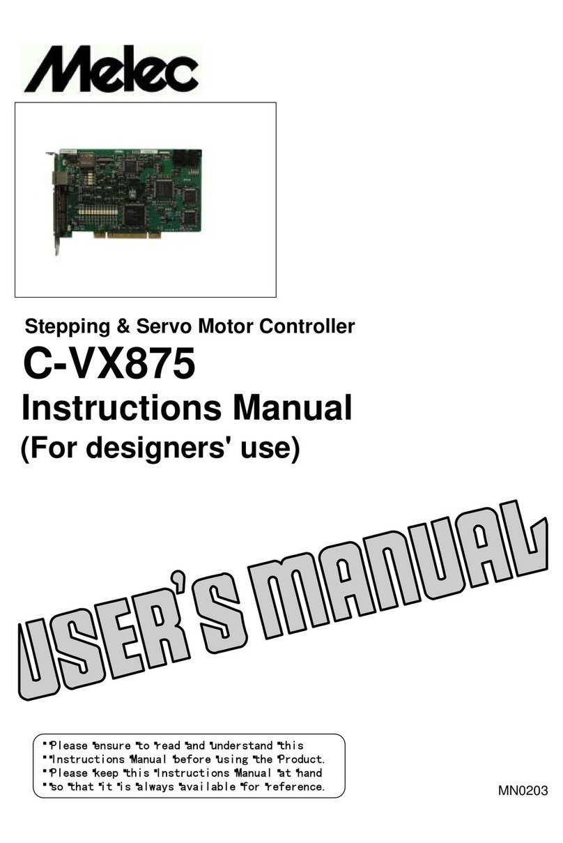
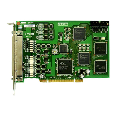
M-Elec C-875 User manual

Stepping & Servo Motor Controller
C-875
Instructions Manual
(For designers' use)
PR0815-1
Please ensure to read and understand this
Instructions Manual before using the Product.
Please keep this Instructions Manual at hand
so that it is always available for reference.

-2-
Introduction
This User's Manual describes the method of dealing with "STEPPING AND SERVO MOTOR CONTROLLER C-875",
which set weight in specification in order to have a product used safely correctly for the designer
of the control system using the stepping motor or servo motor.
Before using this product, carefully read this User's Manual to have a sufficient understanding
of the functions.
Keep this User's Manual on hand so that you can refer to it whenever you want.
Description of Safety
Correct operation procedures are essential.
If you use in a wrong way, an unexpected accident may occur to cause personal injuries
or damage of your properties.
Many of the possible accidents can be avoided if you have a preliminary knowledge about
dangerous situations. For this purpose, this User's Manual describes the precautions if
any dangerous situation can be anticipated.
Such descriptions are given in terms of the following symbols and signal words.
WARNING Death or serious injury may be caused by
incorrect handling.
CAUTION Slight injury or damage of your properties
may be caused by incorrect handling.
Before use
■ This product is not designed for use in the equipment related to nuclear power,
aerospace equipment, vehicles, marine vessels, medical equipment directly in
touch with human body, equipment anticipated to give a serious impact to
properties, and other equipment required to provide high reliability.
■ This product is provided with a LIMIT (overtravel) signal to prevent mechanical
damage.
This signal is an ACTIVE OFF input. Accordingly, even if the system does not
use the LIMIT signal, connect an external power supply for coupler so that the
LIMIT signal may be put into the NORMAL ON state to output pulses.
For details, refer to 14-2.
■ This product is surely used for within this description of the specification method
of this manual, and the limits of specification.
■ Before connecting this product to the expansion slot, certain setting operations must
be done for the circuit board. Refer to the following sections for the setting:
4-2. Board identifier port page 14
10. Initial Specification page 68
11. Interrupts page 69
15-2. Board Shape and Dimensions page 87
■ For details of applied functions referred to in this manual, see the separately issued
the User's Manual [Applied Functions Part].

-3-
Contents
Page.
71.OVERVIEW
2.BASIC CONFIGURATION
2-1. Function Block Diagram 7
2-2. Description of Blocks 8
3.SPECIFICATIONS
3-1. PCI Local bus Specification 9
3-2. Basic Functions 9
3-3. Ratings 10
3-4. Options 10
3-5. Applied Functions 11
4.I/O PORTS
4-1. I/O Port Table 13
4-2. Setting the board identifier port and rotary switch 14
4-3. DRIVE COMMAND PORT 14
4-4. DRIVE DATA1,2,3 PORT (WRITE) 14
4-5. DRIVE DATA1,2,3 PORT (READ) 14
4-6. COUNTER COMMAND PORT 14
4-7. COUNTER DATA1,2,3 PORT (WRITE) 14
4-8. STATUS1 PORT 15
4-9. STATUS2 PORT 16
4-10. STATUS3 PORT 16
4-11. STATUS4 PORT 16
4-12. STATUS5 PORT 17
4-13. General-purpose I/O PORT 17
4-14. I/O INT SET PORT(Additional I/O) 18
4-15. IN10_20INT STATUS PORT(Additional I/O) 18
4-16. IN30_40INT STATUS PORT(Additional I/O) 18
4-17. IN10 PORT(Additional I/O) 19
4-18. IN20 PORT(Additional I/O) 19
4-19. IN30 PORT(Additional I/O) 19
4-20. IN40 PORT(Additional I/O) 19
4-21. OUT10 PORT(Additional I/O) 20
4-22. OUT20 PORT(Additional I/O) 20
4-23. OUT30 PORT(Additional I/O) 20
5.DETAILS OF DRIVE FUNCTIONS
5-1. JOG DRIVE Function 21
5-2. SCAN DRIVE Function 21
5-3. INDEX DRIVE Function 22
5-4. Drive Speed Change Function 22
5-5. Machine Origin Detecting Function (ORIGIN DRIVE) 23
5-6. Machine Origin Detecting Function Using Limit Sensor 23
5-7. S-RATE SCAN DRIVE Function 24
5-8. S-RATE INDEX DRIVE Function 24
5-9. S-RATE DRIVE Parameter Adjusting Function 25
5-10 Slow Stop Function 27
5-11. Fast Stop Function 27
5-12. LIMIT Stop Function 27
5-13. Function for Servo Driver 27
5-14. Current Position Reading Function 27
5-15. Interrupt Request Function 28
5-16. Speed Data Hz Unit Setting Function 28
5-17. DRIVE TYPE Switching Function 29
5-18. Present Speed Reading Function 29
5-19. Set Data Reading Function 29

-4-
6.DESCRIPTION OF BASIC FUNCTION DRIVE
COMMANDS AND OPERATION SEQUENCES
6-1. Basic Function DRIVE Command Table 30
6-2. Special Command Table 31
6-3. NO OPERATION Command 31
6-4. SPEC INITIALIZE1 Command 32
6-5. PULSE COUNTER INITIALIZE Command 33
6-6. ADDRESS INITIALIZE Command 36
6-7. ADDRESS READ Command 36
6-8. SERVO RESET Command 37
6-9. RATE SET Command 37
6-10. LSPD SET Command 37
6-11. HSPD SET Command 38
6-12. DFL COUNTER INITIALIZE Command 39
6-13. SET DATA READ Command 41
6-14. +/-JOG Command 42
6-15. +/-SCAN Command 42
6-16. INCREMENTAL INDEX Command 42
6-17. ABSOLUTE INDEX Command 43
6-18. CSPD SET Command 43
6-19. OFFSET PULSE SET Command 44
6-20. ORIGIN DELAY SET Command 44
6-21. ORIGIN FLAG RESET Command 44
6-22. ORIGIN Command 45
6-23. SRATE SET Command 45
6-24. SLSPD SET Command 46
6-25. SHSPD SET Command 46
6-26. SSRATE ADJUST Command 47
6-27. SERATE ADJUST Command 47
6-28. SCSPD1 ADJUST Command 48
6-29. SCSPD2 ADJUST Command 48
6-30. +/-S-RATE SCAN Command 49
6-31. S-RATE INCREMENTAL INDEX Command 49
6-32. S-RATE ABSOLUTE INDEX Command 49
6-33. ERROR STATUS READ Command 50
6-34. SPEED CHANGE Command 50
6-35. INT MASK Command 51
6-36. PORT SELECT Command 52
6-37. SLOW STOP Command 52
6-38. FAST STOP Command 52
6-39. COUNTER READ 53
6-40. SPEED READ 53
7.MACHINE ORIGIN DETECTING FUNCTION
7-1. Machine Origin Detection Types 54
7-2. ORG-0 Type 55
7-3. ORG-1 Type 55
7-4. ORG-2 Type 56
7-5. ORG-3 Type 56
7-6. ORG-4 Type 57
7-7. ORG-5 Type 57
7-8. ORG-10 Type 58
7-9. ORG-11 Type 59
7-10. ORG-12 Type 59
7-11 Sensor Arrangement 60
7-12. Detecting Conditions 60
7-13. Other Functions 60

-5-
8.DETAILS OF COUNTER FUNCTIONS
8-1. Function Block Diagram 61
8-2. ADDRESS COUNTER Function 62
8-3. PULSE COUNTER Function 62
8-4. DIFFERENTIAL COUNTER Function 63
8-5. Details of COMPARATOR Function 64
9.DESCRIPTION OF PULSE COUNTER AND
DIFFERENTIAL COUNTER COMMAND
9-1. Command Table 65
9-2. PULSE COUNTER PRESET Command 65
9-3. PULSE COUNTER COMPARE REGISTER1 SET Command 66
9-4. PULSE COUNTER COMPARE REGISTER2 SET Command 66
9-5. PULSE COUNTER COMPARE REGISTER3 SET Command 66
9-6. PULSE COUNTER COMPARE REGISTER4 SET Command 66
9-7. PULSE COUNTER COMPARE REGISTER5 SET Command 66
9-8. DFL COUNTER PRESET Command 66
9-9. DFL COUNTER COMPARE REGISTER1 SET Command 67
9-10. DFL COUNTER COMPARE REGISTER2 SET Command 67
6810.INITIAL SPECIFICATIONS TABLE
11.INTERRUPTS
11-1. Interrupt Request Signals upon Termination of Command 69
11-2. Interrupt Request Signal from PULSE COUNTER and DFL COUNTER 69
11-3. Interrupt Request Signal by Input Signals of the Additional I/O 69
11-4. Interrupt Pin Arrangement 69
11-5. Precautions on Using Interrupts 69
12.TIMING
12-1. JOG DRIVE Timing 70
12-2. SCAN DRIVE/S-RATE SCAN DRIVE Timing 70
12-3. INDEX DRIVE/S-RATE INDEX DRIVE Timing 70
12-4. ORIGIN DRIVE Timing 70
12-5. SPEED CHANGE TIMING 71
12-6. DEND Signal Confirmation Timing 72
12-7. SLOW STOP Timing 72
12-8.FASTSTOPTiming(1) 72
12-9.FASTSTOPTiming(2) 73
12-10.LIMIT STOP Timing 73
12-11.EA/EB Clock Input Timing 74
12-12.RDYINT Timing (INTA#) 74
12-13.CNTINT Timing (INTA#) 75
12-14.DFLINT Timing (INTA#) 76
12-15.IOINT Timing (INTA#) 77
12-16.RESET Timing 77
12-17.BUS Timing 78
13.USER CONNECTOR AND I/O CIRCUIT
13-1. User Connector J1, 2 Pin Arrangement 79
13-2. J1 Signal Table 79
13-3. J2 Signal Table (for Additional I/O) 81
13-4. I/O Circuit 82
14.CONNECTIONS
14-1. Connection to the Driver 83
14-2. Connection Examples of a LIMIT Switch or Sensor 84
14-3. Connection Example of the Origin Sensor 84
15.BOARD EDGE CONNECTOR AND BOARD SHAPE
15-1. Board Edge Connector Signal Table 86
15-2. Board Shape and Dimensions 87

-6-
16.CONTROL PROGRAM EXAMPLES
16-1. INITIAL Setting Example 88
16-2. INITIALIZE Program Example 90
16-3. JOG DRIVE Program Example 91
16-4. SCAN DRIVE Program Example 91
16-5. Example of INDEX DRIVE Program Specified in Absolute Value 92
16-6. ORIGIN DRIVE Program Example 93
16-7. PULSE COUNTER Read Program Example 94
9517.TROUBLESHOOTING
18.DATA TABLES
18-1. L-TYPE RATE Data Table 97
18-2. M-TYPE RATE Data Table 97
18-3. H-TYPE RATE Data Table 97
18-4. RATE Curve Graph 97
9919.SAFETY DESIGN PRECAUTIONS
20.C-870v1 ALL COMMAND TABLES
20-1. DRIVE Command Table 100
20-2. Special Command Table 101
21.MAINTENANCE
21-1. Maintenance and Inspection 102
21-2. Storage and Disposal 102

-7-
1.OVERVIEW
The C-875, equipped with Additional I/O(IN:32points,OUT:24points) and 4 independently functioning axes,
is a high performance controller that can bedirectly connected to the PCI bus expansion slot based on
PCI Local Bus Specification Rev. 2.1.
It is designed to offer control for both servo and stepping motors.
Its board is a compact half-size (107 x 170).
Equipped with our high grade chip controller MCC05v2, the pulse generator permits motor control using easier-to-
operate command type.
The multi-function PULSE COUNTER and DIFFERENTIAL COUNTER on the MCC05v2 enable chip controller to count
feedback pulses from a servo driver as well as detecting step-out of a stepping motor with the encoder.
Since the C-875 are provided with the 4 independent axes, the first axis, the second axis, the third axis and
the fourth axis are called X axis, Y axis, Z axis and A axis respectively.
As a rule, the following description will be given about only the X axis.
2.BASIC CONFIGURATION
2-1. Function Block Diagram
X axis MCC05v2
(2)
Drive control block
Counter block
(3)
Y axis MCC05v2
(2)
Drive control block
Counter block
(1) (3) (7)
PCI Bus Bus interface Z axis MCC05v2 User interface
block (2) block
Drive control block
Counter block
(3)
A axis MCC05v2
(2)
Drive control block
Counter block
(3)
(4)
General-purpose I/O block
Input buffer, output buffer
(5)
Additional I/O block
(6)
Board identifier port

-8-
2-2. Description of Blocks
(1) Bus interface block
Interface block with the PCI bus.
This block consists of the interface IC dedicated to PCI bus and a serial EEPROM, etc.
(2) Drive control blocks
These blocks output serial pulses for motor control. The blocks mount pulse generators MCC05v2 for
individual 4 axes, so the 4 axes can be independently driven.
For distinction among the 4 axes, these drive control blocks are called X axis MCC05v2, Y axis MCC05v2,
Z axis MCC05v2 and A axis MCC05v2 respectively.
(3) Counter blocks
This counter block consists of the ADDRESS COUNTER, general purpose PULSE COUNTER and DIFFERENTIAL COUNTER.
The ADDRESS COUNTER is used for counting pulses from the MCC05v2, the general purpose PULSE COUNTER is used
for counting external 90゜phase shifted clocks and the DIFFERENTIAL COUNTER is used for counting deviation
of these pulses.
This block allows to read a counting any time as needed, preset a count or interrupt at any counting
(or deviation level).
(4) General-purpose I/O block
This block is provided with 4 inputs and 4 outputs isolated by photo coupler.
Because of a +24V coupler interface, it can control relays and solenoid valves.
The host controls this block completely independent of the other blocks.
(5) Additional I/O block
This block is provided with 32 inputs and 24 outputs isolated by photo coupler.
Because of a +24V coupler interface, it can control relays and solenoid valves.
4 of 32 inputs can generate an interrupt at the time of ON or OFF.
The host controls this block completely independent of the other blocks.
(6) Board identifier port
When more than two C-875s are used, the boards must be numbered. This is used only for the port.
(7) User interface block
Interface block for signals of the servo/stepping motor drivers and sensors, etc.

-9-
3.SPECIFICATIONS
3-1. PCI Local Bus Specification
(1) PCI Local Bus Specification Rev. 2.1
(2) Bus interface
32 BIT BUS(inside 8 BIT), 5V signaling environment, 33MHz clock
(3) PCI configuration register
31 16 15 0 Offset
Device ID Vendor ID 00h(1090h) (152Eh)
Status Command 04h
Base Class(0Eh) Sub Class(80h) Prog.I/F(00h) Revision ID(00h) 08h
BIST Header Type(00h) Latency Timer Cache Line Size 0Ch
Base Address Register0:Reserved(Cannot use) 10h
Base Address Register1: 14hBase Address of C-875
Base Address Register2:Reserved 18h
1Ch
Reserved 20h
24h
Cardbus CIS Pointer 28h
Subsystem ID(00h) Subsystem Vendor ID(00h) 2Ch
Expansion ROM Base Address:Reserved 30h
Reserved 34h
Reserved 38h
Max_Lat Min_Gnt Interrupt pin(01h) Interrupt Line 3Ch
(4) Interrupt
・INTA#
・Resets interrupt by STATUS PORT READ of the interrupt request axis.
(5) Dimensions
5V SHORT CARD (107m x 170mm x 17mm)
3-2. Basic Functions
(1) Drive function
JOG ………………… 1-pulse drive
SCAN ……………… Continuous drive until a stop command is input.
INDEX ……………… Positioning drive up to the specified number of pulses or the specified address.
ORIGIN …………… A series of drive until machine origin detection (9-type detection type).
S-RATE SCAN ……… The same as SCAN. Drive with S-shaped acceleration and deceleration.
S-RATE INDEX …… The same as INDEX. Drive with S-shaped acceleration and deceleration.
"SCAN DRIVE" and "INDEX DRIVE", as used in this manual, do not include "S-RATE SCAN DRIVE" and*
"S-RATE INDEX DRIVE", respectively.
(2) Number of drive pulses
JOG …………………………… 1 pulse/drive
SCAN,S-RATE SCAN ………… Up to infinite pulses/drive
INDEX,S-RATE INDEX ……… 0 to 8,388,607 pulses/drive (when relative is specified)
0 to 16,777,214 pulses/drive (when absolute is specified)
(3) Speed/rate range
Speed range ……… 1Hz to 3.3MHz
Rate range ……… 1030ms/1000Hz to 0.004ms/1000Hz
(4) Speed data Hz unit setting function
The output pulse speed can be set in 1 to 3,333,333Hz.
(5) Acceleration/deceleration time constant(RATE) individual setting function
An acceleration time constant and a deceleration time constant can be separately set.
(Enabled in applied function for S-RATE SCAN and S-RATE INDEX DRIVE.)

-10-
(6) DRIVE SPEED change function
You can change a SCAN DRIVE or INDEX DRIVE speed to any desired speed while the drive is taking place.
(This feature, however, is not available when different time constants are specified for the acceleration
and deceleration at INDEX DRIVE.)
(7) ADDRESS COUNTER function
The ADDRESS COUNTER counts the absolute address of the pulse output from the MCC05v2 and allows to read
the count data any time as needed.
(8) PULSE COUNTER function
The PULSE COUNTER can always read out output pulses and 90゜phase difference clocks or CW/CCW independent
clocks from the servo driver and read out count data. Five COMPARE REGISTERs are connected to the PULSE
COUNTER, so this permits detecting an optional count value.
(9) DIFFERENTIAL COUNTER function
The DIFFERENTIAL COUNTER counts deviation between the output pulse and the 90゜phase differentiated
external clock or the mutually independent external CW and CCW clocks. It allows to read the count data
any time as needed.
Two COMPARE REGISTERs on the DIFFERENTIAL COUNTER enables to detect any deviation level.
Other than determining deviation level, this counter offers independent counting of the external 90゜phase
differentiated clock or the mutually independent external CW and CCW clocks.
(10)Function for fast/slow stop by LIMIT STOP
Two stop types using the LIMIT signal, namely, fast and slow, are available and can be specified by
user program.
(11)Function for the servo driver
A function for the END signal and deviation COUNTER RESET signal of the servo driver is provided.
(12)Interrupt generating function
An interrupt can be generated for the PCI bus master.
RDYINT interrupt ……… Interrupt request signal(RDYINT) that is generated upon termination of a command.
CNTINT interrupt ……… Interrupt request signal(CNTINT) that is generated at an optional count value of
the PULSE COUNTER.
DFLINT interrupt ……… Interrupt request signal(DFLINT) that is generated at an optional count value of
the DIFFERENTIAL COUNTER.
IOINT interrupt ……… Interrupt request signal(IOINT) that is generated upon additional inputs ON or OFF.
(13)ORIGIN DRIVE function using the limit sensor
The ORIGIN DRIVE using the limit sensor is available, too.
(14)Current speed read function
You can read current speed during the drive.
(15)Setup data read function
It allows you to read the user program specified settings for HSPD, LSPD, RATE, SPEC INITIALIZE and such.
3-3. Ratings
(1) Power supply voltage : +5V±5% 1.1A max
+24V±2V 310mA max(at EXTV is +24V) (for photo coupler interface)
(2) Ambient temperature : 0℃ to 45℃
(3) Ambient humidity : 80%RH or less (without dew condensation)
(4) Mass : Approx 0.2 kg
3-4. Options
Optional functions are prepared for the C-875. For details, Please contactus.

-11-
3-5. Applied Functions
For the C-875, Applied functions are available in addition to the basic functions shown in 3-1. to order
to meet the requirements of various users' specifications.
For the details on these applied functions, refer to the User's Manual [Applied Functions Part].
(1) Applied Drive Functions
SPECIAL SCAN ……The drive is similar to SCAN DRIVE but the speed can be adjusted during the drive.
SPECIAL INDEX……The drive is similar to INDEX DRIVE but the speed can be adjusted during the drive.
SERIAL INDEX ……The drive executes previously set drive patterns continuously without stop.
SPECIAL SERIAL INDEX…SERIAL INDEX DRIVE where a rate can be set for each section.
SENSOR INDEX …Combining the INDEX DRIVE and SENSOR input detection, this drive implements the positioning.
SENSOR SCAN ……DRIVE where SCAN DRIVE and SENSOR input detections are combined to provide positioning.
* The description of "SCAN DRIVE" and "INDEX DRIVE" in this Manual does not include the application DRIVE.
(2) INDEX Change Function During Drive
It enables to change the specified pulse number or the address during the INDEX DRIVE.
(3) RATE Change Function During Drive
It enables to change an acceleration/deceleration time constant during the SCAN DRIVE.
(4) DIFFERENTIAL COUNTER Input Clock Change Function
It enables to change to divide input clocks (MCC05v2 output, or pulse or EA orEBinput)totheDIFFEREN-
TIAL COUNTER. EA and EB are disabled for a controller not capable of accepting external clock input.
(5) DIFFERENTIAL COUNTER Comparator Detecting Condition Select Function
It enables to select detecting method of the DIFFERENTIAL COUNTER comparator1and2from≧,≦or=.
(6) DIFFERENTIAL COUNTER Compare Resistor Setup Switching Function
It enables to select an absolute value or signed value for the comparison made between the DIFFERENTIAL
COUNTER and the COMPARE REGISTER.
(7) Acceleration/Deceleration Time Constant Parameter Setting Function
Acceleration/deceleration time constant can be freely set by parameter.
(8) Speed Data Setting Method Changing Function
Output pulses are generally set in Hz in the Hz setting mode, but it is possible to change this mode to
the reference clock magnification setting mode, in which output pulses are set to any integer times of
the reference clock.
(9) First Output Pulse Width Selecting Function
The width of the first active pulse after drive start can be selected from anyofhalfperiod,
100μs fixed period and 20μs fixed period.
(10)Pulse Output Pattern Changing Function
Pulse output pattern is generally separate between CW and CCW, but this can be changed to the
direction designated output pattern.
(11)Triangular Drive Prevention Function
In order to avoid the triangular drive which starts decelerating without reaching the high speed in the
S-RATE INDEX DRIVE due to shortage of pulse number, this function enables to designate pulse number for
the top constant speed in advance and to secure constant speed operating ranges.
(12)END PULSE Drive Function
In order to reduce damping at the end of the INDEX DRIVE and the S-RATE INDEX DRIVE, this function
enables to make a continuous drive of designated frequency and of designated pulse number after the end of
deceleration up to the low speed.

-12-
(13)Origin Drive Direction Changing Function
The precondition for origin drive is that the ORG (or NORG) sensor has been installed at the -(CCW)
limit side along works, but the origin drive direction changing function enables to install the ORG
(or NORG) sensor on the +(CW) limit side.
(14)Margin Time Function
In order to prevent the origin drive from malfunctioning due to hunting, this function enables to insert
a margin time between the sensor signal detection and the pulse stop.
(15)SOFT LIMIT Function
This function allows you to set up CW or CCW SOFT LIMIT.
(16)DEND ERROR Detection Function
If active level of DEND signal is not returned during the predetermined time span, this function ends the
drive forcibly by setting 1 to the error bit of STATUS1 PORT.
(17)Origin Sensor Type Select Function
This function allows you to switch the ORG sensor detection approach from the edge sensing to the level
sensing.
(18)ORIGIN ERROR Detection Function
Specifying the maximum number of pulses to be output during the CONSTANT SCAN DRIVE process and JOG DRIVE
process, this function can end the drive forcibly if the sensor fails to make detection during that range
of pulse number.
(19)PO Input Function
This function offers origin detection utilizing PO (excitation) output signal from stepping motor drivers.
When PO input is enabled, ANDing of PO signal and ORG signal is output as ORG signal.
(20)AUTO DRST Output Function
This function automatically outputs DRST signal as the machine origin detection completed.
(21)Special DRST Output Function
This function allows you to constantly generate DRST output.
(22) Asymmetric S-RATE DRIVE function
Acceleration/deceleration constant can be set separately in the S-shaped DRIVE.
(23) S-RATE DRIVE triangular drive workaround function
The DRIVE profile is rounded automatically when there are few output pulses in the S-shaped
DRIVE, thereby working around the triangular drive. It should be noted, however, that this
is disabled in the asymmetric S-RATE DRIVE.
(24) SPEED/RATE CHANGE speed increase function
The operation from the writing of CHANGE command is performed on the real time basis
in the SCAN DRIVE.
(25) AUTO CHANGE function
The SPEED and RATE are changed automatically according to the preset numberofoutput
pulses, speed or time.
(26) DRIVE calculation function
The number of acceleration pulses, acceleration time and INDEX DRIVE drive time can be
obtained by simulated calculation.

-13-
4.I/O PORTS
4-1. I/O Port Table
Axis Low-order PORT Name R/W Axis Low-order PORT Name R/W
Address Address
00 DRIVE COMMAND GP I/O 60 General-purpose I/O R/WH H
01 DRIVE DATA1 61 I/O INT SET WH H
W
02 DRIVE DATA2 62 Using is disabled -H H
r
03 DRIVE DATA3 63 Using is disabled -H H
i
04 COUNTER COMMAND 64 IN10_20INT STS RH H
t
05 COUNTER DATA1 65 IN30_40INT STS RH H
XAxis e
06 COUNTER DATA2 66 Using is disabled -H H
V2MCC05 07 COUNTER DATA3 67 Using is disabled -H H
00 STATUS1 ADT I/O 68 IN10 RH H
01 DRIVE DATA1 69 IN20 RH H
02 DRIVE DATA2 R 6A IN30 RH H
03 DRIVE DATA3 e 6B IN40 RH H
04 STATUS2 a 6C OUT10 R/WH H
05 STATUS3 d 6D OUT20 R/WH H
06 STATUS4 6E OUT30 R/WH H
07 STATUS5 6F Using is disabled -H H
10 DRIVE COMMAND BOARD ID 70 Board identifier RH H
11 DRIVE DATA1HW
12 DRIVE DATA2Hr
13 DRIVE DATA3Hi
14 COUNTER COMMANDHt
15 COUNTER DATA1H
YAxis e
16 COUNTER DATA2H
V2MCC05 17 COUNTER DATA3H
10 STATUS1H
11 DRIVE DATA1H
12 DRIVE DATA2 RH
13 DRIVE DATA3 eH
14 STATUS2 aH
15 STATUS3 dH
16 STATUS4H
17 STATUS5H
20 DRIVE COMMANDH
21 DRIVE DATA1HW
22 DRIVE DATA2Hr
23 DRIVE DATA3Hi
24 COUNTER COMMANDHt
25 COUNTER DATA1H
ZAxis e
26 COUNTER DATA2H
V2MCC05 27 COUNTER DATA3H
20 STATUS1H
21 DRIVE DATA1H
22 DRIVE DATA2 RH
23 DRIVE DATA3 eH
24 STATUS2 aH
25 STATUS3 dH
26 STATUS4H
27 STATUS5H
30 DRIVE COMMANDH
31 DRIVE DATA1HW
32 DRIVE DATA2Hr
33 DRIVE DATA3Hi
34 COUNTER COMMANDHt
35 COUNTER DATA1H
AAxis e
36 COUNTER DATA2H
V2MCC05 37 COUNTER DATA3H
30 STATUS1H
31 DRIVE DATA1H
32 DRIVE DATA2 RH
33 DRIVE DATA3 eH
34 STATUS2 aH
35 STATUS3 dH
36 STATUS4H
37 STATUS5H

-14-
4-2. Setting the board identifier port and rotary switch
(1) Board identifier port
This is a port to read out the board number assigned by the rotary switch.
* "1" when activeDDDDDDDD
76543210
BITRotary switch 20
BITRotary switch 21
BITRotary switch 22
BITRotary switch 23
Reserved(0)
(2) Setting the rotary switch
C-875 board numbers are assigned by the rotary switch on the board.
If more than two C-875s are used, numbers must be assigned artificially.
Set them by avoiding possible overlaps. When only one C-875 is used, set
the rotary switch to "0". (This setting is made at the time of shipment).
The following sketch shows the example where the board is set to 2.
0
91
2
8
3
7
64
5
4-3. DRIVE COMMAND PORT
Used to write a drive command. For the details of commands, refer to Chapter 6.
4-4. DRIVE DATA1,2,3 PORT (WRITE)
Various data are written by each drive command.
4-5. DRIVE DATA1,2,3 PORT (READ)
Used to read various data.
When reading data by the ADDRESS READ command, SET DATA READ command and ERROR STATUS READ command,
confirm BUSY BIT=0 in STATUS1 after writing a command.
Reading the count data of the PULSE COUNTER, DIFFERENTIAL COUNTER and ADDRESS COUNTER is always enabled.
4-6. COUNTER COMMAND PORT
Used to write a command to control the PULSE COUNTER and DIFFERENTIAL COUNTER.
For the details of commands, refer to Chapter 9.
4-7. COUNTER DATA1,2,3 PORT (WRITE)
Used to write various data by counter command.

-15-
4-8. STATUS1 PORT
Used to read the current status of each axis. This read operation is always enabled.
DDDDDDDD*Eachofthebitsbecomes1intheactivestate.
76543210
BUSY BIT
DRIVE BIT
DREND BIT
ERROR BIT
MAN BIT
LSEND BIT
SSEND BIT
FSEND BIT
BUSY BIT : When this bit is 0, it indicates that writing a command to the corresponding axis is enabled.
When this bit is 1, it indicates that the corresponding axis is in the drivingstatusorinthe
data processing status. The command is ignored. A command must be written after confirming
BUSY BIT=0.
However, special commands(refer to the paragraph 6-2) can be written even when BUSY BIT=1.
DRIVE BIT : When this bit is 1, it indicates that the corresponding axis is in the driving status.
DREND BIT : When this bit is 1, it indicates that the drive of the corresponding axis has been terminated
(Note 1,3). Judge the termination of driving when multiple control.
This bit is reset by writing the next command.
ERROR BIT : This bit indicates that the written command is undefined or has a data error(Note 1,3).
You can check description of the error using the ERROR STATUS READ Command.
This bit is reset by writing the next command.
MAN BIT : This bit is not used on this product. 0 is output (Note3).
LSEND BIT : When DRIVE BIT=1, it indicates a valid CWLM or CCWLM signal has been entered.
When DRIVE BIT=0, it indicates pulse output has been stopped by CWLM or CCWLM signal
(includes the output stopped by an applied function SOFT LIMIT).
This bit is reset at start of the next drive (Note2).
SSEND BIT : When DRIVE BIT=1, it indicates the SLOW STOP Command has been entered.
When DRIVE BIT=0, it indicates pulse output has been stopped by the SLOW STOP Command.
This bit is reset at start of the next drive (Note2).
FSEND BIT : When DRIVE BIT=1, it indicates the FSSTOP signal or FSSTOP Command has been entered.
When DRIVE BIT=0, it indicates pulse output has been stopped by the FSSTOP signal or
FAST STOP Command. This bit is reset at start of the next drive (Note2).
Note1: It is valid only when BUSY=0.
Note2: Reset by the up edge of the DRIVE signal. Not reset by a command not accompanied by drive.
When the power is turned on or the RESET signal is input, each of DREND, ERROR and MAN bitsNote3:
has an undefined value. So, check only whether BUSY bit is 0, run an NOP command and then
initialize the DREND, ERROR and MAN bits.

-16-
4-9. STATUS2 PORT
Used to read the input signal state of each axis. Reading is always enabled.
The contents shown below are of the X axis but also applicable to another axis.
DDDDDDDD*Eachofthebitsbecomes1intheactivestate.
76543210
XDEND/PO signal
XORG signal 0=HIGH 1=LOW
XNORG signal
XCWLM signal 0=LOW 1=HIGH
XCCWLM signal
Unused(0)
Unused(0)
XDEND/PO signal (same to D )
0
Note: This STATUS PORT is real-time data.
4-10.STATUS3 PORT
Used to read the status information from the PULSE COUNTER and DIFFERENTIAL COUNTER.
Reading is always enabled.
DDDDDDDD*Eachofthebitsbecomes1intheactivestate.
76543210
PLS COMP1 BIT
PLS COMP2 BIT
PLS COMP3 BIT
PLS COMP4 BIT
PLS COMP5 BIT
PLS OVF BIT
DFL COMP1 BIT
DFL COMP2 BIT
PLS COMP1 BIT : Indicates that the PULSE COUNTER has matched the COMPARE REGISTER1. (Note)
*
PLS COMP2 BIT : Indicates that the PULSE COUNTER has matched the COMPARE REGISTER2. (Note)
PLS COMP3 BIT : Indicates that the PULSE COUNTER has matched the COMPARE REGISTER3. (Note)
PLS COMP4 BIT : Indicates that the PULSE COUNTER has matched the COMPARE REGISTER4. (Note)
PLS COMP5 BIT : Indicates that the PULSE COUNTER has matched the COMPARE REGISTER5. (Note)
PLS OVF BIT : Indicates that the PULSE COUNTER has overflowed.
DFL COMP1 BIT : Indicates the DIFFERENTIAL COUNTER≧DFL COMPARE REGISTER1 (excessive deviation). (Note)
*
DFL COMP2 BIT : Indicates the DIFFERENTIAL COUNTER≦DFL COMPARE REGISTER2 (positioning complete).(Note)
Note: In the initial state, there bits are reset after this status has been read except for when the following
state is indicated matching between the PULSE COUNTER and REGISTER, excessive deviation or positioning
complete has been indicated. It is enable to reset all the time after status has been read by setting
each of the COUNTER INITIALIZE COMMAND.
* Throughout this manual, the abbreviations "PLS" and "DFL" stands for PULSE and DIFFERENTIAL, respectively.
4-11.STATUS4 PORT
Used to read the input signal state of each axis. Reading is always enabled.
DDDDDDDD*Eachofthebitsbecomes1intheactivestate.
76543210
FSSTOP signal (common to all axes) 0=LOW 1=HIGH
〃
ASENSOR input signal (Note1) 0=HIGH 1=LOW
-XEA input signal 0=LOW 1=HIGH
-XEB input signal 0=LOW 1=HIGH
XDRST output signal 0=HIGH 1=LOW
Unused (undefined)
Note1: SENSOR input signal is available for the A and Z axes alone. 0 is output for other axes.
For details of SENSOR input signal, refer to the User's Manual [Applied Functions Part].
Note2: This status is real time data of input/output pins.

-17-
4-12.STATUS5 PORT
This port is used for reading current state of the SOFT LIMIT (An applied function, see Note) and speed
change. Data read is always enabled.
DDDDDDDD*Eachofthebitsbecomes1intheactivestate.
76543210
CCW SOFT LIMIT BIT (Note1)
CW SOFT LIMIT BIT (Note1)
Unused(0)
RDYINT BIT (Note2)
Unused(0)
SPEED CHANGE BUSY BIT
RATE CHANGE BUSY BIT (Note1)
INDEX CHANGE BUSY BIT (Note1)
Note1: For details, see User's Manual(Applied Functions Part).
Note2: When interrupt is used, RDYINT request axis is identified by this bit.
4-13.General-purpose I/O PORT
The C-875 is provided with a general-purpose I/O with 4 input points (IN0 to IN3 input signals) and
4 output points (OUT0 to OUT3 output signals). The user can freely use this general-purpose I/O.
These signals are active low. When each of them is in the active state, the LEDontheboardcomeon.
(1) Input port
The input port consists of an input data division and an output data division as shown below.
The external input (IN0 to IN3) states are read into the input data division.
The output data division reads the current output port state (data previously output to the output port).
* Each of these bits becomes 1 in the active state.
OUT0
OUT1 Output data division
OUT2
OUT3
IN0
IN1 Input data division
IN2
IN3
(2)Outputdataport
The output port consists of the following bits and outputs the contents of the 4 low-order bits to the
outside (OUT0 to OUT3).
* Each of these bits becomes 1 in the active state.
OUT0
OUT1 Output data division
OUT2
OUT3
The output port is put into the OFF output (NOT ACTIVE) state at POWER ON/RESET.

-18-
4-14.I/O INT SET PORT(Additional I/O)
This product is provided with the interrupt function (IOINT) using 4 input points (IN10, IN20, IN30
and IN40 input signals) of the additional I/O. This PORT allows selection of interrupt enable/disable and
interrupt generation edge (at ON/OFF).
76543210
DDDDDDDD
IN10INT ENABLE
IN20INT ENABLE
IN30INT ENABLE
IN40INT ENABLE
IN10INT EDGE TYPE
IN20INT EDGE TYPE
IN30INT EDGE TYPE
IN40INT EDGE TYPE
The details of each bit are shown below. The bit is set to the underlined side at POWER ON/RESET.
(1) IN10/20/30/40INT ENABLE
Specifies the by the IN10,IN20,IN30 and IN40 signals.Interrupt enable/disable
Interrupt disable Interrupt enable0: 1:
(2) IN10/20/30/40INT EDGE TYPE
Specifies the by the IN10,IN20,IN30 and IN40 signals.Interrupt generation edge
Falling edge(At Input ON) Rising edge(At Input OFF)0: 1:
4-15.IN10_20INT STATUS PORT(Additional I/O)
This is a port to read the interrupt generation status by the additional I/O input signals ( ).IN10,IN20
DDDDDDDD*Eachofthebitsbecomes1intheactivestate.
76543210
IN10INT BIT
Unused(0)
Unused(0)
Unused(0)
IN20INT BIT
Unused(0)
Unused(0)
Unused(0)
Indicates that an interrupt is generated by signal. (Note)IN10INT BIT IN10
Indicates that an interrupt is generated by signal. (Note)IN20INT BIT IN20
Note: It is reset after reading this status port.
4-16.IN30_40INT STATUS PORT(Additional I/O)
This is a port to read the interrupt generation status by the additional I/O input signals ( ).IN30,IN40
DDDDDDDD*Eachofthebitsbecomes1intheactivestate.
76543210
IN30INT BIT
Unused(0)
Unused(0)
Unused(0)
IN40INT BIT
Unused(0)
Unused(0)
Unused(0)
Indicates that an interrupt is generated by signal. (Note)IN30INT BIT IN30
Indicates that an interrupt is generated by signal. (Note)IN40INT BIT IN40
Note: It is reset after reading this status port.

-19-
4-17.IN10 PORT(Additional I/O)
This is a port to read the status of the additional I/O input signals ( ).IN10~IN17
DDDDDDDD*Eachofthebitsbecomes1intheactivestate
76543210
(at ON).
IN10
IN11
IN12
IN13
IN14
IN15
IN16
IN17
4-18.IN20 PORT(Additional I/O)
This is a port to read the status of the additional I/O input signals ( ).IN20~IN27
DDDDDDDD*Eachofthebitsbecomes1intheactivestate
76543210
(at ON).
IN20
IN21
IN22
IN23
IN24
IN25
IN26
IN27
4-19.IN30 PORT(Additional I/O)
This is a port to read the status of the additional I/O input signals ( ).IN30~IN37
DDDDDDDD*Eachofthebitsbecomes1intheactivestate
76543210
(at ON).
IN30
IN31
IN32
IN33
IN34
IN35
IN36
IN37
4-20.IN40 PORT(Additional I/O)
This is a port to read the status of the additional I/O input signals ( ).IN40~IN47
DDDDDDDD*Eachofthebitsbecomes1intheactivestate
76543210
(at ON).
IN40
IN41
IN42
IN43
IN44
IN45
IN46
IN47

-20-
4-21.OUT10 PORT(Additional I/O)
This is a port to set ON/OFF of the additional I/O output signals .OUT10~OUT17
It outputs the contents of the following bits to .OUT10~OUT17
It also reads the current output status (previous data output to this port).
DDDDDDDD*Itbecomesactivestate(ON)atsetting1.
76543210
OUT10
OUT11
OUT12
OUT13
OUT14
OUT15
OUT16
OUT17
The output port is put into the OFF output (NOT ACTIVE) state at POWER ON/RESET.
4-22.OUT20 PORT(Additional I/O)
This is a port to set ON/OFF of the additional I/O output signals .OUT20~OUT27
It outputs the contents of the following bits to .OUT20~OUT27
It also reads the current output status (previous data output to this port).
DDDDDDDD*Itbecomesactivestate(ON)atsetting1.
76543210
OUT20
OUT21
OUT22
OUT23
OUT24
OUT25
OUT26
OUT27
The output port is put into the OFF output (NOT ACTIVE) state at POWER ON/RESET.
4-23.OUT30 PORT(Additional I/O)
This is a port to set ON/OFF of the additional I/O output signals .OUT30~OUT37
It outputs the contents of the following bits to .OUT30~OUT37
It also reads the current output status (previous data output to this port).
DDDDDDDD*Itbecomesactivestate(ON)atsetting1.
76543210
OUT30
OUT31
OUT32
OUT33
OUT34
OUT35
OUT36
OUT37
The output port is put into the OFF output (NOT ACTIVE) state at POWER ON/RESET.
Table of contents
Other M-Elec Controllers manuals

M-Elec
M-Elec DB-2310/B32 User manual

M-Elec
M-Elec ML-2819T8 User manual

M-Elec
M-Elec VALO ML-2836SDIM-US User manual

M-Elec
M-Elec ML-2820 User manual

M-Elec
M-Elec AL-2 Series User manual

M-Elec
M-Elec ADB-2F60B User manual

M-Elec
M-Elec C-V870 User manual

M-Elec
M-Elec Valo ML-2820-US3 User manual

M-Elec
M-Elec AL-II Series User manual

M-Elec
M-Elec ML-2820-US3 User manual
Popular Controllers manuals by other brands

Philips
Philips ColourChaser Touch installation guide

Siemens
Siemens SINUMERIK 840D sl operating manual

Pioneer
Pioneer 9537EU owner's guide

Emotron
Emotron FLD48-058-20 Installation & Getting started instruction

Samson
Samson 3271 Mounting and operating instructions

PRECISION DIGITAL
PRECISION DIGITAL PROVU PD6210 instruction manual