NXP Semiconductors K32W User manual
Other NXP Semiconductors Microcontroller manuals
NXP Semiconductors
NXP Semiconductors TWR-K21F120M User manual
NXP Semiconductors
NXP Semiconductors MPC5777C User manual
NXP Semiconductors
NXP Semiconductors freescale K30 Series User manual
NXP Semiconductors
NXP Semiconductors LPC1549 User manual
NXP Semiconductors
NXP Semiconductors MRF300AN User manual
NXP Semiconductors
NXP Semiconductors SAFE ASSURE Qorivva MPC5602P User manual
NXP Semiconductors
NXP Semiconductors freescale TWR-K60D100M User manual
NXP Semiconductors
NXP Semiconductors FRDM665SPIEVB User manual
NXP Semiconductors
NXP Semiconductors KIT33816FRDMEVM User manual
NXP Semiconductors
NXP Semiconductors MCIMX6UL-EVK User manual
NXP Semiconductors
NXP Semiconductors LPC29 Series User manual
NXP Semiconductors
NXP Semiconductors ColdFire MCF52235 User manual
NXP Semiconductors
NXP Semiconductors MC9S12ZVMB-Family User manual
NXP Semiconductors
NXP Semiconductors Freescale Freedom User manual
NXP Semiconductors
NXP Semiconductors TWR-KM35Z75M User manual
NXP Semiconductors
NXP Semiconductors LPC553 Series Instruction Manual
NXP Semiconductors
NXP Semiconductors AN10815 Installation and operating instructions
NXP Semiconductors
NXP Semiconductors MC68HC16Z1 User manual
NXP Semiconductors
NXP Semiconductors freescale K51 Series User manual
NXP Semiconductors
NXP Semiconductors A71CLARD-BA User manual
Popular Microcontroller manuals by other brands
AMS
AMS AS7261 Demo Kit user guide

Novatek
Novatek NT6861 manual
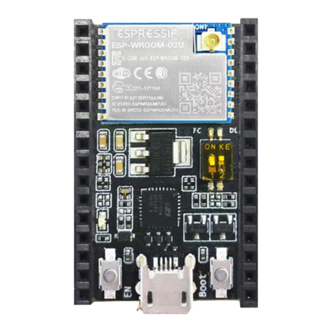
Espressif Systems
Espressif Systems ESP8266 SDK AT Instruction Set
Nuvoton
Nuvoton ISD61S00 ChipCorder Design guide
STMicrolectronics
STMicrolectronics ST7 Assembler Linker user manual
Texas Instruments
Texas Instruments Chipcon CC2420DK user manual

Texas Instruments
Texas Instruments TMS320F2837 D Series Workshop Guide and Lab Manual
CYPRES
CYPRES CY14NVSRAMKIT-001 user guide
Texas Instruments
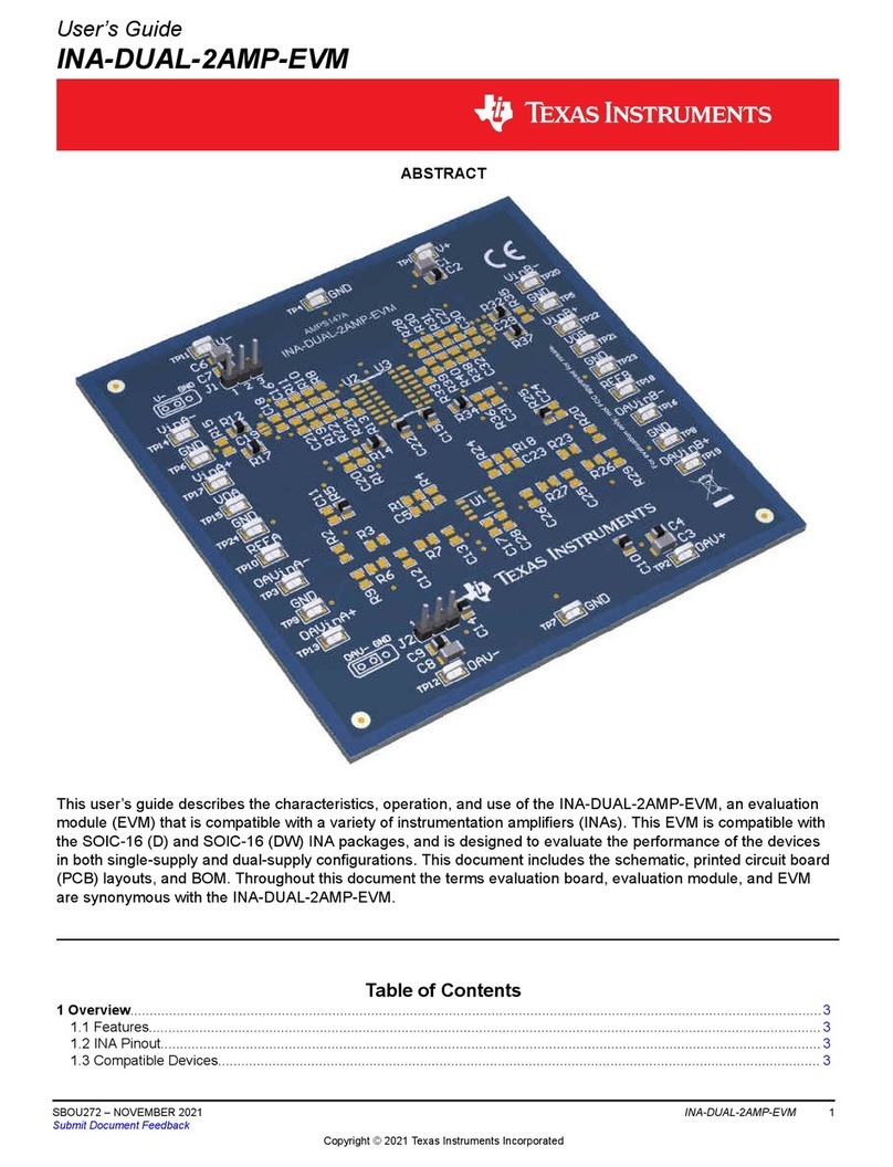
Texas Instruments INA-DUAL-2AMP-EVM user guide
Espressif Systems
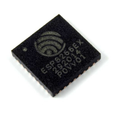
Espressif Systems ESP8266EX Programming guide
Abov
Abov AC33M8128L user manual
Laird
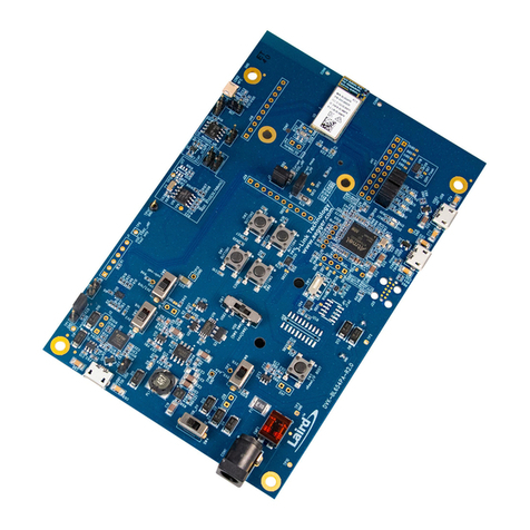
Laird BL654PA user guide
