Oki OKICOLOR 8 User manual

OKICOLOR 8
Color LED Page Printer
Maintenance Manual
1999.7.14 Rev. 1

41057610TH Rev. 1 2 /
PREFACE
This maintenance manual provides procedures and techniques for the troubleshooting, maintenance, and
repair of OKICOLOR 8.
This manual is written for maintenance personnel, but it should always be accompanied with the
OKICOLOR 8 User’s Manual for procedures for handling and operating the OKICOLOR 8.
For repairing each component of OKICOLOR 8, see the Troubleshooting manual.
[Notices]
The contents of this manual are subject to change without prior notice.
Although reasonable efforts have been taken in the preparation of this manual to assure its accuracy, this
manual may still contain some errors and omissions. OKI will not be liable for any damage caused or
alleged to be caused, by the customer or any other person using this maintenance manual to repair,
modify, or alter the OKICOLOR 8 in any manner.
[Warning]
Many parts of OKICOLOR 8 are very sensitive and can be easily damaged by improper
servicing. We strongly suggest that OKICOLOR 8 be serviced by OKI’s authorized technical service
engineers.

41057610TH Rev. 1 3 /
CONTENTS
1.SPECIFICATIONS............................................................................................6
1.1 Basic System Configuration.............................................................................................6
1.2 Printer Specifications.......................................................................................................7
1.3 Option Specifications.......................................................................................................8
1.4 Basic Specifications........................................................................................................9
2.OPERATION...................................................................................................12
2.1 Main Control Board (PCE PCB)....................................................................................13
2.2 Engine Control Board (PX4 PCB)..................................................................................16
2.3 Power/Units....................................................................................................................17
2.4 Mechanical Processes...................................................................................................18
2.4.1 Electrophotographic processing mechanism....................................................19
2.4.2 Paper running process.....................................................................................25
2.5 Sensors..........................................................................................................................34
2.5.1 Paper related sensors......................................................................................34
2.5.2 Other sensors...................................................................................................35
2.6 Correction of Color Deviation.........................................................................................36
2.7 Transfer Control according to Environmental Changes
(Room Temperatures and Relative Humidities).............................................................36
2.8 Form Jam Detection.......................................................................................................37
2.9 Cover Opening...............................................................................................................37
2.10Toner Low Detection......................................................................................................38
2.11Page Size Detection......................................................................................................39
2.12Power-on Processing.....................................................................................................40
2.12.1Self-diagnostic test...........................................................................................40
3.PARTS REPLACEMENT................................................................................41
3.1 Precautions for Parts Replacement...............................................................................41
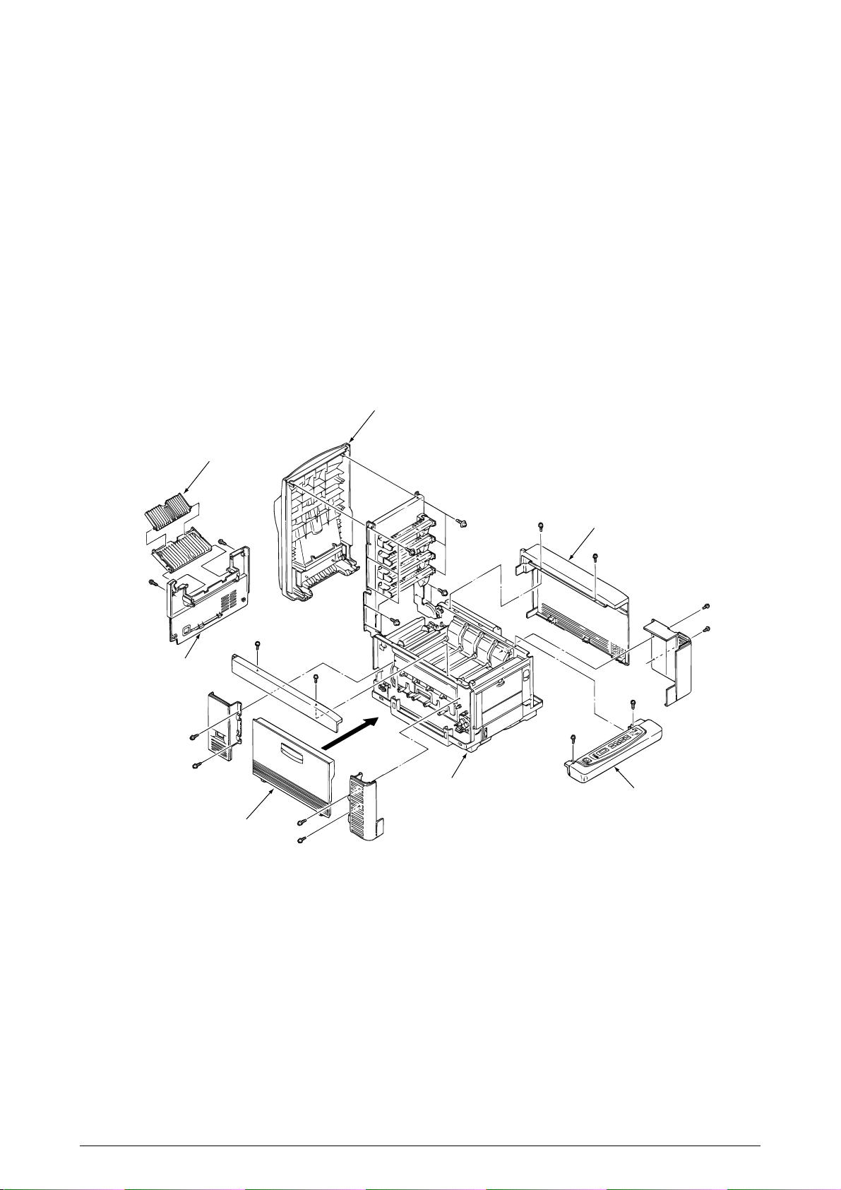
3.2 Parts Layout...................................................................................................................43
3.3 How to Change Parts.....................................................................................................47
3.3.1 Cover Assy Rear..............................................................................................48
3.3.2 Motor-Fan (80-25)............................................................................................49
3.3.3 Paper Eject Assy..............................................................................................50
3.3.4 Cover Assy Stacker, Guide Eject FD Assy.......................................................51
3.3.5 Frame Assy Upper............................................................................................52
3.3.6 Plate Support Assy...........................................................................................53
3.3.7 Limiter 2way (L), (R) / Plate Guide (L) , (R)......................................................54
3.3.8 Cover55
3.3.9 PCB Assy : PCE...............................................................................................56
3.3.10Motor Fan (CU).................................................................................................57
3.3.11PXF PCB/PX4 PCB..........................................................................................58
3.3.12Gear Heat Assy................................................................................................59
3.3.13Main Motor (A), (B) Assy..................................................................................60
3.3.14Gear One-way (Z30).........................................................................................61
3.3.15Motor Assy BT..................................................................................................62
3.3.16Power Supply Unit, Holder Inlet, Sheet Insulation............................................63
3.3.17Sensor Assy Box Toner....................................................................................64
3.3.18Square-shaped Connector...............................................................................65
3.3.19Hopping Motor..................................................................................................66
3.3.20Gear One-way..................................................................................................67
3.3.21Feeder Unit Front.............................................................................................68
3.3.22Manual Feed Hopper Assy...............................................................................69
3.3.23Guide Paper Input Assy....................................................................................70
3.3.24Two Lever Input Sensors, Lever 2nd Feed Sensor..........................................71
3.3.25Roller Registration, Roller Assy Hopping.........................................................72

41057610TH Rev. 1 4 /
3.3.26Roller Hopping..................................................................................................73
3.3.27PXU PCB/PXM PCB, Lever Resist Sensor......................................................74
3.3.28Paper End Lever...............................................................................................75
3.3.29PCO PCB (Operator Panel)..............................................................................76
3.3.30Holder Gear Toner Assy...................................................................................77
3.3.31Plate Latch Lever (FD), Spring Latch Lever (FD).............................................78
3.3.32Belt Cassette Assy...........................................................................................79
3.3.33High Voltage Power Supply Unit, Bracket HV (BT) Assy.................................80
3.3.34Eraser Bracket Assy, Eraser Bracket (KCM) Assy...........................................81
3.3.35Shaft Link..........................................................................................................82
3.3.36Contact (BL-R) Assy, Contact (CL-R) Assy......................................................83
3.3.37Contact (BL-L) Assy, Contact (CL-L) Assy.......................................................84
3.3.38Contact SB Assy...............................................................................................85
3.3.39PXC PCB..........................................................................................................86
3.3.40Heat Unit Assy..................................................................................................87
3.3.41Oil Roller Assy..................................................................................................88
3.3.42Lever Lock Heat (L)/(R), Guide Side Heat, Spring Lock...................................89
3.3.43PXL PCB..........................................................................................................90
3.3.44Heat Unit Guide Assy.......................................................................................91
3.3.45Holder LED Assy, LED Head............................................................................92
4.ADJUSTMENTS.............................................................................................93
4.1 Maintenance Modes and Their Functions......................................................................93
4.1.1 User maintenance mode..................................................................................93
4.1.2 System maintenance mode..............................................................................95
4.1.3 Engine maintenance mode...............................................................................97
4.2 Adjustments after Parts Replacement.........................................................................100
4.2.1 Confirm the LED head driving time.................................................................100
4.2.2 Color deviation correction...............................................................................102
5.PERIODIC MAINTENANCE.........................................................................105
5.1 Periodically Replaced Parts.........................................................................................105
5.2 Cleaning.......................................................................................................................105
5.3 Cleaning the LED Lens Array......................................................................................105
5.4 Cleaning the Pickup Roller...........................................................................................105
6.TROUBLESHOOTING PROCEDURES.......................................................106
6.1 Troubleshooting Tips...................................................................................................106
6.2 Points to Check before Correcting Image Problems....................................................106
6.3 Tips for Correcting Image Problems............................................................................106
6.4 Preparation for Troubleshooting..................................................................................107
6.5 Troubleshooting Flow...................................................................................................107
6.5.1 LCD status message/trouble list.....................................................................107
6.5.2 LCD message troubleshooting.......................................................................116
6.5.3 Image troubleshooting....................................................................................128
7.WIRING DIAGRAM......................................................................................145
7.1 Resistance Check........................................................................................................145
7.2 Program/Font ROM Location.......................................................................................149
8.Parts List......................................................................................................153

41057610TH Rev. 1 5 /
Appendix A CENTRONICS PARALLEL INTERFACE.....................................173
Appendix B HIGH CAPACITY SECOND PAPER FEEDER............................177
1. OUTLINE................................................................................................177
1.1Functions.............................................................................................................177
1.2External View and Component Names................................................................177
2. MECHANISM DESCRIPTION................................................................178
2.1General Mechanicsm...........................................................................................178
2.2Hopper Mechanism.............................................................................................179
3. PARTS REPLACEMENT.......................................................................180
3.1Precautions Concerning Parts Replacement.......................................................180
3.2Parts Layout........................................................................................................182
3.3Parts Replacement Methods...............................................................................183
3.3.1Idle rollers.............................................................................................184
3.3.2AOLT-PCB...........................................................................................185
3.3.3Hopping motor......................................................................................186
3.3.4Feed roller............................................................................................187
3.3.5Hopping roller.......................................................................................188
3.3.6Side frame (L) assy..............................................................................189
3.3.7Side frame (R) assy..............................................................................190
4. TROUBLESHOOTING...........................................................................191
4.1Precautions Prior to the Troubleshooting............................................................191
4.2Preparations for the Troubleshooting..................................................................191
4.3Troubleshooting Method......................................................................................192
4.3.1LCD Status Message List.....................................................................192
4.3.2Troubleshooting Flow...........................................................................193
5. CONNECTION DIAGRAM.....................................................................194
5.1Interconnection Diagram.....................................................................................194
5.2PCB Layout.........................................................................................................195
6. PARTS LIST..........................................................................................196

41057610TH Rev. 1 6 /
MMMM M MM M
LED head Discharging indicators
Centronics
interface Controller Junction board Pulse motors
Engine controller
Low-voltage
power unit
Fixing unit
High-voltage
power unit Second tray
Belt unit
<Sensors, switches, and thermistors>
Paper width sensor
Form size detector (4 bits)
Form end sensor
FF form end
FF home switch
Form feed sensor 1
Form feed sensor 2
Write sensor
Ejection sensor
Toner Low (Y.M.C.K)
EP Up/Down (Y.M.C.K)
Waste toner sensor
Resist Up/Down
Cover open switch (High-voltage
interlock switch)
Heater temperature thermistor
Backup temperature thermistor
Environment temperature sensor
Environment humidity sensor
Oil Roller switch
Fixing unit interlock switch
Waste toner box switch
Y-EP unit M-EP unit C-EP unit B-EP unit
PSIMM
x2
interface
SIMM
x4
interface
CEPM EPYEPK EPBELTHEATERREGISTFF
Operator panel
1. SPECIFICATIONS
1.1 Basic System Configuration
The basic system configuration of OKICOLOR 8 is illustrated in Figure 1.1.
Figure 1.1

41057610TH Rev. 1 7 /
1.2 Printer Specifications
This printer unit is composed with the following hardware.
•Electro-photographric processor
•Paper feeder
•Controller (CU part / PU Part)
•Operator panel
•Power board (High voltage part / PU part)
Figure 1-2 show the printer unit configuration.
Figure 1.2
Face-up Stacker Assy
Stacker Cover Assy
Rear Cover
Side Cover (L) Assy
Base Unit Operator Panel Assy
I/F Cover Assy

41057610TH Rev. 1 8 /
1.3 Option Specifications
Options available for OKICOLOR 8 are as follows.
(1) 2nd-Feeder
(2) RAM SIMM module (72 pin SIMM, 4MB/8MB/16MB/32MB)
* Make sure to use a set of 2 of the same volume size modules.

41057610TH Rev. 1 9 /
1.4 Basic Specifications
(1) Dimensions
Width: 18.8" (478mm) Length: 24.5" (622mm) Height: 15.6" (396mm)
(2) Weight
Approx. 48kg (106lbs)
(3) Form
Type: Ordinary paper (Hammermill 24lbs) and OHP (Only 3M CG3710)
Recommended paper (for color printing)
Color laser paper (20lb to 24lbs)
Note: The printout color tones are dependent upon the whiteness of the print
paper
Sizes: Letter, Legal (13"or 14"), Executive, A4, A5, B5, and A6 (1st tray and front feeder)
Reams:1st tray 20lbs to 28lbs
2nd tray 20lbs to 28lbs
Front feeder 20lbs to 53lbs (110lbs index)
(4) Printing speed
8 pages per minute (5 pages per minute: Card Stock, Labels & OHP/ 34lbs ~44lbs)
(5) Resolution
600 dots per inch x 600 dots per inch
(6) Input voltage
120VAC +5.5%, -15%
230VAC ±10%
(7) Power consumption
Peak: Typical operation
Idle: Power-save mode
(8) Frequency
50Hz or 60Hz +2%, -2%
(9) Noise
Operating: 54dB (without 2nd tray), 55dB (with 2nd tray)
Standby: 45dB
Power-saving: 43dB
(10)Consumables and service life
Toner cartridge: Approx. 3000 pages (5% duty) (each of C, M, Y, and K)
(Approx. 2000 sheets for the first)
Image drum: Up to 13,000 pages (5% duty, continuous) (each of C, M, Y, and K)
Waste Toner Box:Up to 25,000 Sheets
(under typical printout conditions: Single images of 5% density,
equivalent to printout using 14 toner cartridges)
Oil Roller Unit: Up to 10,000 sheets (Life defined in the number of actually printed
paper sheets)
(11)Periodically-replaced parts
Heat Unit Assy: 60,000 pages
Belt Cassette Assy:50,000 pages

41057610TH Rev. 1 10 /
(12)Temperatures and relative humidities
Temperature Temperature conditions
Temperature (in _F) Temperature (in _C) Remarks
60.8 to 89.6
50 to 109.4
33 to 109.4
-20 to 122
-20 to 122
16 to 32
10 to 43
0.6 to 43
-29 to 50
-29 to 50
Operating
Non-operating
Storage (1 year max.)
Delivery (1 month max.)
17_C to 27_C (for assurance
of full-color printout quality)
Power off
with drum and toner
without drum and toner and
Belt Cassette Assy
with drum and toner
(13)Printer life
3,000,000 (A4) pages or 5 years
Humidity Humidity condition
Relative humidity (%)Wet-bulb temperature Remarks
20 to 80
10 to 90
10 to 90
10 to 90
25
26.8
35
40
Operating
Non-operating
Storage
Delivery
50% to 70% (for assurance of
full-color printout quality)
Power off
for the packed unit only

41057610TH Rev. 1 11 /
This page intentionally left blank

41057610TH Rev. 1 12 /
2. OPERATION
OKICOLOR 8 is a tandem color electrophotographic page printer, using 4992-LED technologies,
OPC, dry single-component non-magnetic developing, roller transfer, heat-
compression fixing and so on. The printing method used is a Black Writing method which applies
light beams to printout areas.
Figure 2.1 shows the functional block diagram of OKICOLOR 8.
Figure 2.1
AC-IN AC switch
Crimp-style terminal
PXLboard
PXL
Ejection sensor
LED head:CMYK
Discharging lamp:CMYK
Heat roller
thermistor
Backup roller
thermistor
Heater unit
SUMi card x 4 PD6 board
C600 14P
CPOW 12P M600 14P
MPOW 12P Y600 14P
YPOW 12P K600 14P
KPOW 12P
HEAD1 13P HEAD2 14P HEADPOW 12P HEAD3 15P
FF form
sensor Toner sensor x 4
ID sensor x 4
Low-voltage power supply
6P
6P'
JST3P
FAN 1
FAN 2
3P
Oil PAD MSW
FF
motor
Paper supply sensor board
FF Pos MSW
PXM board
40095001YU
REG.POS
sensor
Resist
motor C-IDU
motor M-IDU
motor Y-IDU
motor K-IDU
motor Belt
motor Heat
motor
PXF board
JODEN 8P
FSENS 8P
TONER
14P
PXFIF 30P
OPTION 7P
PENDTNR 6P
PX4 board
2nd tray
(option) Form end
sensor Waste toner
sensor
YIDREG
8P MCKID
12P HETBELT
8P HEAD3
15P HEAD2
14P HEAD1
13P HEADPOW
12P
FF 12P
PXFIF 30P HVOLT16P COVOPN 2P PSIZE 6P
High-voltage power supply PXC board Form size detector
Cover open
MSW
PCE
Operator
panel
PCO
board
CM
6P
PU 40P
72PX2
PS SIMM 72PX4
D-RAM SIMM 64P
OKI HSP 36P
Parallel
CUIF 40P
POWER 30P
THE.RM 6P
RSENS 7P
Interlock switch
UPDOWN
12P

41057610TH Rev. 1 13 /
2.1 Main Control Board (PCE PCB)
The control board consists of a CPU (200MHz) block, a memory control LSI block, an
interface control LSI block, a DRAM block, an EEPROM block, a mask ROM block, and an interface
block. Figure 2.2 shows the functional block diagram of the main control board (PCE PCB).
Figure 2.2
2nd cache
controller
Control
Control
MPU Memory controller ROM, Flash Max 32M
D-RAM Max 144M
EE-PROM
74LVC161284 Bi-Centro
OKI HSP
Host I/F(Not installed)
(TE6135 (6137), 16550, 53C80)
Engine
Interface controller Operator
panel
OSC
Reset circuit
DIPSW
SysAD
SysCmd
Control
NMI
INTO
ExtReg
INT1
Reset
ColdReset
VCCOK
ModeIn
ModeClock
MasterClock
SysAD
SysCmd
Control
SysAD
µ
PD30500
S2-200
64
9
5
22
64
11
11
64
25
8
4
4
9
4
1
1
1
8
5
4
16
18
12
10
1
1
1
1
1
1
1
1
1
1
2
1
64
9
5
1
1
CLK
RSTIN
M
Reset
uPU66044
GN-014-LMU
SysAD
SysCmd
Control
ExtReq
INT
SysAD
SysCmd
Control
NMI
INT
CLK
RST
PU I/F
OPI/F
A
D
Control
A
D
Control
WDATA
FSYNC
Control
WDATA
ESYNC
Control
EEPD
EEPCLK
EEPCS0
DI
CLK DO
CS
PD
PCO
PCI
D
A
C
ColdReset
VCCOK
ModeIn
ModeClk
uPD94704
S1-001-F6

41057610TH Rev. 1 14 /
(1) CPU
The CPU is a 64-bit RISC architecture processor (provided by NEC). It inputs a frequency
of 50MHz and runs at 200MHz. It transfers data to and from memory at 50MHz.
(2) MASK ROM
The Mask ROM block consists of four 16Mbit (1M x 16bits) chips and its total size is 8M bytes.
The chips are mounted on the PCE-PCB by means of IC sockets and store programs and
character fonts.
(3) DRAM
The DRAM block consists of eight 16Mbit (1M x 16bits) chips and its total size is 16M bytes.
The chips are mounted on the PCE-PCB and can be expanded up to 144M bytes by adding
the 32M byte SIMMs to the SIMM slots on the PCE-PCB.
(4) EEPROM
The EEPROM block consists of 16K-bit chips mounted on a board by means of IC sockets
and stores the following:
-Menu data
-Counter values
-Adjustment values
(5) Flash ROM
The Flash ROM block consists of four 4M bit (256K x 16bits) chips and its total size is 2M
bytes. The chips are mounted on the PCE-PCB and are used for storing fonts, macro and
demo pages.
(6) Memory control LSI
This block mainly consists of memory control, CPU control, compression and decompres-
sion, and video interface functions.
(7) Interface control LSI
This block mainly consists of PU interface control, operator panel interface control, EEPROM
control, parallel interface control, and HSP control functions.
(8) Host interface
This printer has the following interfaces to the host.
•Centronics bidirectional parallel interface
•Network interface (Option)
The single effective interface or the automatic interface select mode can be selected using
the menu. If the busy state of the printer continues for a long time period, the buffer near-full
control releases the busy status at constant intervals even if the host side is busy so as not
to cause interface time-out at the host side.
(a)Centronics bidirectional parallel interface
This is an interface conforming to IEEE-1284 and provides either unidirectional and
bidirectional communications according to each of the following communication modes.
•Compatibility mode
Unidirectional communications from the host to the printer.
•Nibble mode
This mode transfers 4-bit wide data from the printer to the host. In this mode, each
bit of 1-byte data is transmits in the form of two nibbles using ERROR, BUSY, FAULT,
and SELECT signal leads. This mode can provide bidirectional operation in
combination with the compatibility mode.

41057610TH Rev. 1 15 /
• Basic specificaton
- Type: 72 pins SIMM (32 bits buss width)
- Access time: 60ns, 70ns, 80ns
- Capacity: 4, 8, 16 or 32MB
- Parity: None
(9) 2nd Cache and 2nd Cache Controller
This printer has the 2nd Cache unit which type is Write Through Cache and size is 512 KByte.
There are any difference between the instruction and data. All of the CPU read/write access
are cached to same 2nd cache memory.
(10) RAM module
• Pin layout
• ECP mode
This mode provides the asynchronous bidirectional interface and transmits and
receives 1-byte data using eight data signal leads under semi-duplex control by the
host.
When the power is turned on, the compatibility mode is automatically selected. The
change to another mode from the compatibility mode is made through negotiation.
(When the BI DIRECTION is set to ENABLE in the menu, this change can be performed.)
(For the electrical/physical characteristics of this interface, see APPENDIX B)
(b) Network interface (Option)
Network interface card uses the power line only.
Figure 2.3
Printer
Control board LAN
expansion board
interface
Power Line only Network, etc.
1363772

41057610TH Rev. 1 16 /
Figure 2.4
The engine control block (PU) is controlled by the engine control board (PX4 PCB) which consists
of a CPU (MSM65524), general purpose LSI chips, EPROM, EEPROM, pulse motor drivers, and
video memory. (See Figure 2.4.)
(1) CPU
This is an 8-bit CPU (OKI MSM65524) containing the AD converter and controls the whole
system.
(2) General-purpose LSI
This LSI (MB87D113PFV) is provided in the printer engine control block and has controller-
engine video interface, LED interface, motor control, sensor input, video memory control,
main scanning color correction, skew correction, high-voltage power control, and OST-EX2
functions.
2.2 Engine Control Board (PX4 PCB)
CHEAD I/F (3.3V)
M HEAD I/F (3.3V)
YHEAD I/F (3.3V)
B HEAD I/F (3.3V)
MT DRIVER
MTD2005F
MT DRIVER
MTD2005F
MT DRIVER
MTD2005F
PULSE MOTOR x 8
LSI
MB87D
113PFV
ANALOG INPUT
(Heater temperatures and environment humidity and temperature)
HIGH-VOLTAGE POWER SUPPLY
SERIAL INTERFACE (2 channels)
GENERAL INPUT PORTGENERAL OUTPUT PORT
RESET
OSC 28MHz
VIDEO MEM
HM658512
VIDEO I/F
CPU BUS
EEPROM
NM93C66N-NW ROM
27512
CPU
MSM65524
(containing AD converter)
INT

41057610TH Rev. 1 17 /
Output voltage Use
+3.3 V CU Unit CPU, LED HEAD
+5 V Logic circuit supply voltage
+32 V Motor and fan drive voltage and source voltage for high-voltage supply, discharge lamp
+12 V HSP, OP Amp, high voltage power supply
–12 V HSP
Output Voltage Use Remarks
CH -1.35 KV
±
50V Voltage applied to charging roller
DB Normal paper Voltage applied to developing roller
Y. M. C : -250V/+300V, -232V/+300V(First paper. Y only)
K : -275V/+300V
Transparency
Y. M. C. : -200V/+300V, K. : -250V/+300V
SB Y. M. C.K : -650V/0V Voltage applied to toner supply roller
TR 0 to 4 KV Voltage applied to transfer roller Variable
FIX 0 to 2.5 KV Voltage applied to transfer roller Variable
(2) High voltage power supply unit
This circuit generates the following voltages necessary for electro-photographic processing
from +32 V in accordance with the control sequence from the control board. When cover open
state is detected, +32 V supply is automatically interrupted to stop the supply of all the high-
voltage outputs.
2.3 Power/Units
The power supply unit comprises of the low voltage power supply unit which consists of an AC filter
circuit, low voltage power supply circuit and heater driver circuit, and the high voltage power supply
unit.
(1) Low voltage power supply unit
This circuit generates the following voltages.
(3) EPROM
This EPROM (27C512-150) has a storage capacity of 512K bits and stores programs for the
PU block.
(4) EEPROM
This EEPROM (NM93C66N-NW) having a storage capacity of 4K bits is mounted on the
board by means of IC socket and stores adjustment values etc.
(5) Pulse motor drivers
These drivers (MTD2005F) drive eight pulse motors for moving up and down the EP and
transferring medium.
(6) Video memory
This SRAM receives print data through video interface and stores it.

41057610TH Rev. 1 18 /
2.4 Mechanical Processes
Figure 2.5 shows the mechanical processes of OKICOLOR 8.
Figure 2.5
Paper
ejection
roller
Paper
ejection
(Face down)
Power
supply
Charging
roller
Cleaning
blade
Paper
path
selection
Heat roller
Ejection
roller Fixing
Backup roller
Control signal
LED head
Developing
roller
Power
supply
Toner
cartridge
Transfer
roller
Paper
resist
Resist
roller 1
Paper
feed
Hopping
roller
Power
supply Resist
roller 2
Paper ejection Fixing Cleaning Transferring Paper pickup Paper conveying Paper hopping
Movement of
paper
Rotation of
OPC drum
Transferring
Charging
Exposure
Developing
Cleaning
Paper ejection
sensor Form feed sensor 1
Paper
ejection
(Face up)
Form feed sensor 2
Front
feeder
Paper
cassette
Paper
resist
Paper
pickup
(FF, 1ST, 2ND)
Write sensor
x 4
Y M C K

41057610TH Rev. 1 19 /
2.4.1 Electrophotographic processing mechanism
(1) Electrophotographic processes
Each process of the electrophotographic processing mechanism is outlined below.
1Paper pickup
Thisprocess causes theroller togive a DCvoltage tothe paper tohave anegative charge.
With this negative charge, the paper is electrostatically attracted to the roller.
2Charging
Thisprocess gives aDC voltageto theCH roller sothat theOPC drummay have auniform
negative charge on its surface.
3Exposure
This process causes the LED head to apply light beams according to image signals to the
negatively-charged surface of the OPC drum. The negative charge on the illuminated
surface of the OPC drum is reduced according to magnitudes of the light beams.
Thus, a latent image is formed on the surface of the OPC drum according to the resulting
surface potentials.
4Developing and recovery of excessive toner
This process applies negatively-charged toner to the surface of the OPC drum. The toner
is electrostatically attracted to the latent image to form a visible image on the surface of
the OPC drum. Simultaneously, this process electrostatically transfers excessive toner
from the OPC drum to the developing roller.
5Transferring
This process fits paper to the surface of the OPC drum, applies positive charge (opposite
to the charge of the toner) to the back side of the paper from the transfer roller. The toner
image is transferred to the paper.
6Cleaning
Cleaning blade scrapes off the remaining toner from the OPC drum which has been used
to transfer.
7Fixing
This process fixes the toner image on the paper by pressing and fusing the image.
Other manuals for OKICOLOR 8
3
Table of contents
Other Oki Printer manuals

Oki
Oki ML620 User manual

Oki
Oki 390/391 User manual

Oki
Oki ES1220n User manual

Oki
Oki proColor pro900DP User manual

Oki
Oki C910 Assembly Instructions

Oki
Oki C9650hn User manual

Oki
Oki C9500 Series User manual

Oki
Oki C911dn Assembly instructions

Oki
Oki B6500 Series User manual

Oki
Oki C5200n Series User manual