Osram ams TSL2521 User manual

Product
Document
Published by
ams OSRAM Group

Document Feedback
TSL2521 ALS/Flicker
Content Guide
Application Note •PUBLIC
AN001042 •v1-01 • 2022-Jan-27
23 │2
Content Guide
1Introduction ................................... 3
2TSL2521 ALS and Flicker
Settings.......................................... 4
2.1 ALS Channels/Modulators............................4
2.2 Sequencer....................................................5
2.3 Residual Measurement ................................5
2.4 ALS and Flicker Timing................................9
2.5 ALS/Flicker Gain and AGC.........................11
2.6 Wait Time ...................................................12
3ALS Result Data Format ............. 13
3.1 Internal Data Format ..................................13
3.2 16-Bit Data Full Count Results in ALS_DATA
Registers ....................................................14
3.3 20-Bit Data Result in ALS_DATA Registers
Including 4-Bit Residuals............................14
3.4 24-Bit ALS Result Data Transferred Via
FIFO............................................................16
3.5 Saturation and Maximum Value of ALS
Result..........................................................16
4Flicker Result Data Format .........19
4.1 Internal Flicker Data Format.......................19
4.2 Flicker Data Reduction Options..................19
4.3 Flicker Data Transfer Via FIFO...................20
5Revision Information...................22
6Legal Information.........................23

Document Feedback
TSL2521 ALS/Flicker
Introduction
Application Note •PUBLIC
AN001042 •v1-01 • 2022-Jan-27
23 │3
1 Introduction
TSL2521 offers new ALS and Flicker measurement features on a very small space of 2.0 mm x
1.0 mm x 0.5 mm compared to legacy devices. ALS and flicker are running on the same time base,
the FIFO is larger, it has some data compression features, and measurements can be planned in
sequences with individual settings. Additionally, a new residual measurement feature offers higher
resolution at lower gain.
These new features –especially regarding timing and sequences –require registers different than on
legacy ALS devices like TCS3707 –consequently the registers have now different names.
This document explains the settings for ALS measurements compared to legacy ALS devices, e.g. the
TCS3707 and shows the new relation between ALS and Flicker measurements.

Document Feedback
TSL2521 ALS/Flicker
TSL2521 ALS and Flicker Settings
Application Note •PUBLIC
AN001042 •v1-01 • 2022-Jan-27
23 │4
2 TSL2521 ALS and Flicker Settings
2.1 ALS Channels/Modulators
The datasheets of ALS legacy devices used to name the measurement channels after their filters, e.g.
the Clear channel, Red channel, Blue Channel and so on. It was possible on devices like TCS3707 to
change the Diode-to-channel connection via a multiplexer, but this was not easy during measurements
and therefore not often used.
The TSL2521 has only two ALS channels but it is very easy to change the connection between the
individual diodes –no matter which filter is on this diode –and the ALS engine. Consequently, channel
related registers are not named after the filter characteristic of the diodes –like Clear (C) and Infrared
(IR) –but after the two available ALS modulators: modulator 0 and modulator 1.
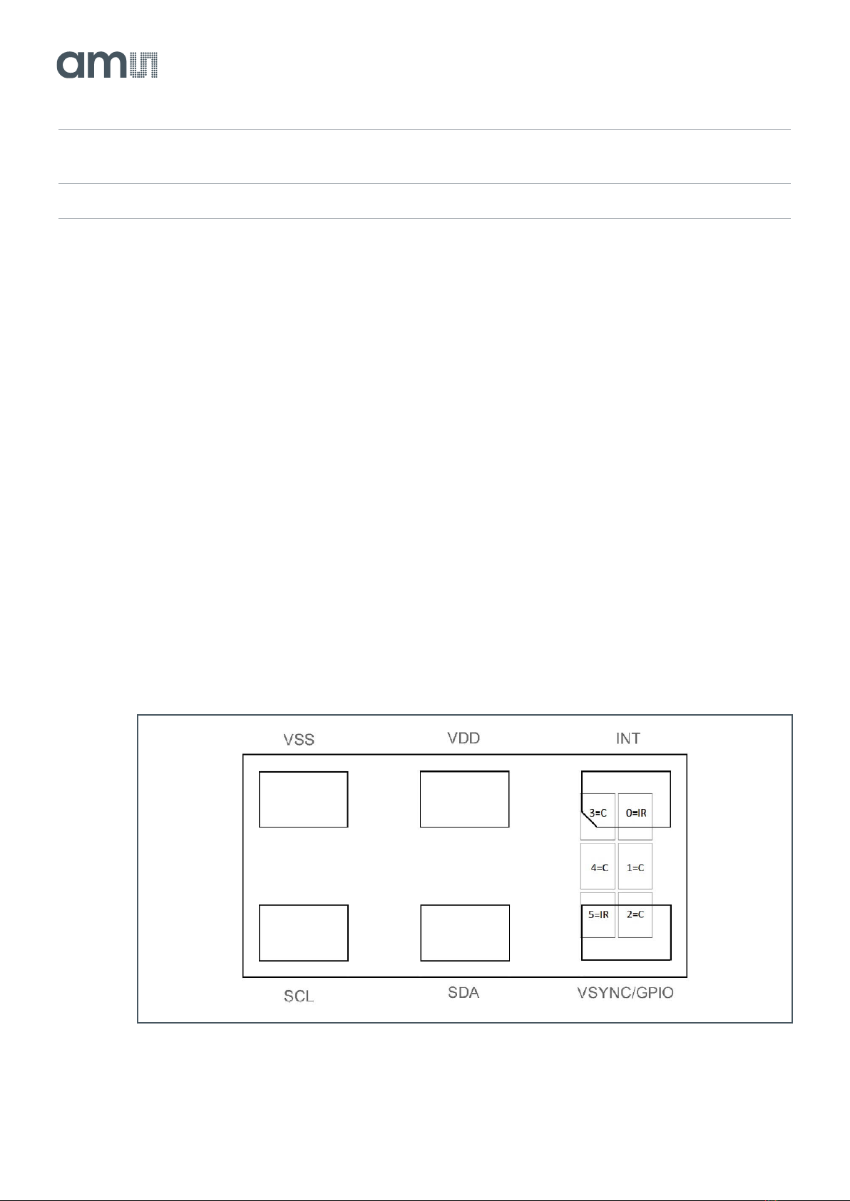
Figure 1 shows the number and filter type of the six available photodiodes on TSL2521. The
photodiode numbers are used to connect the photodiodes to the modulators in the SMUX registers
MEAS_SEQR_STEP0_MOD_PHDX_SMUX_L up to MEAS_SEQR_STEP3_MOD_PHDX_SMUX_H.
The default setting has to be changed since it refers to a different filter layout: modulator 0 should be
connected to the four Clear diodes 1, 2, 3, and 4; modulator 1 should be connected to the two IR
diodes 0 and 5. There is no separate channel/modulator for the flicker measurements, every
modulator can be used for both ALS and Flicker measurements at the same time. On TSL2521 flicker
measurements should be done preferred on modulator 0 with the Clear diodes.
The GUI and the drivers provided by ams OSRAM have both mentioned changes implemented.
Figure 1:
Location, Filter Type, and Number of Photodiodes of TSL2521 (top view)

Document Feedback
TSL2521 ALS/Flicker
TSL2521 ALS and Flicker Settings
Application Note •PUBLIC
AN001042 •v1-01 • 2022-Jan-27
23 │5
Information
In application cases with high transmissivity glass direct sunlight could cause saturation even at
gain setting of 0.5x especially on modulator 0 connected to the Clear diodes. This can be avoided
by connecting less than 4 of the Clear diodes to modulator 0 in the SMUX registers of the
sequencer.
2.2 Sequencer
TSL2521 has a programmable sequencer for ALS and Flicker measurements built in. There are 4
sequencer steps –step 0 to step 3 –available, but not all need to be used.
In ALS legacy devices like TCS3707 there is no comparable sequencer available, so that would be
like using only step 0 of the TSL2521. For a simple two channel ALS/Flicker measurement one step
might be enough, therefore the default settings of the TSL2521 only use step 0.
For more flexibility, some settings can be chosen for each sequencer step individually, most of them
organized in a 4-bit pattern - each bit of the pattern represents a single step. ALS needs to be enabled
in such a pattern in measurement_sequencer_als_pattern in register MEAS_SEQR_ALS_FD_1 for
both modulators, by default ALS with both modulators is enabled for step 0 only.
Flicker measurement can be enabled for each modulator individually, so there are two pattern fields,
measurement_sequencer_mod0_fd_pattern and measurement_sequencer_mod1_fd_pattern, both in
register MEAS_SEQR_FD_0.
The time a sequencer step lasts is defined by the ALS integration time, the Flicker measurement time,
or the Wait time –whatever is activated and lasts longer. The same is valid for the whole sequencer
cycle if only step 0 is performed.
If in a step there is neither ALS nor Flicker nor Wait time enabled by using the respective patterns then
this step will be omitted.
2.3 Residual Measurement
Residual measurement is a new feature on TSL2521 that enables to measure Sub-LSBs on ALS and
flicker data at the end of the integration time. Residuals represent fractions of full counts: the
integrating ADC –the ALS modulator –like on legacy devices normally counts only a 1 when the
capacitor charged by the photocurrent reached a certain voltage. When the integration time is over,
normally the remaining charge that did not reach this voltage is discharged. The idea of the Residual
measurement is that this remaining charge is measured to get fractions of full counts.

Document Feedback
TSL2521 ALS/Flicker
TSL2521 ALS and Flicker Settings
Application Note •PUBLIC
AN001042 •v1-01 • 2022-Jan-27
23 │6
Since the Residual measurement is done with a resolution of max. 4 bits on this device that results in
4 extra resolution bits almost for free. That way it is possible to use lower gains that have a better
linearity than higher gains, because the Residual bits provide additional resolution on LSB side.
Nevertheless, that has a limit too, so the Residual measurement resolution is reduced at higher gains
–that is why residual measurement is mainly suited to increase the resolution at medium and lower
gains.
There are two different gain tables, the default one reduces the evaluated number of residual bits
starting at gain 128x upwards by 1 for each gain step. The second gain table is valid up to gain 256x
and always uses 4 bits for residuals. It is recommended to use the second gain table and restrict the
maximum gain to 256x. Adding the 4 bits Residual resolution results in an effective gain of 4096x in
this case –but at the gain non-linearity of 256x, which is rather low.
In order to use the second gain table mod_gain_select has to be set to 3 before starting the
measurement, this field can be found in register MOD_GAIN_H as shown in Figure 2. The field
measurement_sequencer_max_mod_gain has to be set to 9 in register CFG8 to restrict the modulator
gain to 256x.
Figure 2:
MOD_GAIN_H
Addr: 0xED
MOD_GAIN_H
Bit
Bit Name
Default
Access
Bit Description
7:6
Reserved
0
5:4
MOD_GAIN_SELECT
0
RW
One bit for each channel to
select second gain table.
This register has to be
written before enabling the
sequencer!
3:0
Reserved
0
Figure 3 shows the Number of Residual bits for the gain steps of the two gain tables. If less than 4
Residual bits are used the non-used bits starting from LSB side are set to 0. This leads to higher
minimum step sizes of the ALS or Flicker sample results as well.
Figure 3:
Number of Residual Bits Depending on Gain Table Chosen by mod_gain_select
Mod_gainx [gain]
Number of Residual Bits for
mod_gain_select = 0
Number of Residual Bits for
mod_gain_select = 1
0 [0.5x] –8 [128x]
4
4
9 [256x]
3
4
10 [512x]
2
Reserved
11 [1024x]
1
Reserved

Document Feedback
TSL2521 ALS/Flicker
TSL2521 ALS and Flicker Settings
Application Note •PUBLIC
AN001042 •v1-01 • 2022-Jan-27
23 │7
Mod_gainx [gain]
Number of Residual Bits for
mod_gain_select = 0
Number of Residual Bits for
mod_gain_select = 1
12 [2048x]
0
Reserved
13 [4096x]
0
Reserved
The additional Residual resolution can be expressed either as decimal places after the full integration
counts or –as internally done - with additional bits on LSB side to avoid a floating-point format. Since
there are 4 bits added on the LSB side for Residuals –no matter if they are measured or not –the way
to get back to the same number space comparable to legacy devices is to divide the results by 16, in
this case the decimal places show the residual amount.
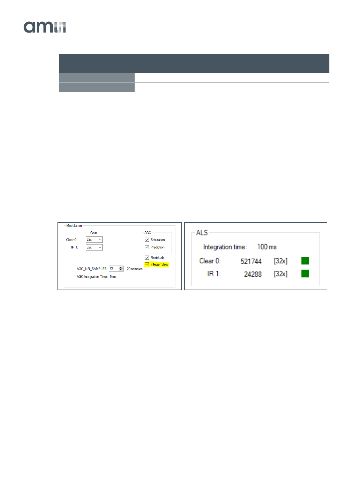
The GUI provided by ams OSRAM can show both methods, Figure 4 with the “Integer view box”
checked shows the internal integer view with 4-bit Residuals on LSB side like in Figure 5.
Figure 4:
TSL2521 GUI Configuration Tab With
Checked “Integer View” Box
Figure 5:
Internal Integer View With 4-Bit Residuals On
LSB Side
In contrast, “Integer View” box unchecked like in Figure 6 does the mentioned division by 16 to show
full counts and Residuals as fractions separated by the decimal point like in Figure 7, that way it can
be compared to the value of legacy devices e.g. for dark count measurements.

Document Feedback
TSL2521 ALS/Flicker
TSL2521 ALS and Flicker Settings
Application Note •PUBLIC
AN001042 •v1-01 • 2022-Jan-27
23 │8
Figure 6:
TSL2521 GUI Configuration Tab With
Unchecked “Integer View” Box
Figure 7:
Residuals Expressed as Fractions of Full
Counts
In order to activate the Residual measurement it needs to be enabled per step in
measurement_sequencer_mod0_residual_enable_pattern for modulator 0 and in
measurement_sequencer_mod1_residual_enable_pattern for modulator 1, both fields are in register
MEAS_SEQR_RESIDUAL_0.
One difference is that in case of enabled Residual measurement the last sampling time is reduced by
the Residual measurement time. This reduces the ALS integration time accordingly but only by a very
small amount and in case of no flicker measurement during the same step most times it can be
neglected as shown in Equation 1.
Equation 1:
In case of flicker measurements within the same step after each flicker sample measurement one
residual measurement is done. This reduces the whole ALS integration time more significantly as
shown in Equation 2. This needs to be considered when preparing or using a lux equation.
Equation 2:
Information
It is recommended to place ALS measurement and Flicker measurement into separate steps of the
sequencer in order to avoid noticeable influence of Residual measurement time onto the ALS
integration time. This is what the GUI and the drivers provided by ams OSRAM do as well.

Document Feedback
TSL2521 ALS/Flicker
TSL2521 ALS and Flicker Settings
Application Note •PUBLIC
AN001042 •v1-01 • 2022-Jan-27
23 │9
2.4 ALS and Flicker Timing
For ALS measurements one of the most important parameters is the ALS integration time. On legacy
devices like the TCS3707 that was the product of the modulator clock period at e.g. 2.78 µs, the value
in the ASTEP register (+1) and the value in the ATIME register (+1) as shown in Equation 3.
Equation 3:
On TSL2521, it is almost the same but the modulator clock changed to 1.3889 µs and the register/bit
field names are different as Equation 4 shows.
Equation 4:
On TSL2521, the first term –the modulator clock multiplied by sample_time –is the base sampling
time both for flicker measurements and for ALS measurements. If Flicker measurement is activated for
a modulator within the active sequencer step, every value at the end of the sampling time is pushed to
the FIFO –as often as set in fd_nr_samples in registers FD_NR_SAMPLES0 and
FD_NR_SAMPLES1 - and increases at the same time the ALS result –as often as set in
als_nr_samples in registers ALS_NR_SAMPLES0 and ALS_NR_SAMPLES1.
Therefore, the Flicker sampling frequency is the reciprocal of the sampling time set with register
SAMPLE_TIME, as shown in Equation 5.
Equation 5:
The whole flicker measurement time is defined by the mentioned sampling time and the register
FD_NR_SAMPLES, see Equation 6.
Equation 6:
Note that there is only one new ALS result after the ALS integration time for each modulator 0 and
modulator 1 since all single sample values are summed up. In contrast, there are fd_nr_samples
flicker results per chosen modulator in the FIFO after the Flicker measurement time of one step. If that
number of flicker results is more than the FIFO can handle –256 values with 16-bit width are normally
possible –the FIFO needs to be read out during the flicker measurement time to prevent a FIFO
overflow. Figure 8 and Figure 9 show the relation between ALS and flicker measurement within the
same step 0 of the sequencer with the chosen settings.

Document Feedback
TSL2521 ALS/Flicker
TSL2521 ALS and Flicker Settings
Application Note •PUBLIC
AN001042 •v1-01 • 2022-Jan-27
23 │10
Figure 8:
Step 0 of TSL2521 Sequencer with ALS and Flicker Measurement Activated
Figure 9:
Example Specification and Proposed Settings
Item
Value [dec.]
Customer Example Specification:
- Update interval
< 0.5 s
- ALS integraton time
50 ms
- Max. flicker frequency
2 kHz
- FFT bin size
10 Hz
Proposal:
- Sample time
125 µs
- Sample frequency
8 kHz
- FFT size
1024
Settings for Proposal:
- sample_time
89
- als_nr_samples
399
- fd_nr_samples
1023
400
4
1
2
3
ALS integration time
... Pause
4
1
2
3
...
1024
sample time Flicker measurement time
ALS Result
FIFO used for Ficker data

Document Feedback
TSL2521 ALS/Flicker
TSL2521 ALS and Flicker Settings
Application Note •PUBLIC
AN001042 •v1-01 • 2022-Jan-27
23 │11
2.5 ALS/Flicker Gain and AGC
Another fundamental parameter for ALS measurement is the ALS gain setting. For ALS legacy
devices like TCS3707 there was a single AGAIN value. For TSL2521, the gain is set per modulator
and even for every sequence individually. The gain for both modulator 0 and modulator 1 for step 0
can be set in register MEAS_SEQR_STEP0_MOD_GAINX_L. The modulator gain can range from
0.5x to 4096x and is limited in register CFG8 by the field measurement_sequencer_max_mod_gain for
all modulators and sequencer steps. Please note that in case of enabled Automatic Gain Control
(AGC) the modulator gain registers are changed according to the last measurement.
The gain used for the current result set in the ALS_DATA registers can be read from the
ALS_STATUS2 register using the bit fields als_data0_gain_status and als_data1_gain_status. This
gain information is important for the lux equation, since the AGC –if enabled –might have changed
the originally set modulator gain.
There are two Automatic Gain Control (AGC) methods implemented. The legacy one is the saturation
AGC that reduces the gain in case of modulator saturation and repeats the measurement until there is
no saturated result. This method is easy and –as long as the dynamic range allows it –always leads
to a useful result but can take longer time and the time delay caused by this procedure is not
deterministic.
The saturation AGC can be enabled in field measurement_sequencer_agc_asat_pattern in register
MEAS_SEQR_STEP1_MOD_PHDX_SMUX_H individually for each sequencer step. This setting is
valid for both modulators.
The second one is the predict AGC, that defines the gain for the next measurement by doing a
measurement with reduced gain. The gain reduction can be set in register CFG8 in the field
measurement_mod_gain_reduction; by default it reduces the gain by 4 steps. The advantage of the
predict AGC is a shorter and deterministic measurement time, but in case of abrupt changes it can
lead to a saturated result that needs to be dropped after checking the saturation signals.
The predict AGC can be enabled in the field measurement_sequencer_agc_predict_pattern in register
MEAS_SEQR_STEP2_MOD_PHDX_SMUX_H individually for each sequencer step. This setting is
valid for both modulators.
The AGC measurement is done by adding an additional ALS sequence round before the actual
measurement sequence. Both AGC methods do not need to use the same ALS integration time since
AGC has its own dedicated agc_nr_samples fields in registers AGC_NR_SAMPLE[7:0] and
AGC_NR_SAMPLES[10:8], sample_time is the same as for ALS/Flicker. That can help to reduce the
whole ALS measurement time by using a shorter integration time for the AGC measurement. Both
AGC methods can be used at the same time, in this case the predict AGC firstly sets the gain, but if
still analog saturation happens the saturation AGC repeats the measurement with reduced gain.
Please note that due to the saturation AGC method the ALS measurement time is not deterministic in
this case too.
How often AGC is performed is defined with mod_calib_nth_iteration in register MOD_CALIB_CFG0.
Additionally, the ACG needs to be linked to mod_calib_nth_iteration by setting the bit

Document Feedback
TSL2521 ALS/Flicker
TSL2521 ALS and Flicker Settings
Application Note •PUBLIC
AN001042 •v1-01 • 2022-Jan-27
23 │12
mod_calib_nth_iteration_agc_enable in register MOD_CALIB_CFG2. Please note that this bit is not
enabled by default but has to be enabled to use one or both of the AGC methods.
Information
The same mode_calib_nth_iteration setting is used for the Autozero as well. Since the ALS
Autozero procedure can take a longer time it might be necessary to disable the bit
mod_calib_nth_iteration_az_enable in register MOD_CALIB_CFG2 after the first measurement. For
this purpose a single measurement can be done after startup either by setting
mode_calib_nth_iteration to 1 and setting the bit stop_after_nth_iteration in register MEAS_MODE0
or just by stopping the measurement after getting the first result. After that Autozero can be disabled
by clearing bit mod_calib_nth_iteration_az_enable.
2.6 Wait Time
Related to ALS measurement on legacy ALS devices like TCS3707 was the Wait time that defined the
sample rate of the ALS measurement –and therefore had to be higher than the set ALS integration
time. The way to activate this WTIME was to set the enable Bit WEN in the ENABLE register.
WTIME is present on TSL2521 as well, but there is no WEN necessary anymore. Instead, there is the
additional bit field mod_trigger_timing in register TRIGGER_MODE that either switches off the Wait
time or defines the time base multiplicator for WTIME.
Additionally, the Wait time needs to be activated for each sequencer step individually in bit field
measurement_sequencer_wait_pattern in register MEAS_SEQR_RESIDUAL_1_AND_WAIT.
As for all sequencer pattern registers on TSL2521 the default value is the right one if only sequence
step 0 is used.
Information
Please note that on TSL2521 the Wait time needs to be higher than both the ALS integration time
and the Flicker measurement time to have an effect.

Document Feedback
TSL2521 ALS/Flicker
ALS Result Data Format
Application Note •PUBLIC
AN001042 •v1-01 • 2022-Jan-27
23 │13
3 ALS Result Data Format
3.1 Internal Data Format
Internally the ALS result is stored in a 32-bit word. The 4 LSB bits are always reserved for residual
counts, no matter if they are measured or not –if not, they are set to 0. If there are less Residuals bits
chosen or measured than 4 there are still 4 bits reserved in the ALS result format - the ones on the
LSB side that are not measured are set to 0.
Since sample_time and als_nr_samples are both 11-bit wide fields the maximum bit width of the full
counts is 22-bit, adding 4 bits for Residual counts on LSB side equals a maximum ALS result bit width
of 26-bit. The real dynamic range depends mainly on the actual settings of sample_time and
als_nr_samples and in most applications it is not that high. The field als_msb_position in register
MEAS_MODE1 moves the MSB inside the 32-bit result register starting from bit 31 to the selected bit.
As shown in Figure 10 the maximum result width of 26-bit including 4-bit Residual counts requires
als_msb_position to be set to 6. In most applications the second shown format of 24-bit is a good
setting since it requires only 3 Bytes on the FIFO per channel and still offers a very large dynamic
range.
Figure 10:
Internal ALS Result Format Depending on als_msb_position
The third shown format in Figure 10 with als_msb_position at 12 is the default setting, it results in a
20-bit result containing 4-bit Residual width and 16-bit width for full counts. Apart from the Residual
counts this is the same bit width for ALS results as on legacy devices like TCS3707 and with a later
described trick it can be transferred over the ALS_DATAx registers in case a FIFO transfer is not
wanted.
31 30 29 28 27 26 25 24 23 22 21 20 19 18 17 16 15 14 13 12 11 10 9 8 7 6 5 4 3 2 1 0
MSB 26 bit als_msb_position = 6
Full counts Residuals
31 30 29 28 27 26 25 24 23 22 21 20 19 18 17 16 15 14 13 12 11 10 9 8 7 6 5 4 3 2 1 0
MSB 24 bit als_msb_position = 8
Full counts Residuals
31 30 29 28 27 26 25 24 23 22 21 20 19 18 17 16 15 14 13 12 11 10 9 8 7 6 5 4 3 2 1 0
MSB 20 bit als_msb_position = 12 (default)
Full counts Residuals

Document Feedback
TSL2521 ALS/Flicker
ALS Result Data Format
Application Note •PUBLIC
AN001042 •v1-01 • 2022-Jan-27
23 │14
Information
Setting als_msb_position to the right format is necessary to get a valid als_digital_saturation bit.
3.2 16-Bit Data Full Count Results in ALS_DATA Registers
In case the ALS results should be read over the ALS_STATUS and ALS_DATAx registers the 16-bit
full counts can be read out like in legacy devices without using the FIFO –but without the Residual
counts, no matter if they are measured or not.
In this case the field als_scale in register MEAS_MODE0 needs to be set to 0 like shown in Figure 11.
Figure 11:
ALS Results Presented in ALS_DATAx Registers as 16-Bit Word of Full Counts, No Residuals
The disadvantage of this method is the loss of the Residual counts and, additionally, it is difficult to
change to any method containing Residuals later since the number space is a different one without the
4 bits on LSB side.
3.3 20-Bit Data Result in ALS_DATA Registers Including 4-Bit
Residuals
It is possible to transfer the 16-bit full counts over the ALS_DATAx register and, additionally, the
Residual counts in case of a lower number of full counts –this makes sense since the additional
resolution the Residual counts provide are helpful especially in low light conditions.
The field als_scale in register MEAS_MODE0 has to be set to the number of full counts MSB that
needs to be 0 so that the Residual counts are transferred instead on the LSB side, by default 4 since
we have 4 Residual bits. The MSB bits that are 0 are simply left out. To mark such a result as “scaled”
the ALS_STATUS register contains a bit als_datax_scaled for every modulator that is set in this case
19 18 17 16 15 14 13 12 11 10 9 8 7 6 5 4 3 2 1 0
MSB 20 bit als_msb_position = 12 (default)
Full counts Residuals
als_scale = 0
15 14 13 12 11 10 9 8 7 6 5 4 3 2 1 0
ALS_DATAx (16 bit):
Full counts
Internal format:

Document Feedback
TSL2521 ALS/Flicker
ALS Result Data Format
Application Note •PUBLIC
AN001042 •v1-01 • 2022-Jan-27
23 │15
as shown in Figure 12. The host takes the 16-bit number, checks the als_datax_scaled register and –
because it is 1 - just adds 4 bits 0 on MSB side to get a 20-bit number.
Figure 12:
Scaled Data Transfer of ALS Data Including Residual Counts
The other case is shown in Figure 13: Not all 4 MSB bits of the 20-bit results are 0 –in this case only
the 16-bit full counts are transferred to the 16-bit ALS_DATAx register and als_datax_scaled is
cleared. The host reads out both the ALS_STATUS register and the ALS_DATAx registers. Bit
als_datax_scaled is checked by the host and since it is 0 the 16-bit full counts result in the
ALS_DATAx is shifted by 4 bits to the left or simply multiplied by 16 on host side to keep the data
consistent over the whole range and to stay in the same 20-bit number space as in the first case.
Figure 13:
Unscaled Data Transfer of ALS Data without Residual Counts
0 0 0 0 x x x x x x x x x x x x y y y y
MSB 20 bit als_msb_position = 12 (default)
Full counts Residuals
als_scale = 4
15 14 13 12 11 10 9 8 7 6 5 4
ALS_DATAx (16 bit):
Full counts
Internal format:
3 2 1 0
Residuals
als_datax_scaled: 1
0 0 0 0 x x x x x x x x x x x x y y y y
Full counts Residuals
Host interpretation (20 bit):
0 1 0 1 x x x x x x x x x x x x y y y y
MSB 20 bit als_msb_position = 12 (default)
Full counts Residuals
als_scale = 4
11 10 9 8 7 6 5 4 3 2 1 0
ALS_DATAx (16 bit):
Full counts
Internal format:
als_datax_scaled: 0
0 1 0 1 x x x x x x x x x x x x 0 0 0 0
Full counts added
Host interpretation (20 bit):
15 14 13 12

Document Feedback
TSL2521 ALS/Flicker
ALS Result Data Format
Application Note •PUBLIC
AN001042 •v1-01 • 2022-Jan-27
23 │16
Using this kind of ALS result format gives both the dynamic range of the ALS legacy devices and the
advantage of the residual measurement in lower light situations while keeping the 16-bit register width.
Additionally, it is possible to use this both with Residual measurement enabled or disabled, the
number space is consistent in this case. Even changing to 24-bit measurement over the FIFO keeps
the data consistency.
Information
For both methods using ALS_DATAx registers it is mandatory to read out ALS_STATUS firstly and
the ALS_DATAx registers immediately afterwards. It is recommended to do this in one I2C block
read including the ALS_STATUS2 register since the latter contains the als_datax_gain_status fields
that are necessary for the lux equation as well. This way it is guaranteed by design that all
ALS_DATAx results are from the same integration cycle.
3.4 24-Bit ALS Result Data Transferred Via FIFO
Using a higher dynamic range than 20-bit is only possible using the FIFO transfer of ALS results.
Since the FIFO is mainly used for flicker data writing of flicker data takes precedence over the writing
of ALS data. Therefore it is –again –recommended, to keep ALS measurement and flicker
measurement in different steps of the sequencer. If this is not possible the bit do_als_final_processing
in register CFG1 has to be set. This delays the writing of ALS data until all flicker data is written, after
that the ALS data is written to the FIFO.
The format of the ALS data is chosen in field mod_als_fifo_data_format in register CFG2. 24-bit format
is recommended since it saves one byte per chosen modulator result and gives a high dynamic range,
nevertheless, 32-bit format is possible too, whereas 16-bit format uses the same format options as
explained in the previous chapters about transferring the results via ALS_DATAx.
The fields mod_als_fifo_datax_write_enable in registers MOD_FIFO_DATA_CFGx define whether the
corresponding ALS modulator result will be pushed to the FIFO or not. The data is pushed in low byte
first order starting at the first sequencer step and the lowest chosen modulator number.
Field mod_fifo_als_status_write_enable in register MEAS_MODE0 needs to be set in order to get the
3 status registers ALS_STATUS, ALS_STATUS2, and ALS_STATUS3 (reserved) pushed to the
FIFO in that order after the selected ALS modulator results of one sequencer step. These status
registers contain analog saturation information as well as gain information and are needed for lux
equation calculations.
3.5 Saturation and Maximum Value of ALS Result
There are three conditions that cause an invalid ALS result, two of them can be noticed by dedicated
flags and/or result codes, one needs to be handled by host software.

Document Feedback
TSL2521 ALS/Flicker
ALS Result Data Format
Application Note •PUBLIC
AN001042 •v1-01 • 2022-Jan-27
23 │17
3.5.1 Analog Saturation
Analog saturation means that the signal from the photodiodes amplified by the gain stage is that high
that it cannot be checked fast enough by the modulator circuit. It is signaled by the bits
als_datax_analog_saturation_status dedicated for each modulator in register ALS_STATUS, the
result set of all modulators needs to be ignored in this case. The ALS_DATAx register of the affected
modulator is forced to the value 0xFFFF additionally, in case of 24-bit FIFO format to 0xFFFFFF, in
case of 32-bit FIFO format to 0xFFFFFF. Analog saturation sets the modulator interrupt flag mint in
register STATUS as well.
In case of manual gain setting the gain needs to be reduced, in case of enabled saturation AGC this is
done automatically. If a gain of only 0.5x does not remove the saturation condition the number of used
photodiodes for this filter needs to be reduced with the SMUX registers in the sequencer section.
3.5.2 Digital Saturation
The als_digital_saturation flag in register STATUS2 is set if an internal ALS results cannot be
expressed in the data format chosen by als_msb_position in register MEAS_MODE1. Additionally, the
ALS_DATAx register of the affected modulator is forced to the value 0xFFFE, in case of 24-bit FIFO
format to 0xFFFFFE. Digital saturation sets the modulator interrupt flag mint in register STATUS as
well.
Like for analog saturation this can be solved by reducing the gain - if not done by the AGC
automatically –or by reducing the number of photodiodes connected to the affected modulator. In
contrast to analog saturation a reduction of the ALS integration time has the same effect.
3.5.3 Maximum Value of ALS Result
The maximum value of the ALS result can be important to check because it can be reached,
depending on the als_nr_samples and sample_time settings, without getting analog or digital
saturation. Nevertheless, measurements beyond this maximum value will always show the same value
and are therefore not linear anymore.
This maximum value needs to be checked on host side and in case of occurrence marked as
saturation due to maximum value reached, the sensor does not recognize this nonlinearity. Equation 7
shows the calculation for measurements when Residuals are disabled, the factor 16 at the end takes
care for the 4 bits reserved for Residuals, it has to be omitted if the 16-bit data results transfer
described above is used.
Equation 7:
In case of enabled Residual measurement the calculation is not that easy anymore since the
maximum value can change a bit with the Residual measurement time and due to other reasons.
In order to be on the save side the result of the following calculation and every bigger value should be
considered as saturation due to maximum value reached.

Document Feedback
TSL2521 ALS/Flicker
Flicker Result Data Format
Application Note •PUBLIC
AN001042 •v1-01 • 2022-Jan-27
23 │19
4 Flicker Result Data Format
4.1 Internal Flicker Data Format
Flicker data is at maximum 15 bits large as shown in Figure 14 –again 4-bit Residuals on LSB side
and maximum 11-bit for full counts since the field sample_time is 11-bit wide. Internally these
maximum 15 bits are stored in a 16-bit data register.
Figure 14:
16-Bit Flicker Data Format
Note that the lower 4 bits are always reserved for Residual bits, no matter, if they are really measured
or if the measurement is reduced to a lower number of Residual bits.
4.2 Flicker Data Reduction Options
There are several possibilities to reduce the number of transferred flicker data bits in order to reduce
I2C traffic. For high flicker samples rates the dynamic range is lower, so the absolute number of bits of
a transferred sample can be set lower. The bit width for flicker data in the FIFO is set by field [3:0]
mod_fd_fifo_datax_width of register MOD_FIFO_DATA_CFGx. The default value is 15, which means
the full 16-bit wide word shown in Figure 14. Figure 15 shows an example for 11-bit flicker data width,
which would be suitable for the requirements of the example specification in Figure 9.
Figure 15:
Flicker Data Format with 11-Bit Width as Example
14 13 12 11 10 987654321
Full counts Residuals
Internal 16 bit flicker data format: 015
14 13 12 11 10 987654321
Full counts Residuals
Internal 16 bit flicker data format: 0
mod_fd_fifo_datax_width = 10
9 8 7 6 5 4 3 2 1
Full counts Residuals
0
Flicker data on FIFO: 10
15
Table of contents
Other Osram Accessories manuals

Osram
Osram Duo User manual

Osram
Osram AS5045B User manual

Osram
Osram Touch DIM LS/PD LI User manual

Osram
Osram SOLAR User manual

Osram
Osram DALI LS/PD ADVANCED User manual

Osram
Osram SubstiTUBE ST8MS-0.6m-7.3W-840-EM User manual

Osram
Osram DALI SENSOR LS/PD LI G2 User manual

Osram
Osram Matchbox Demo User manual

Osram
Osram LS/PD MULTI 3 User manual

Osram
Osram DALI LS/PD LI User manual
Popular Accessories manuals by other brands

Rottefella
Rottefella Freedom Technical manual

Eachine
Eachine EV200D user manual

Mutec
Mutec MC-3+ Smart Clock USB operating manual

M&C
M&C EC Series instruction manual

SILENT KNIGHT
SILENT KNIGHT IDP-Photo Installation and maintenance manual

PCB Piezotronics
PCB Piezotronics PCB-HT356A15 Installation and operating manual