2/16
●Recommended Operating Range
Parameter Symbol Limit Unit
Supply voltage VDD 3.0~3.6 V
Input H voltage VINH 0.8VDD~VDD V
Input L voltage VINL 0.0~0.2VDD V
Operating temperature Topr -10~70 ℃
Output load
22Pin / 19Pin CL_CLK768FS/384FS 32(MAX) pF
13Pin , 14Pin CL_BUFOUT 50(MAX) pF
18Pin / 24Pin CL_CLK512FS/54M 15(MAX) pF
● Electrical characteristics
VDD=3.3V, Ta=25℃, Crystal frequency (XTAL_IN)=27.000000MHz, at no load, unless otherwise specified.
Parameter Symbol Limit Unit Condition
Min. Typ. Max.
【Consumption circuit current】IDD -55 71.5 mA
At no output loads
【Output H voltage】VOH 2.4 --V
When current load =-4.0mA
【Output L voltage】VOL --0.4 V
When current load =4.0mA
【Pull-Up resistance value】
FSEL、OE Pull-Up
R 168 260 578 kΩ
Specified by a current value running
when a voltage of 0V is applied to a
measuring pin. (R=DD/I)
【Pull-Down resistance value】
TEST Pull-down
R 31 48 106 kΩ
Specified by a current value running
when a VDD is applied to a measuring
pin. (R=VDD/I)
【Output frequency】
CLK768FS:FSEL=L CLK768
FS_L -33.868800 -MHz
XTAL_IN×(3136/625)/4
CLK768FS:FSEL=H CLK768
FS_H -36.864000 -MHz
XTAL_IN×(2048/375)/4
CLK384FS CLK384
FS -18.432000 -MHz
XTAL_IN×(2048/375)/8
CLK512FS CLK512
FS -24.576000 -MHz
XTAL_IN×(2048/375)/6
CLK54M CLK54M -54.000000 -MHz
XTAL_IN×(32/4)/4
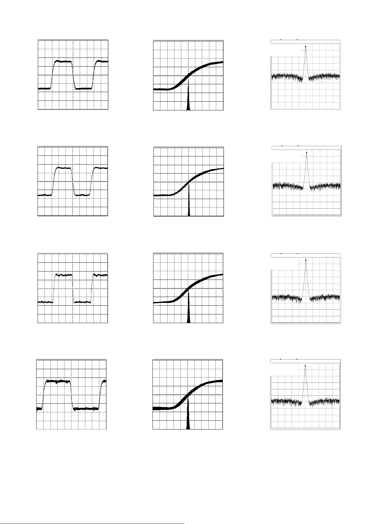
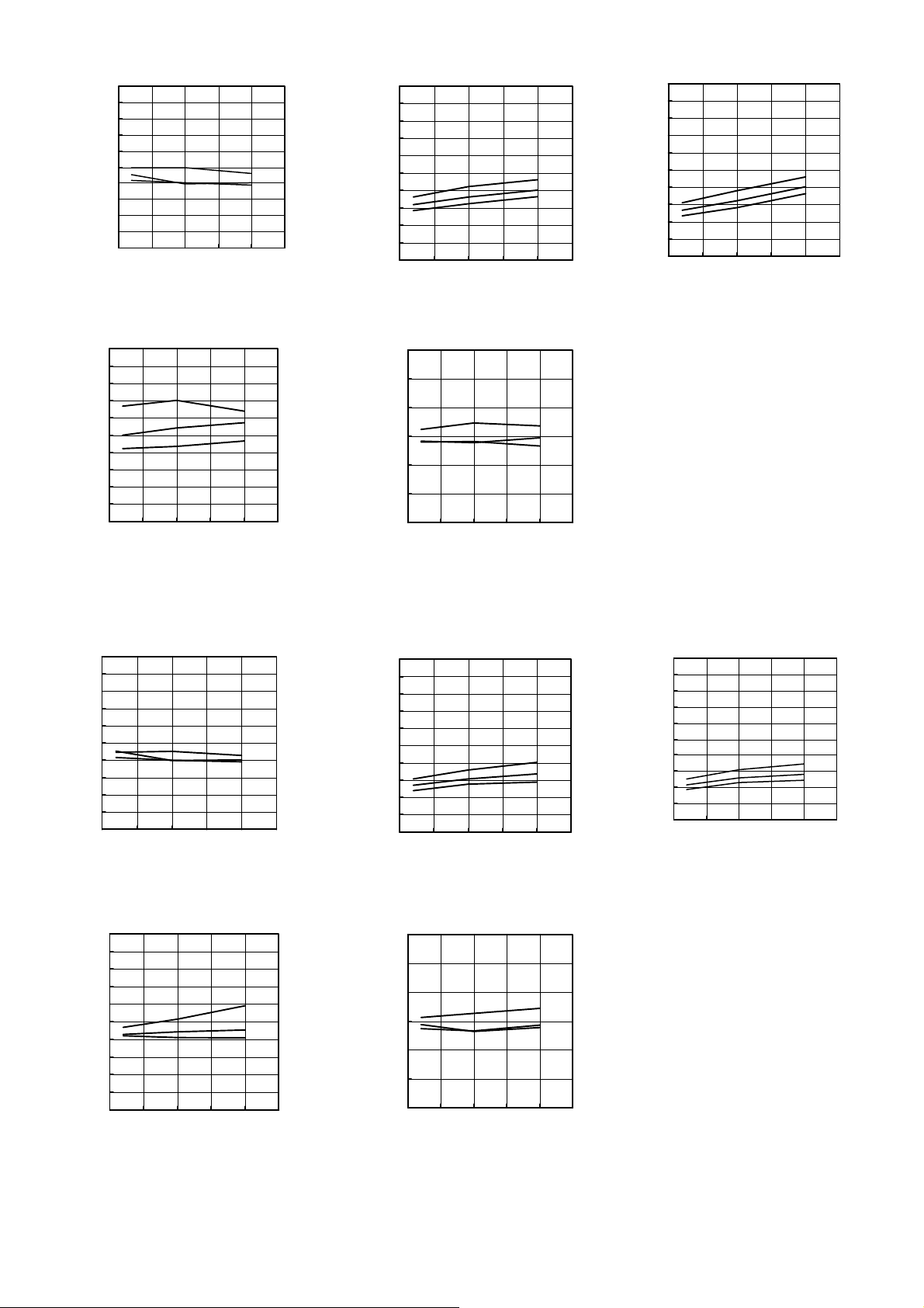
【Output waveform】
Duty Duty1 45 50 55 %Measured at a voltage of 1/2 of VDD
Rise time Tr -2.5 -nsec
Period of time required for the output
to reach 80% from 20% of VDD
Fall time Tf -2.5 -nsec
Period of time required for the output
to reach 20% from 80% of VDD
【Jitter】
Period-Jitter 1σP-J1σ-50 -psec
※1
Period-Jitter MIN-MAX P-J
MIN-MAX -300 -psec
※2
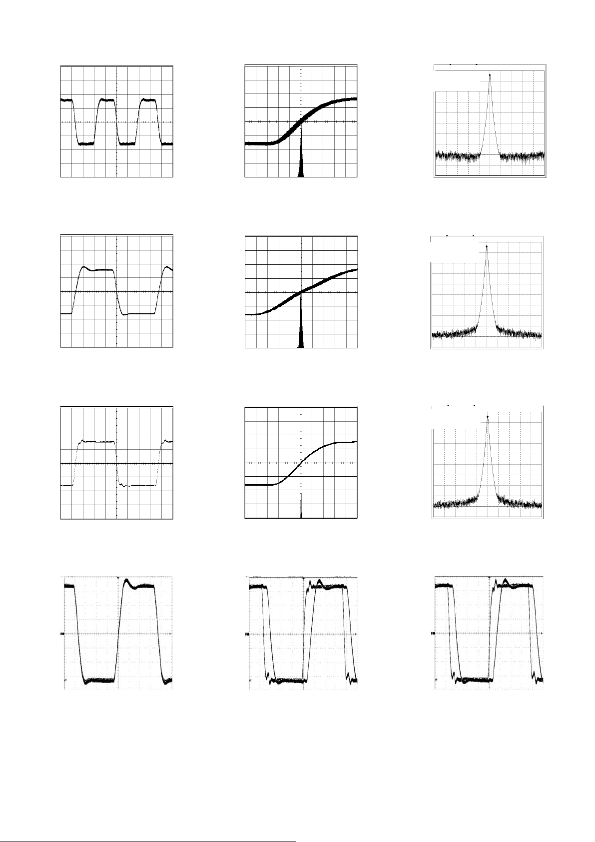
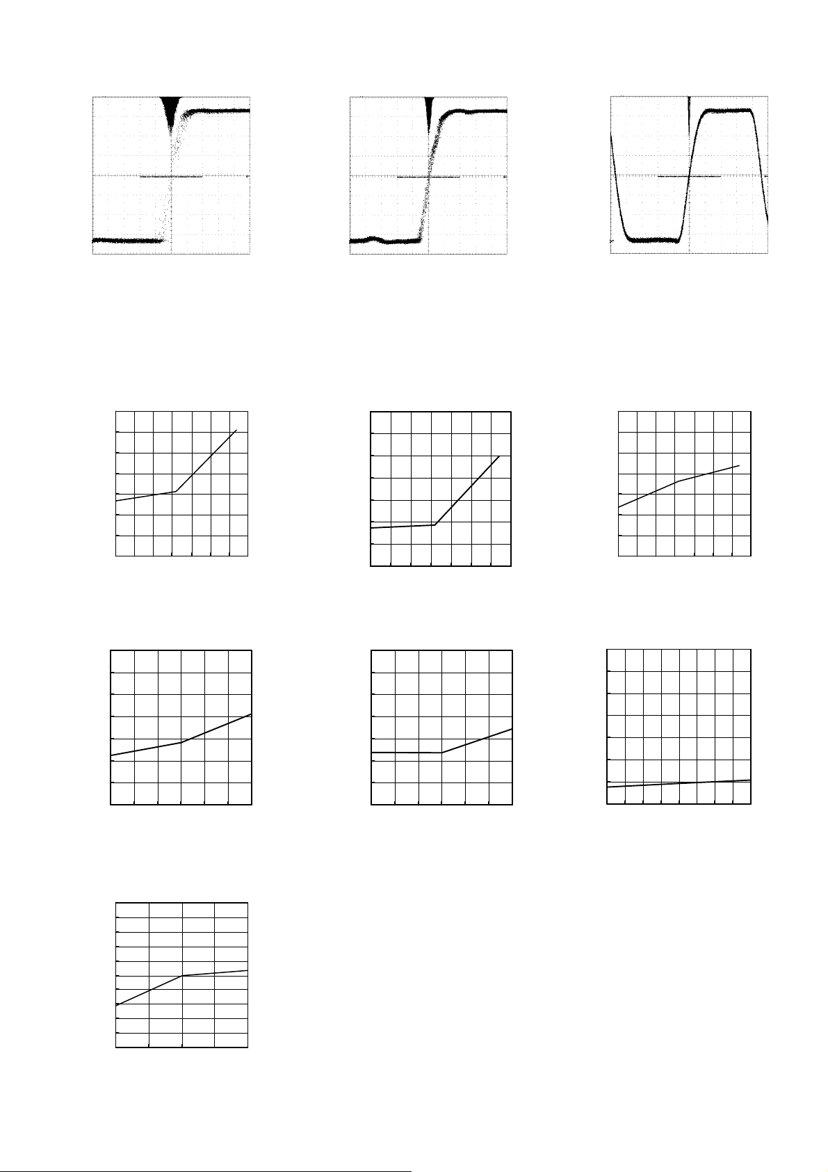
【Output Lock-Time】Tlock --1 msec
※3
【Frequency stability】ΔF/F0 -15 -15 ppm
T=-10~70 ℃、VDD=3.3V ±
0.15V ※4
【Frequency sensitivity】ΔF/Fc ±30 ±45 ±60 ppm
※5
【Frequency sensitivity linearity】Linearity -10 10 ppm
※5
【Buffer skew】Tskew
_BUF -500 -500 psec
Phase difference between
BUF_OUT1 and BUF_OUT26
【Buffer delay】Td_BUF -4 8 nsec
Phase difference between
BUF_IN and BUF_OUT
Note) The output frequency is determined by the arithmetic (frequency division) expression of a frequency input to XTAL_IN.