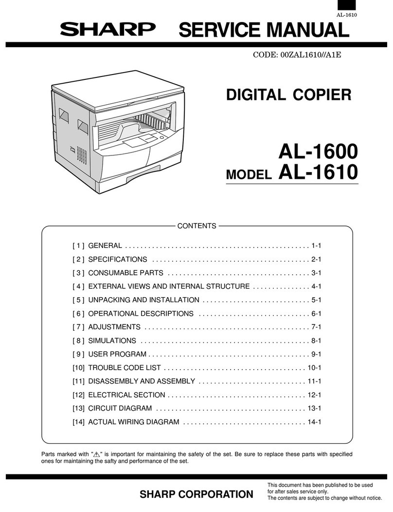
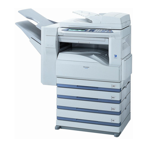
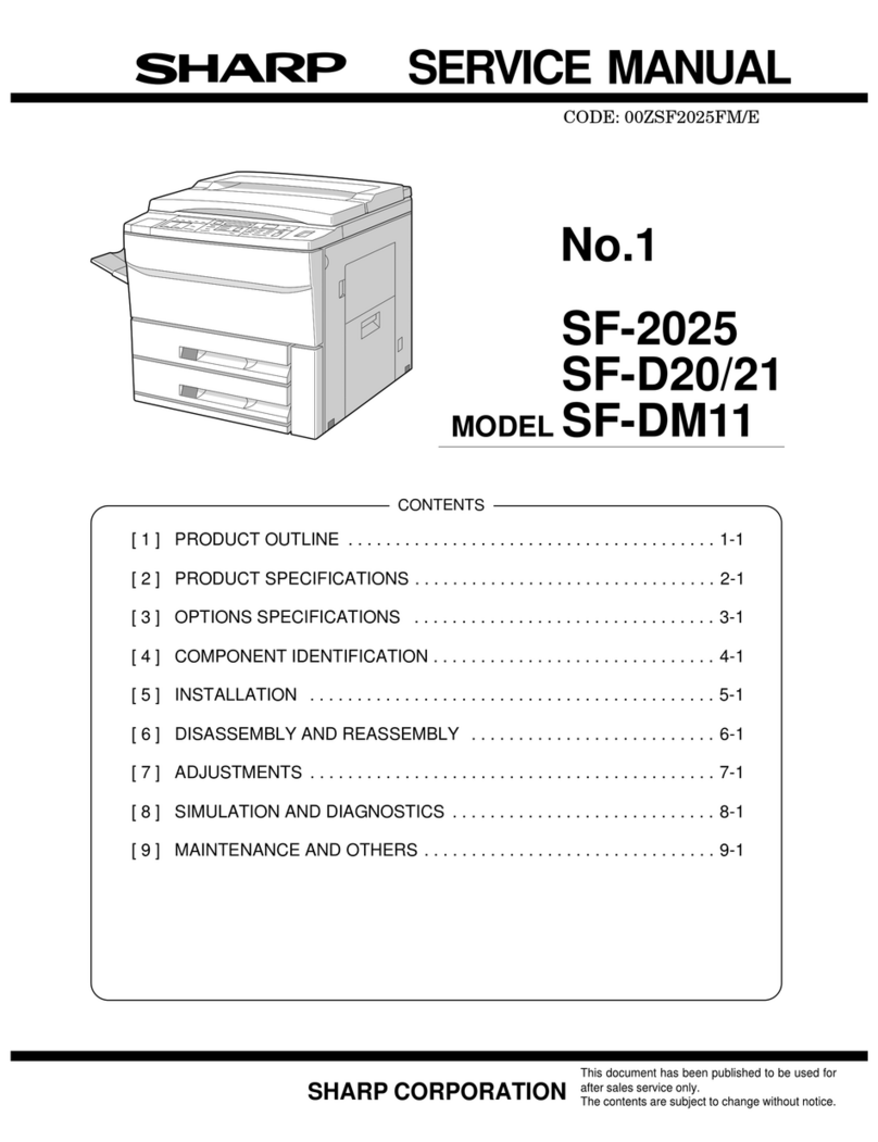
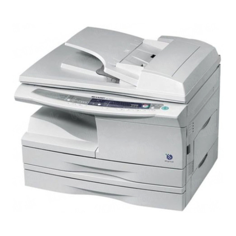
Sharp AR-5132 User manual

SERVICE MANUAL
CODE: 00ZAR5132TM1E
DIGITAL COPIER NO.2
MODEL AR-5132
[ 1 ] PRINCIPLES OF THE DIGITAL COPIER . . . . . . . . . . . . . . . . . . . 1-1
[ 2 ] PROCESS SECTION . . . . . . . . . . . . . . . . . . . . . . . . . . . . . . . . . . 2-1
[ 3 ] DEVELOPING SECTION . . . . . . . . . . . . . . . . . . . . . . . . . . . . . . . 3-1
[ 4 ] PAPER FEED SECTION . . . . . . . . . . . . . . . . . . . . . . . . . . . . . . . . 4-1
[ 5 ] TRANSPORT AND FUSING SECTION . . . . . . . . . . . . . . . . . . . . 5-1
[ 6 ] HIGH VOLTAGE SECTION . . . . . . . . . . . . . . . . . . . . . . . . . . . . . 6-1
[ 7 ] RADF MECHANISM SECTION . . . . . . . . . . . . . . . . . . . . . . . . . . 7-1
[ 8 ] DESK UNIT MECHANISM SECTION . . . . . . . . . . . . . . . . . . . . . . 8-1
[ 9 ] ELECTRICAL SECTION . . . . . . . . . . . . . . . . . . . . . . . . . . . . . . . . 9-1
[10] RADF ELECTRICAL SECTION . . . . . . . . . . . . . . . . . . . . . . . . . 10-1
[11] DESK UNIT ELECTRICAL SECTION . . . . . . . . . . . . . . . . . . . . . 11-1
SHARP CORPORATION
CONTENTS
This document has been published to be used
for after sales service only.
The contents are subject to change without notice.
Parts marked with "!" is important for maintaining the safety of the set. Be sure to replace these parts with specified
ones for maintaining the safety and performance of the set.

CAUTION
This copier machine is a class 1 laser product that complies with 21CFR 1040.10 and 1040.11 of the
CDRH standard and IEC825. This means that this machine does not produce hazardous laser
radiation. The use of controls, adjustments or performance of procedures other than those specified
herein may result in hazardous radiation exposure.
This laser radiation is not a danger to the skin, but when an exact focusing of the laser beam is
achieved on the eye’s retina, there is the danger of spot damage to the retina.
The following cautions must be observed to avoid exposure of the laser beam to your eyes at the time
of servicing.
1) When a problem in the laser optical unit has occurred, the whole optical unit must be exchanged
as a unit, not as individual parts.
2) Do not look into the machine with the main switch turned on after removing the developer unit,
toner cartridge, and drum cartridge.
3) Do not look into the laser beam exposure slit of the laser optical unit with the connector connected
when removing and installing the optical system.
4) The safety interlock switch is equipped.
Do not defeat the safety interlock by inserting wedges or other items into the switch slot.
CLASS 1
LASER PRODUCT
LASER KLASSE 1
LASER WAVE –LENGTH : 785 ±15nm
Pulse times :
Out put power : 0.3mW ∼0.6mW
CAUTION
INVISIBLELASER RADIATION,
WHEN OPEN AND INTERLOCKS DEFEATED.
AVOID EXPOSURE TO BEAM.
VORSICHT
UNSICHTBARELASERSTRAHLUNG,
WENN ABDECKUNG GEÖFFNET UND
SICHERHEITSVERRIEGELUNGÜBERBRÜCKT.
NICHT DEM STRAHL AUSSETZEN.
VARO !
AVATTAESSA JA SUOJALUKITUS
OHITETTAESSA OLET ALTTIINA
NÄKYMÄTTÖMÄLLELASERSÄTEILYLLEÄLÄ
KATSOSÄTEESEEN.
ADVARSEL
USYNLIG LASERSTRÅLNING VED ÅBNING, NÅR
SIKKERHEDSBRYDERE ER UDE AF
FUNKTION. UNDGÅ UDSAETTELSE FOR
STRÅLNING.
VARNING !
OSYNLIG LASERSTRÅLNING NÄR DENNA DEL
ÄR ÖPPNAD OCH SPÄRREN ÄR URKOPPLAD.
BETRAKTA EJ STRÅLEN. – STRÅLEN ÄR
FARLIG.

CONTENTS
[ 1 ] PRINCIPLES OF THE DIGITAL
COPIER . . . . . . . . . . . . . . . . . . . . . . . . . . . . 1-1
1. Difference in structure from analog copiers 1-1
2. Basic composition of the digital copier . . . . 1-1
3. Scanner section . . . . . . . . . . . . . . . . . . . . 1-2
4. Laser unit . . . . . . . . . . . . . . . . . . . . . . . . . . 1-2
5. Image process section . . . . . . . . . . . . . . . 1-4
[ 2 ] PROCESS SECTION . . . . . . . . . . . . . . . 2-1
1. Outline . . . . . . . . . . . . . . . . . . . . . . . . . . . . 2-1
2. Basic process and composition . . . . . . . . . 2-3
[ 3 ] DEVELOPING SECTION . . . . . . . . . . . . 3-1
1. Basic outline . . . . . . . . . . . . . . . . . . . . . . . . 3-1
2. Basic composition . . . . . . . . . . . . . . . . . . . 3-1
3. Basic operation . . . . . . . . . . . . . . . . . . . . . 3-1
[ 4 ] PAPER FEED SECTION . . . . . . . . . . . . 4-1
1. Basic outline . . . . . . . . . . . . . . . . . . . . . . . . 4-1
2. Basic composition . . . . . . . . . . . . . . . . . . . 4-1
3. Basic operation . . . . . . . . . . . . . . . . . . . . . 4-2
[ 5 ] TRANSPORT AND FUSING
SECTIONS . . . . . . . . . . . . . . . . . . . . . . . . . 5-1
1. Outline . . . . . . . . . . . . . . . . . . . . . . . . . . . . 5-1
2. Basic composition and functions . . . . . . . . 5-1
[ 6 ] HIGH VOLTAGE SECTION . . . . . . . . . 5-1
1. Outline . . . . . . . . . . . . . . . . . . . . . . . . . . . . 5-1
2. Basic composition . . . . . . . . . . . . . . . . . . . 5-1
[ 7 ] RADF MECHANISM SECTIONS . . . . 7-1
1. Operation flowchart . . . . . . . . . . . . . . . . . . 7-1
2. Document size detection . . . . . . . . . . . . . . 7-4
[ 8 ] DESK UNIT MECHANISM
SECTION . . . . . . . . . . . . . . . . . . . . . . . . . . 8-1
1. Operation flow chart . . . . . . . . . . . . . . . . . . 8-1
[ 9 ] ELECTRICAL SECTION . . . . . . . . . . . . 9-1
1. Block diagram . . . . . . . . . . . . . . . . . . . . . . 9-1
2. ICU PWB . . . . . . . . . . . . . . . . . . . . . . . . . . 9-2
3. PCU PWB . . . . . . . . . . . . . . . . . . . . . . . . . 9-6
4. Operation section . . . . . . . . . . . . . . . . . . . 9-16
5. LCD display section . . . . . . . . . . . . . . . . 9-17
6. DC power circuit . . . . . . . . . . . . . . . . . . . . 9-22
[10] RADF ELECTRICAL SECTION . . . . 10-1
1. General . . . . . . . . . . . . . . . . . . . . . . . . . . 10-1
2. Block diagram . . . . . . . . . . . . . . . . . . . . . 10-1
3. Operations . . . . . . . . . . . . . . . . . . . . . . . . 10-2
[11] DESK UNIT ELECTRICAL
SECTION . . . . . . . . . . . . . . . . . . . . . . . . . 11-1
1. Outline . . . . . . . . . . . . . . . . . . . . . . . . . . . 11-1
2. Block diagram . . . . . . . . . . . . . . . . . . . . . 11-1
3. Operational descriptions . . . . . . . . . . . . . 11-2

[1] PRINCIPLES OF THE DIGITAL
COPIER
1. Difference in structure from analog
copiers
The digital copier is composed of the scanner section and the printer
section. (Refer to the figures.)
In the digital copier, the reflected light is not directly radiated onto the
OPC drum as in the analog copiers.
2. Basic composition of the digital copier
Analog machine
Copy lamp section
Drum
CCD
Digital machine
Copy lamp section
Scanner
section
Laser section
Drum Printer
section
CCD
OPU
(Operation
panel section)
Serial
communication
PCU
(Process
Control Unit)
Serial
communication
Sorter
(Option)
Serial communication
Serial
communication
Fusing section
ADU
RADF
Scanner section
ICU (Image process unit)
LSU (Laser unit)
Process section
Laser beam
Paper transport section
ADU
Paper tray 1 Paper
feed
section
Option
Printer PWB
Interface PWB
Personal
computer
Manual paper
feed section
Lens
Paper tray 2
Paper tray 3 (LCC type)
1 – 1

(1) Basic operations of copying
1Image data are scanned in the scanner section and sent to the
image process (ICU) PWB.
2The data are converted into printable data in the circuit of the
image process (ICU) PWB.
3The data are printed in the printer section.
3. Scanner section
(1) How to scan an document
The scanner is provided with sensors which are arranged on one line.
These sensors scan a horizontal line of an document at a time and
the data are outputted sequentially. After completion of the line, the
next line is scanned. The operation is repeated until one page is
completed. The figure below shows that the images scanned by the
sensors are sent to the ICU PWB sequentially.
The direction of the lines is called the "main scanning direction" and
the direction of scanning the "sub scanning direction."
The above figure shows four elements in one line. Actually, however,
there are thousands of elements in one line. The light receiving ele-
ments called CCD are used.
The resolution is an index value to express the capacity of scanners.
The resolution shows how many light receiving elements are used in
one inch (dpi, dot per inch).
While the sub scanning direction is used to control the motor which
drives the optical system and to adjust the resolution to take in the
images.
(2) Basic structure of the scanner section
The scanner unit is the scanning section of the digital optical system.
The light from the halogen lamp (which is driven by the DC power to
suppress ripples) is reflected by the document and passed through
three mirrors and the reduction lens to form images on the CCD
elements (image sensors). This system is called the reduction type
image sensor system. The light image (photo energy) formed on the
CCD elements are converted into electrical signals (analog signals)
by the CCD elements (Photo conversion).The output signals (analog
signals) are converted into digital signals (A/D conversion) to perform
various image processes. The resolution at that time is 400dpi.
4. Laser unit
The image data sent from the ICU (image process PWB) are passed
to the LSU (laser unit) and converted into laser beams.
(1) Basic structure
The LSU unit is the writing section of the digital optical system. The
semiconductor laser is used as the light source. Images are formed
by the polygon mirror and the fθlens on the OPC drum.
The internal structure is shown in the figure on the next page. The
image data from the ICU are converted into DUTY signals for every
gradations (256 steps), and the semiconductor laser on the laser
emitting PWB is turned on/off according to the DUTY. The laser
beams are passed through the collimator lens, the slit, the cylindrical
lens, the polygon mirror, the fθlens, and the mirror to form images in
the shaft direction (main scanning direction) of the OPC drum. The
laser emitting PWB is provided with the APC (Auto Power Control) to
eliminate fluctuations in the laser power. The BD PWB serves to
measure the writing point for the laser.
(2) Composition
Effective scanning width: 302 mm
Resolution: 400 dpi
Beam diameter: main scanning 75 µm, sub scanning 90 µm
Image surface power: 0.3mW ∼0.6mW
Polygon motor: Brushless DC motor
No. of mirrors →6
1
2
3
4
5
5432
1
Sub scanning direction
Sensor scanning area
Main
scanning
direction
Original
Image data sent to the ICU PWB
To ICU PWB
1 – 2
LSU internal structure
Functions of major parts
1Collimator lens
Converges laser beams into parallel beams.
2Cylindrical lens
Corrects laser beams in the sub scanning direction by shift of the
surface of the polygon mirror.
3BD (Mirror, lens, PWB)
Detects the start timing of the laser scanning.
4fθlens
•Converges laser beams on a spot on the OPC drum.
•Equalizes the scanning speeds of laser beams at both ends
and at the center.
5Polygon mirror, polygon motor
Reflects laser beams at constant rotation.
6Semiconductor laser
Generates laser beams.
L.D
Side view
Polygon motor Mirror
Cover glass
Sub scanning direction
Collimator
lens Cylindrical
lens Lens
Drum
f
Θ
lens 1
f
Θ
lens 3
Drum
Mirror
f
Θ
lens 3
f
Θ
lens 2
Mirror for BD
lens
(Cylindrical lens)
Polygon
motor fan
drive PWB
Polygon
motor
Convergence
lens for BD
BD PWB
f
Θ
lens 1
Leser drive PWB
f
Θ
lens 2
a
≠
b
≠
c
ab
c
d = e = f
de
f
f
Θ
LENS
1 – 3

5. Image process section
Data flow (flowchart) Content
<Lamp light quantity adjustment>
1. Halogen lamp (145W)
The lamp is lighted by the DC power under the reference white plate.
2. 400dpi reduction line sensor (CCD)
The sensor receives the reflected light as photo energy from the shading plate (refer-
ence white plate), and converts it into electrical energy (analog voltage).
⇓
3. A/D convertor
The analog voltage is divided into 256 to convert into digital data, that is, the voltage is
converted into binary 8-bit data.
⇓
Actually, the white data before A/D conversion is about 4.0V, and the black data is about
1.1V. Therefore, the difference between about 4.0V of white and about 1.1V of black is
divided into 256 divisions to convert into digital data.
(Example: 1.1V →0, 4.0V →256, 2.55V →128)
4. Gate array
The digital data sent from the A/D convertor are inputted to the gate array temporarily.
5. SRAM
Stores the data.
6. CPU
Judges with the value written into the SRAM whether the light is too bright or too dark. If
the light is too bright, it decreases the halogen lamp voltage. If the light is too dark, it
increases the halogen lamp voltage. Procedures 1 ∼6 are repeated to set the light
quantity at the optimum level.
<Black level correction>
7. Halogen lamp (Black level correction)
For black level correction, data obtained by SIM 63-2 are used. (The data are stored in
the SRAM.)
8. CCD
Though the halogen lamp is off, a constant voltage is outputted from the CCD.
9. A/D convertor
The output voltage (analog voltage) is converted into a digital value. (The digital value
may be ideally zero, however it will not become zero because of variations between
machines.)
10. Gate array 1
The digital data sent from the A/D convertor are temporarily stored in gate array 1.
11. SRAM
Stores data.
12. CPU
Obtains the optimum black reference value from the black image data written into the
SRAM. In the hardware, the odd number pixels and the even number pixels in the main
scanning direction are treated in two separate channels. Therefore, two reference
values for the odd numbers and the even numbers are required.
13. Latch
The reference values of the odd numbers and the even numbers are stored in the latch.
14. D/A convertor
The black reference values stored in the latch are converted into analog voltages by the
D/A convertor.
The analog voltages are used as the black reference values (- reference) of A/D conver-
sion.
Procedures 8 ∼14 are repeated to obtain the optimum black reference values.
2.
1.
3.
GA1
4.
SRAM
5.
CPU
6.
<Lamp light quantity adjustment>
Halogen lamp (ON)
CCD
CCD PWB
A/D convertor
ICU PWB
CCD
8.
7.
9.
GA110.
SRAM
11.
CPU
12.
13.
14.
<Black level correction>
Halogen lamp <OFF>
CCD PWB
A/D convertor
ICU PWB
Latch
D/A convertor
Photo energy
Photo
diode
Accumulation electrode
Shift electrode
1 – 4

Data flow (flowchart) Content
<White level correction>
15. Halogen lamp
For white level correction, the halogen lamp is lighted at the voltage obtained in the light
quantity adjustment under the shading plate and the shading plate is scanned.
16. CCD
The reflected light from the shading plate is received by the CCD as photo energy and
converted into electrical energy (analog voltage).
17. The analog voltage is divided into 256 sections (0 ∼255) to be digital data.
18. Gate array 1
The digital data are inputted to gate array 1 and thinned out every 16 lines.
19. SRAM
Stores data. Thinning out every 16 lines is performed in order to minimize the bad effect
by dirt on the shading plate.
20. CPU
The optimum white reference of 5048 pixels in the main scanning direction is obtained
from the SRAM data. At that time, the correction of variations between odd/even num-
bers is performed as well as the correction of the halogen lamp and the lens. These
corrections are made in order to prevent against darkness at both ends. In addition, the
correction for variations between the document surface and the shading plate previously
obtained by SIM 63-2 is performed.
21. FIFO
The correction data of one line are stored in the line memory (FIFO).
22. D/A convertor
The correction data of FIFO are converted into analog values to be the white reference
value (+ reference) in 17. The white reference value is switched for every pixel.
<Document scanning>
23. Halogen lamp
The halogen lamp is lighted at the voltage obtained by procedures 1 ∼6 to radiate the
document.
24. CCD
The scanned image data are sent to the ICU PWB with the analog signals.
25. A/D convertor, D/A convertor, latch, FIFO
Procedures 1 ∼22 are performed at the specified timings such as turning on the power.
The values obtained in 1 ∼22, however, the black reference values of odd/even num-
bers are stored in the latch, and the white reference value is stored in the FIFO.
Therefore, shading correction is performed in copying. The white/black reference values
of the A/D convertor are switched for every pixel to correct unevenness of the optical
system and converted into digital values.
26. Gate array 1
Takes data of the density level of the scanned document.
A judgment is made whether the document is of A type (an document of characters with
much white area) or of B type (a photo document with much half tone area) or of C type
(newspapers with much background area) to select the most suitable look-up table for
density conversion.
27. CPU/SRAM
Converts the density.
For an document of A type, an LUT (look-up table) which provides clear characters is
selected. For an document of B type, an LUT which provides clear half tone images is
selected. For an document of C type, an LUT which removes background. Since
process is performed for every several lines. the most suitable LUT may not be selected
for some documents. In that case, the manual exposure mode is selected.
CCD16.
15.
17.
GA118.
SRAM
19.
CPU
20.
21.
22.
FIFO
<White level correction>
Halogen lamp <ON>
CCD PWB
A/D convertor
ICU PWB
D/A convertor
CCD
24.
23.
25.
GA126.
CPU
FIFO
27.
<Document scanning>
Halogen lamp
CCD PWB
A/D convertor
D/A convertor
Latch
Histogram
ICU PWB
Density
conversion LUT
<ON>
Density value A Density value B Density value C
1 – 5

Data flow (flowchart) Content
28. FIFO
Image data of one line are stored in the line memory (FIFO). This FIFO is for zooming.
For reduction, the scanned image data are thinned out when they are written into the
FIFO. For enlargement, the scanned image values are used as the values of plural
pixels of the next one.
29. Gate array 2
Gate array 2 outputs the control signal to the FIFO to perform reduction and enlarge-
ment. Interpolation is also performed, which eliminates notches generated in enlarge-
ment. Two neighboring pixels before enlargement are interpolated primarily to eliminate
notches.
: Density of pixel in normal ratio ( 0 ∼255)
d1: Position if a pixel to be inserted.
C: Density of the pixel which was formed by interpolation. (0 ∼255)
⇓
C: (1 – d1) ×+ d1 ×
Example 1: Calculation of interpolation
Supposing that the density of at the normal ratio is 100 and that the density of is
200, and that the position of new pixel C after zooming is at 50% position, the density of
C is as shown below.
= (1 – 0.5) ×100 + 0.5 ×200
↓↓↓↓
d1 A d1 B
=150
↓
Density of new pixel C
Example 2: In the case of enlargement
In the case of enlargement of 200%, the image process is made so that the number of
pixels will be twice as greater as the number of the scanned pixels.
In short, the number of pixels scanned in the normal mode is duplicated to enlarge to
200%. One pixel in the normal mode is duplicated to two pixels in 200%. (Refer to the
description below.)
Then the density of pixels newly formed in the image process is determined. As shown
in example 1, the position of newly made pixel is at the center (50% position) of two
pixels scanned in the normal mode and the primary interpolation is performed as fol-
lows:
A= BC= A+ DE= DF= D+G
22
In the image process, enlargement is performed only in the main scanning direction. In
the sub scanning direction, the scanning sped of the optical system is changed to
perform enlargement. (For example in 200% enlargement, the scanning speed is
changed to 1/2, and 50% enlargement is performed by duplicating the scanning speed.)
The main scanning is performed by image process, and the sub scanning by varying the
speed of the optical system. Zooming in the main scanning direction is separately
performed from zooming in the sub scanning direction.
FIFO28.
29.
GA2
(Zooming)
ICU PWB
B
C
A
d1
D5
D6
D5 D6
D5
D6
B
C
A
d1
0
100 200
0.5
(50%)
D7
B
C
A
(200%)
D
E
F
G
H
I
(Normal)
1 – 6

Data flow (flowchart) Content
30. FIFO
This line memory (FIFO) is used for area separation and MTF correction.
31. Gate array 2
Performs area separation. In area separation, the characteristics of the target pixel and
the neighboring pixels are judged to perform the optimum process. For example, judge-
ment is made to identify that the area is a photo area or a hatched area such as
newspaper photos.
32. Gate array 2
Corrects blurs in images in the main scanning direction and the sub scanning direction.
Details are as follows.
MTF meas Modulation Transfer Function of the optical system.
a: Theoretical value
b: Value received by the CCD element (N)
The optical system provides out of focus even the focus adjustment is perfectly com-
pleted. When the CCD elements receive reflected light from the document, the light
leaks to the neighboring pixels by the optical system characteristics. On the contrary,
light come in from the neighboring pixels. Correction is made by adding the leaked lights
and subtracting the lights from the neighboring pixels. This correction is called the MTF
correction.
(In actual, this process includes calculation of the effect on the pixels by the preceding
and the following lines.
The MTF correction performs process to provide clear characters by edge emphasis if
the area separation result is a character area, and to provide less emphasis if the result
is a hatched area, and to provide smooth images if the result is a photo area.
When the soft photo mode is selected, the area separation and the MTF correction are
not performed, but the multi-value dithering is performed instead. The size of dither
matrix in multi-value dithering can be selected by simulation.
33. Gamma correction SRAM
Gamma correction is performed to make optimum copying of image data. In the photo
mode, gamma correction is made to reproduce clear half tone images. In the manual
mode, gamma correction is performed to provide clear copying of characters.
Image data before correction are of 8 bit as well as image data after correction. (0 ∼
255)
In the photo mode, line alignment is performed, where the gamma correction curve of
the odd number pixels and the even number pixels in the main scanning direction are
changed to reduce fluctuations in drive of the machine.
In combination with the above area separation, it reduces bad effects of line alignment
process for hatched documents.
The gamma correction SRAM performs the highlight process.
34. Laser pulse width modulation
The image data which are subjected to the gamma correction are converted into laser
pulse signals (which varies the laser radiating time for each pixel.)
Radiating time of laser can be changed in the unit of 1/256.
35. ECL circuit
The laser pulse width signal is sent to the LSU at ECL level.
36. LSU
The laser scan unit performs printing.
30.
31.
FIFO
32.
33.
35.
34.
36.
GA2
GA2
(Area
separation)
(MTF
correction)
ICU PWB
Gamma
correction SRAM
(Irregular drive
countermeasure)
Laser pulse
width modulation
ECL circuit
LSU
CCD
a
b
Original
1 pixel (N)
1 – 7

(2) Image process section
The image process section is composed of gate arrays A and B, the
CPU, and memories (SRAM, FIFO, EPROM). Gate array A forms
data for shading correction and calculates histogram data for auto-
matic exposure. Gate array B performs area separation, filter
process, address generation for self printing, multi-value dithering,
and electronic zooming of main scanning.
The CPU performs register setting and rewriting of LUT (look up
table) every time when the user changes the mode. It also calculates
the correction value of shading correction.
The figure below shows the flow of image signals.
ICU image process section block diagram
[Shading correction]
The analog image data from the CCD PWB are inputted to the CCD
control section in the ICU and converted into digital data, and passed
through gate array A in the ICU image process section, and written
into the multi-function LUT (Look Up Table). (Path shown with dotted
line in the above diagram.)
Gate array A performs thinning out of 16 lines at that time. Thinning
out of 16 lines is performed when there is dirt on the shading plate.
[Auto exposure]
The analog image data from the CCD PWB are inputted to the CCD
control section in the ICU and corrected by the shading data obtained
from the above method and converted into digital data and inputted to
gate array A. In gate array A, the total number data (simple his-
togram) of pixels in each density is calculated as shown in 1-5. The
calculated data are used to judge that the document is of background
type such as newspapers or of half tone type such as photos or of
white type with less black and without half tone such as character
documents. The data are calculated for each line. According to the
data, the CPU selects the most suitable density conversion look up
table from 32 kinds of density conversions look up tables in the
density conversion LUT.
[Electronic zooming]
The image data, after auto exposure and the visual sensitivity correc-
tion, are written into the FIFO for enlargement. Gate array B controls
the enable signal for reading the enlargement FIFO to thin out the
read data, enlarging images. For example, in enlargement of 200%,
the read enable signal is provided for every pixel to make enlarge-
ment. The image data thinned out for enlargement are inputted to
gate array B and the primary interpolation is performed as shown in
1-6. (For details, refer to 1-6.) The image data thinned out primarily
are written into the reduction FIFO. The enable signal for writing is
controlled to thin out for reduction.
[Area separation]
After electronic zooming, the image data are written into the FIFO for
area separation/filter/multi-value dithering. There are four FIFO’s and
each one sends data for one line. Therefore gate array B can input
image data of five lines. Gate array B calculates the characteristic
value of peripheral pixels according to the image data of five lines
and the result is outputted to the address of the multi-function LUT.
The multi-function LUT is the same one described in the shading
correction. When the are separation mode is selected, the CPU reads
the data for area separation from the EPROM (for data) and write into
the multi-function LUT.
FIFO FIFO
FIFO
FIFO
FIFO
FIFO
CPU
H8/3040
10MHz
EPROM
(program)
64K x 8
EPROM
(data)
256K x 8
SRAM
(work)
32K x 8
Shading
correction data
ICU
CCD
control
section
Image
data
Density
conversion
LUT
SRAM
8K x 8
Visible sensitivity correction
Automatic exposure
Gate array A
Shading correction data
forming
Histogram data calculation
for automatic exposure
5K x 8bit
FIFO for
enlargement
Electronic
zoom
5K x 8bit
FIFO for
reduction
Image data
Gate array B
5K x 8bit
FIFO for area separation
multi value dither
Image data for calculation of shading correction data
Multi function
LUT
Filter
process
(MTF
correction)
ICU
laser control
section
Gamma correction
LUT
Area
separation
Multi value
Dither
Self print
SRAM
32K x 8
Area separation data,
self print data, multi
value dither data,
shading correction
data by the neural
net
Gamma
correction
Black/white
reverse
Line
alignment
SRAM
8K x 8
1 – 8

[MTF correction]
When the characteristic value outputted from gate array B is inputted
to the address of multi-function LUT, data which show the charac-
teristics of the peripheral pixels are outputted from the multi-function
LUT. For example, the data show that the pixel and the peripherals
are characters and edged of line drawing or that they are part of a
hatched image of photo in a newspaper or that they are part of a
photo of continuous gradation (that is not a hatched photo). Filter
process is performed according to each pixel’s characteristics.
[Gamma correction/line alignment/black-white highlight]
After the MTF correction, the image is subject to the gamma correc-
tion in order to cope with the OPC drum characteristics, the develop-
ing characteristics, and the actual copy density. Before copying, the
CPU reads the density conversion look up table value corresponding
to the value which was set by the user with the density adjustment
key from the EPROM (data), and writes the data into the gamma
correction LUT (SRAM). The image data are connected to the lower 8
bits of the gamma correction LUT address and converted by the look
up table. Black-white highlight is performed at the same time.
[Soft photo mode]
This is the multi-value dithering mode which has been newly added
from this mode. The area gradation is combined with the pulse width
modulation to improve the gradation of photo. The size of area grada-
tion (dither matrix) can be selected with simulation.
[Self printing mode]
Gate array B prints out the test pattern by outputting the address
count values of main scanning and sub scanning.
Gate array A
Pin arrangement table
No. Pin name I/O Function
1 GND
2
*
7
RAMADR0
*
RAMADR5
O
*
O
Data bus to the peripheral memory
connected to this LSI.
8 VDD
9 RAMADR6 O Data bus to the peripheral memory
connected to this LSI.
10 RAMADR7 O
11 GND
12 RAMADR8 O Data bus to the peripheral memory
connected to this LSI.
13 GND
14 VDD
15
*
20
RAMADR9
*
RAMADR14
O
*
O
Data bus to the peripheral memory
connected to this LSI.
21 FINAL O Signal which shows the end of shading
correction.
22 GND
23
*
30
RAMADR0
*
RAMADR7
I/O
*
I/O
Address bus to the peripheral memory
connected to this LSI.
31 GND
32
*
42
XIFDAT0
*
XIFDAT7
I/O
*
I/O Data bus to set the built-in register.
43 GND
44
*
53
SHADOUT0
*
SHADOUT7
I/O
*
I/O
Signal to output the data after shading
correction.
54 GND
No. Pin name I/O Function
55
*
60
XIFADR0
*
XIFADR5
IN
*
IN Data bus to set the built-in register.
61 RAMRD OUT Read signal to the peripheral memory.
62 VDD
63 GND
64 WCLK OUT Not used.
65 CLK1 IN System clock of this LSI. Clock of
16MHz is inputted.
66 XIFEN IN Data enable signal to the built-in
register.
67 XIFRD IN Data read signal to the built-in register.
68 XIFWR IN Data write signal to the built-in register.
69 RESET IN Initializes the LSI.
70 VDD
71 CLK2 IN System clock of this LSI. Clock of
16MHz is inputted.
72 RAMWR OUT Write signal to the peripheral memory
73 HSYNC IN Image data 1 line read start signal.
74 PAGE IN Signal which shows the effective area
of one page of image data.
75 RESERVE
Not used.
76 RESERVE
77 RESERVE
78 RESERVE
79 GND
80 RESERVE
Not used.
81 RESERVE
82 RESERVE
83 RESERVE
84 GND
85
*
87
H0
*
H2
OUT
*
OUT Not used.
88 VDD
89 GND
90
*
92
V0
*
V2
OUT
*
OUT Not used.
93
*
100
ADIN0
*
ADIN7
IN
*
IN Image data bus
1 – 9

Gate array B
Pin arrangement table
No. Pin name I/O Function
1 GND
2 VCC
3
*
10
AIN0
*
AIN7
IN
*
IN (n) Line image data input pin.
11
*
14
RAMADR0
*
RAMADR3
OUT
*
OUT
Signals according to each mode
such as the result of area separation
are outputted to the external LUT
from this pin.
15 GND
16
*
19
RAMADR4
*
RAMADR7
OUT
*
OUT
Signals according to each mode
such as the result of area separation
are outputted to the external LUT
from this pin.
20 VCC (fixed)
211 GND (fixed)
22 GND
23
*
30
BIN0
*
BIN7
IN
*
IN (n+1)the line image data input pin
31 RESERVED Not used.
32
*
34
RAMADR8
*
RAMADR10
OUT
*
OUT
Signals according to each mode
such as the result of area separation
are outputted to the external LUT
from this pin.
35 GND
36
*
39
RAMADR11
*
RAMADR14
OUT
*
OUT
Signals according to each mode
such as the result of area separation
are outputted to the external LUT
from this pin.
40 GND
41
*
48
RAMDATA0
*
RAMDATA7
IN
*
IN
Pin for data input from the external
LUT.
49
*
52
FILOUT0
*
FILOUT7
OUT
*
OUT
Pin for output of the result of filter
process.
53 GND
54
*
57
FILOUT4
*
FILOUT7
OUT
*
OUT
Pin for output of the result of filter
process.
58 CLK1 IN Clock signal input pin. Clock of
16MHz is inputted.
59 GND
60 VCC
61 GND (fixed)
62 VCC (fixed)
63
*
70
CIN0
*
CIN7
IN
*
IN (n+2)the line image data input pin
71
*
78
XIFDAT0
*
XIFDAT7
I/O
*
I/O Data bus to set the built-in register.
79 GND
80
*
87
DIN0
*
DIN7
IN
*
IN (n+3)the line image data input pin
88 RESET IN Reset signal of the LSI
89
*
94
XIFADR0
*
XIFADR5
IN
*
IN
Address bus to select the built-in
register.
No. Pin name I/O Function
95 AREALDLY OUT Signal showing the effective image
area which is behind from AREA
signal by 4 clocks. LOW active.
96 CLK2 IN Clock signal input pin. Clock of
16MHz is inputted.
97 XIFRD IN Data read signal to the built-in
register.
LOW active.
98 XIFWR IN Data write signal to the built-in
register. LOW active.
99 XIFEN IN Data enable signal to the built-in
register. LOW active.
100 VCC (fixed)
101 GND (fixed)
102
*
105
BUNRIOUT0
*
BUNRIOUT3
OUT
*
OUT Area separation test pin.
106 GND
107
*
112
BUNRIOUT4
*
BUNRIOUT9
OUT
*
OUT Area separation test pin.
113 GND
114 CLK3 IN Clock signal input pin. Clock of
16MHz is inputted.
115
*
125
ZOOMIN0
*
ZOOMIN10
IN
*
IN Zooming process data input pin.
126 GND
127
*
130
ZOOMOUT0
*
ZOOMOUT3
IN
*
IN Zooming process data input pin.
131 GND
132
*
135
ZOOMOUT4
*
ZOOMOUT7
IN
*
IN Zooming process data input pin.
136 GND
137 VCC
138
*
140
ZOOMOUT8
*
ZOOMOUT10
IN
*
IN Zooming process data input pin.
141 FIFOWEN OUT Write enable signal to the line
memory. LOW active.
142 VCC (fixed)
143 GND (fixed)
144 GND
145 FIFOREN OUT Read enable signal to the line
memory. LOW active.
146
*
148
RAMDLY0
*
RAMDLY2
OUT
*
OUT
10-clock behind signal of
RAMDATA0 ∼2.
149 AREAHDLY OUT Signal showing the effective image
area which is behind from AREA
signal by 5 clocks. LOW active.
150 HSYNC IN Image data 1 line scanning start
signal
151 AREA OUT Signal which shows the effective
image area. LOW active.
152
*
159
EIN0
*
EIN7
IN
*
IN (n+4)the line image data input pin.
160 PAGE IN Signal which shows one page of
image data. LOW active.
1 – 10

[2] PROCESS SECTION
(OPC drum, cleaning unit)
1. Outline
The indirect electrostatic copiers use normal paper for copying, and
form electrostatic latent images on the OPC drum surface which can
be used repeatedly, develop them into visible images (toner images),
and transfer them on copy paper. Copies are made indirectly in the
copier of this type.
The PPC (Plain Paper Copier) makes copies in six processes: charg-
ing, exposure, developing, transfer, discharging, and cleaning which
cleans the OPC drum surface to use is repeatedly after transfer.
(1) Image forming process
1The OPC drum is charged.
2The OPC drum is exposed to form electrostatic latent images.
3Toner is attracted to the electrostatic latent images.
4The developed toner images are transferred on recording media
such as paper.
5Residual toner remaining on the OPC drum surface is cleaned.
6Residual charges on the OPC drum are removed.
(2) OPC drum
Some materials conduct electricity, and some others do not. The
materials are divided into three groups according to their conductivity:
conductors, semiconductors, and insulators.
This classification is not strict, and it is difficult to classify the
materials strictly.
Generally speaking, the materials with resistivity of 108Ωcm or
above are called insulators. Those with resistivity of 10–3 Ωcm or
below are called conductors.
The materials between the two are generically called semiconductors.
The conductors are always conductive. The semiconductors are nor-
mally not conductive, but under a certain condition become conduc-
tive.
The photoconductor used in the copiers are insulators when they are
not exposed with light, and reduce the resistivity when they are ex-
posed with light, that is, they become conductive (by the photo con-
ductivity phenomenon) when exposed with light. They are also called
as photo semiconductors and used in the copiers.
(3) Kinds of photoconductors
Major photo conductive materials used in the copiers are zinc oxide
(ZnO), amorphous selenium (amorphous Se) alloy, cadmium sulfide
(CdS), amorphous silicon (amorphous Si), and organic photoconduc-
tor (OPC).
The compositions of photoconductors used in the copiers are shown
below.
Zinc oxide (ZnO) master
Cadmium sulfide (CdS) drum
Organic photoconductor (OPC) master or drum
Selenium (Se) drum)
1
2
3
4
5
6
Charging
Exposure
Developing
Transfer
Cleaning
Discharging
OPC drum
CTL
CGL
Base
Dark area Dark area Light (Laser)
Principle of photoconductor (conductivity)
Non0organic
photoconductor
Organic
photoconductor
Amorphous selenium (non crystal Se)
Selenium alloy
Zinc oxide (ZnO)
Cadmium sulfide (CdS)
Amorphous silicon (Non crystal Si)
Organic photoconductor (OPC)
Photoconductive layer (zinc oxide layer)
Intermediate layer
Paper
Back coating paper Base paper
PET layer
Micro space layer
Photoconductive layer (CdS layer)
Aluminum layer
Carrier transfer layer
Carrier generation layer
Organic photo
conductive
layer
(OPC layer)
Aluminum layer
(selenium layer)
Photoconductive layer
Aluminum layer
2 – 1

Characteristics of organic photoconductors (OPC)
•Can be formed into various shapes (drum, sheet, belt)
•High insulation in a dark place. (Acceptability and retainability of
charges)
•Light weight
•Stable against humidity and temperature
•Safe and clean to the environment (harmless)
•Weak in wear by friction
•Weak in durability against light and ozone
(4) Characteristics of photoconductors
The important characteristics of photoconductors are as follows:
1. Photo sensitivity 2. Spectrum characteristics
3. Acceptance potential 4. Charge retainability
5. Residual potential 6. Fatigue
[Photosensitivity]
It is determined by the attenuation speed of the potential when ex-
posed with light.
[Spectrumcharacteristics]
The sensitivity of photoconductors differs depending on the kind and
the waveform of light.
Relationship between color and waveform
Human eyes can feel the lights with waveform of 380nm to 780nm.
These are called "Visible lights." The light whose waveform is shorter
than that is called "Ultraviolet light." The light whose waveform is
longer than that is called "Infrared light."
The figure below shows the relationship between lights and
waveforms.
[Acceptancepotential]
The dark resistance of the photoconductor layer decreases as the
electric field applied between layers increases.
When the photoconductor is charged, the electric field is formed to a
high level and the resistance of the layer decreases to restrict the
charging amount of the photoconductor. The potential of the
photoconductor at that time is called the acceptance potential, which
serves as an important factor to determine the potential contrast. The
photoconductor is generally charged to a potential slightly lower than
the acceptance potential in order to avoid applying an electrical strain
to the photoconductor.
[Chargeretainability]
The retaining time of electrostatic latent images on the photoconduc-
tor is determined by the speed of decrease in the potential in a dark
place. That is, it is measured with the time for the photoconductor
potential to decrease to the half of the initial level. This retainability of
electrical charge makes a problem when the interval time between
exposure and developing is longer. In the machines where a series of
operations of charging, exposure, and developing are automated, the
interval between the processes is short enough and there is no
problem.
[Residual potential]
When the charged photoconductor is exposed, the potential is rapidly
attenuated at first then slowly. The potential where this slow attenua-
tion starts is called the residual potential. The lower the residual
potential is, the greater the voltage contrast is. Therefore, the lower
residual potential is desirable.
[Fatigue]
When the photoconductor is charged and exposed repeatedly, it is
fatigued. Fatigue of the photoconductor results in increase in attenua-
tion speed of the photoconductor potential and decrease in the
retainability of charges.
In the above, the necessary characteristics for the photoconductors
are described. In an actual machine, when charging is repeated by
the charger, dust and dirt or splashed toner may be attached to the
saw tooth. These are not resulted from uneven charging, and they
should be removed by cleaning.
1.0
400
0.8
0.6
0.4
0.2
500 600 700 800
Se:Te
900
Sensitivity
Amorphous silicon OPC for digital
OPC for
analog
Wavelength (nm)
Spectrum sensitivity
350 400 450 500 550 600 650 700 750 800
Blue green
Violet
Blue
Green
Yellow
Orange
Red Infrared
Ultraviolet
2 – 2

2. Basic process and composition
•This machine employs the scorotron system to charge the
photoconductor surface uniformly to a certain level. The conven-
tional corona charger mechanism is employed which is composed
of the corona wire and the saw tooth plate (stainless plate of
0.1mm thick).
In corona charging, oxygen molecules in the air are ionized to form
ozone. This mechanism suppresses the generation of ozone.
•The process separation mechanism is employed for serviceability.
•The one-touch stopper mechanism prevents against high voltage
leakage caused by drop of the corona charger unit.
(1) Details of image forming process
Step 1: Charging
Main charger high voltage transformer (MHVG)
Grid voltage Developing bias
voltage
Standard mode –490V –400V
Photo mode –490V –400V
TSM mode –440V –350V
Printer mode –460V –400V
A uniform negative charge is applied to the OPC drum surface by
negative corona discharge of the main charger.
The OPC drum surface potential is controlled by the screen grid
voltage to be virtually the same level as the grid voltage.
•When the drum surface potential is lower than the grid voltage,
electric charges generated by discharging of the main charger are
passed through the screen grid to keep charging until the drum
surface potential reaches the same level as the grid voltage.
•When the drum surface potential reaches about the same level as
the grid voltage, electric charges generated by discharging of the
main charger flow through the electrode of the screen grid to the
high voltage unit grid voltage output circuit. Therefore the drum
surface potential is kept at the same level as the grid voltage.
Step 2: Exposure (laser beams)
Laser beams are generated in the LSU according to the print signal
from the ICU and radiated to the drum surface. The resistance of the
are of OPC layer where laser beams are radiated reduces to dis-
charge negative charges, forming electrostatic latent images on the
drum surface.
Step 3: Developing (Bias –400V)
The electrostatic latent images on the drum surface are made visible
images. This model uses the two-component magnetic brush
developing system to supply the bias voltage of –400V to carriers
(MG roller), and toner is negatively charged by friction with carriers.
Since the non-image area on the drum is negatively charged greater
than the developing bias, the negatively charged toner is repulsed
from the drum. The image area on the drum is exposed by laser
beams and its potential is decreased. Then negative toner is attached
to it by the DV bias.
( 5.25KV)
LD
785nm
400V
EXP
MC
DV
unit
( 5.3KV)
TC
I t 180µA
SC
AC 5.2KV
(DC 400V)
DL
Fuse bulb
Drum mark
sensor
Toner
Carrier
Developing bias
Process
control
sensor
Drive system view
Screen grid
Main charger output
section
Grid voltage output section High voltage
unit
Exposure
Exposure (laser beam)
OPC
layer
Pigment
layer
Aluminum
layer
(drum) Non image
area Image
area
Non image
area Image
area
N
S
S
N
N
-400V
Carrier
Toner
2 – 3

Step 4: Transfer
The visible images on the drum surface are transferred to copy
paper. Positive corona of the transfer charger is applied to the back of
the copy paper to transfer toner on the drum to the copy paper.
Step 5: Separation
Since the copy paper is positively charged and the drum is negatively
charged after transfer, an attraction force is generated between the
drum and the copy paper. Then an AC corona overlapped with nega-
tive DC is applied to the copy paper to decrease the copy paper
potential to the same level as the drum surface potential. Therefore
an attraction force between the drum and the copy paper disappears,
and the copy paper is separated by its own flexibility. If the paper is
not separated by the separation charger, it is forcibly separated by
the separation pawl.
Step 6: Cleaning
Residual toner on the drum is removed by the cleaning blade.
Step 7: Discharge
The discharge lamp light is radiated to the drum to reduce the electric
resistance of the OPC layer, eliminating the residual charges.
(3) Potential transition of the DV unit section
Toner
Paper guide
Copy paper
Transfer charger
output section
High voltage unit
Separation
pawl
Copy paper
Separation charger
output section
High voltage unit
Cleaner blade
Residual toner
Discharge lamp
0Start
D.S.P.
DV.Bias 0V
ON
0V -400V
D.S.P.
DV.Bias -550V
OFF -550V
D.S.P.
DV.Bias -70V
ON -70V -400V
D.S.P.
DV.Bias -550V
ON -550V -400V
0V
(-V)
Toner
attachment
potential
Print potential
Developing bias
Drum surface potential
Toner attachment
Carrier attachment
Image area
Non image area
Drum
Time
MG roller
Toner
Carrier
DSP: Drum surface potential
2 – 4
(4) OPC drum sensitivity reduction correction
In the AR-5132, deterioration of copy quality is prevented by correc-
tion with the charging grid voltage against the potential reduction of
the OPC drum due to repeated use.
The drum wear increases the grid voltage to maintain the drum sur-
face potential at a constant level, and the apparent sensitivity of the
OPC drum is decreased. To correct this, the laser beam strength is
increased when the coefficient of the drum rotating time for correction
of the charging grid voltage reaches a certain level.
(5) Process control function
[Outline]
The density of the reference toner image formed on the OPC drum
surface is used as the standard patch density, and the developing
bias and the charging grid voltage are controlled to provide the same
density as the standard patch density for stabilizing the copy images.
That is, the process conditions are set, and the high voltage output is
changed and corrected so that the toner density is stabilized under
the conditions.
Process control
1Toner patch images are formed on the OPC drum surface under
the three kinds of conditions (MC grid bias voltage) and the
developing bias. (The voltage is an actually measured value.)
In the process control, toner patch images are formed at the laser
output of the reference grid voltage (–410V) and the developing
bias (–240V) ±50V and duty of 100%.
2The three kinds of toner patch images and the drum surface are
measured with the process density sensor to obtain the relation-
ship between them.
OPC drum
Cleaner
section Developing
section
R
F
Main control PWB
CPU density
judgement
I/O MC grid
developing bias
output selection
Process density
sensor PWB
Density detection
level setting (VR2)
High voltage PWB
Each mode MC
grid developing
bias output
(density correction)
(Light quantity
correction)
CTL
CGL
CTL
CGL
CLV
10 2 3 4 5 33 34 35
(New) (After use)
Wear
Grid voltage
correction value
Coefficient for rotation time
BV
PV
1
2
3
1
2
3
PT1
PT2
PT3
BS1
BS2
BS3
Potential (V)
Surface
Toner
image
Drum
surface
potential
Developing
bias
Light
potential
Surface Surface Surface
Toner
image
Toner
image
2 – 5

3The developing bias voltage is obtained from comparison with the
standard patch density.
In the AR-5132, the absolute value of the density sensor output
value is not directly used for the control calculation, but the ratio of
the drum surface sensor output value (BSn) and the toner patch
image sensor output value (PTn) is used for the control calcula-
tion.
Since the ratio of PTn/BSn) is not affected by the change in the
absolute value of the light quantity of the reflection type sensor
due to dirt or deterioration, stable control is performed.
4In the developing bias/MC grid voltage correction, the value of vV
of the developing bias voltage calculated with the standard patch
density and the process control is fed back to the bias voltage and
the MC grid voltage in each mode.
When the developing bias voltage is corrected, the corresponding
MC grid bias is calculated and controlled.
5When a value reaching the reference level is not obtained in a
series of control procedures, the patch forming conditions are
shifted toward the reference level side and repeat the series of
control procedures. The repetition is allowed for max. five times.
LD power correction
The LD power correction is performed depending on the result of the
developing bias voltage calculation. When the correction width üV of
the developing bias voltage becomes greater, the MC grid voltage is
corrected accordingly. If the LD power is the same at that time, the
apparent sensitivity of the OPC drum is changed. To correct this, the
LD power is made greater when the developing bias voltage is in-
creased; on the contrary the LD power is made smaller when the
developing bias voltage is decreased. The width of decrease or in-
crease is determined according to the built-in table. This correction
stabilizes half tone prints.
Process control timing
In the AR-5132, the process control is performed at the following
timing.
a. When the power switch is turned on. (during warming up)
b. When the accumulated copy time reaches 30 min, the process
control will be made in the next copying.
c. When the standby time reaches 1 hour, the process control will be
made in the next copying.
d. When simulation 46 is executed.
Drum marking
In the AR-5132, toner patch images are formed at the same position
on the OPC drum to improve accuracy of the process control.
That is, a marking is provided on the drum, and the marking point is
sensed and toner patch images are formed at a certain position.
If the marking is not sensed, the copy density is extremely reduced.
-190-240-290
1
2
3
GB PAT
0
255
R
R1=PT1/BS1 x 255
R2=PT2/BS2 x 255
R3=PT3/BS3 x 255
V
Standard
patch
density
Developing bias voltage (V)
R
F
2 – 6

[3] DEVELOPING SECTION
1. Basic outline
(1) Two-componentdeveloper
Developer is composed of tow components; toner and carrier.
Carrier functions as a media to attract toner to electrostatic latent
images on the OPC drum.
As the toner is mixed with the carrier, the friction changes it to posi-
tive or negative.
Developer characteristics changes due to deterioration to degrade
print quality. Therefore developer must be replaced periodically.
(2) Two-component magnetic brush developing
A rotatable non-magnetic sleeve is provided on the magnet roller and
rotated.
Carrier forms a magnetic brush on the sleeve surface by the mag-
netic force to attract toner to electrostatic latent images on the OPC
drum.
(3) Developing bias
Since the reverse developing system is employed, toner is attracted
to the area (light potential area) where laser beams are radiated.
Though it is the light potential area, the OPC drum is negatively
charged. To attract negatively charged toner to the OPC drum, a
higher (absolute value) bias must be applied to the MG roller. There-
fore, the amount of attracted toner can be varied by the level of the
developing bias voltage.
The developing bias serves to prevents against attachment of exces-
sive toner by setting it lower (in absolute value) than the surface
potential (dark potential) when making white background.
2. Basic composition
No. Name
1Developing magnet roller Forms the magnetic brush of
carrier by the magnetic force.
2Developing doctor blade Used of regulation of the
magnetic brush height.
3Developing stirring roller Stirs carrier in the developing
unit to distribute toner uniformly.
4Developing transport roller Transports toner supplied from
the toner hopper unit to the
stirring section.
5Developing toner density
sensor Detects the toner density in the
developer.
3. Basic operation
When the power switch of the machine is turned on, the machine
starts warming up. After about one minute, the main motor rotates.
The drive power of the developing unit is transmitted from the main
motor through the main drive unit to the developing drive unit.
Change in the mixing ratio of toner and carrier is sensed by the toner
density sensor in the developing unit as the change in magnetic
permeability, and outputted to the analog input pin of the main PWB
CPU of the main body.
The CPU monitors the input voltage level, and controls the main
motor and toner motor to supply, transport, and stir toner until the
proper density is obtained.
1
3
2
4
5
3 – 1
Other manuals for AR-5132
1
Table of contents
Other Sharp Copier manuals

Sharp
Sharp SF-2218 User manual

Sharp
Sharp AR-M207 User manual

Sharp
Sharp AR-650 User manual

Sharp
Sharp AL-1020 User manual

Sharp
Sharp AR-280 User manual

Sharp
Sharp AR-C262M Key User manual

Sharp
Sharp Z-810 User manual

Sharp
Sharp SF-2030 User manual

Sharp
Sharp AL-1043 User manual

Sharp
Sharp SF-741 User manual

Sharp
Sharp DM-1505 - B/W Laser Printer User manual

Sharp
Sharp MX-2301N Installation and operating manual

Sharp
Sharp AR-M161 User manual

Sharp
Sharp AR-206 User manual

Sharp
Sharp DX-C310 Operation User manual

Sharp
Sharp MX-2640N User manual

Sharp
Sharp AR-120E User manual

Sharp
Sharp AR-205 User manual

Sharp
Sharp AR-407 User manual

Sharp
Sharp Multi Access User manual