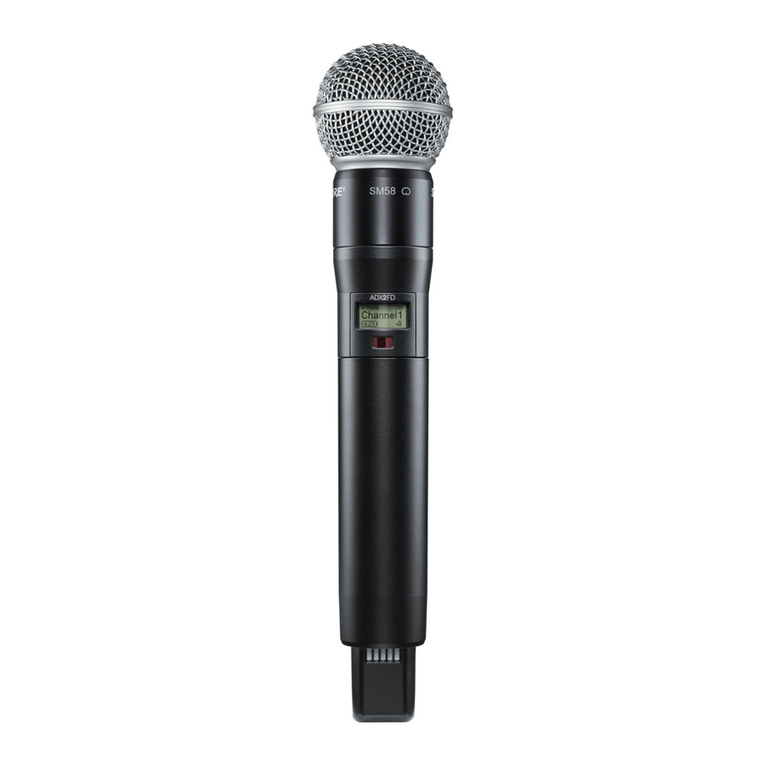
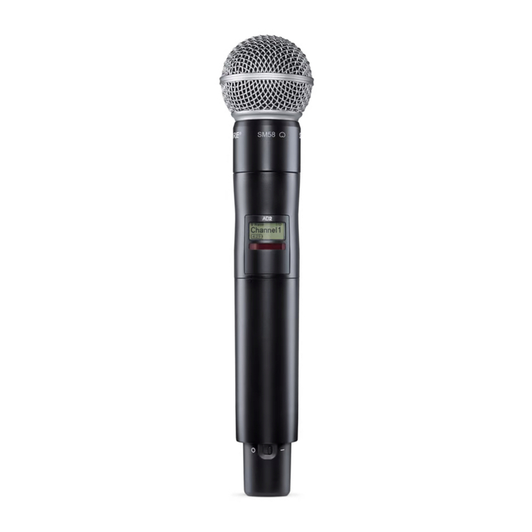
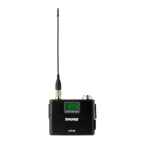
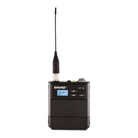
Shure T2 Vocal Artist Microphone Transmitter
4
Characteristics 25C1018 (CC)
The output power is +16.5 dBm (44.7 mW) into a 50 Ω load, at a fre-
quency of 169.4445 MHz. At the lowest acceptable battery voltage of
6 Vdc, the final collector current drops to 15 mAdc and the output power
to +13.9 dBm (24.4 mW).
Spurious Emissions: To minimize the production and radiation of
spurious emissions and harmonic energy, and to promote stable opera-
tion, the collector of each RF stage is separately decoupled from the 9 V
supply by ferrite chokes, resistors, and bypass capacitors. The base cir-
cuits are similarly decoupled except they use resistor-capacitor (R-C)
networks, whose higher-impedance levels are more appropriate.
RF Section: ETSI-Approved Models
Audio Input: Processed audio enters R201, an internal potentiom-
eter that is adjusted for 15 kHz deviation (100% modulation) when the
audio section provides a –2.2 dBV, 1 kHz tone.
Oscillation: The audio then goes to varactor diode D201, which is
part of the modulated oscillator-tripler stage (Q201). The latter’s base-
emitter circuit operates as a crystal-controlled Colpitts oscillator in the
20 MHz region. Fundamental-mode crystal Y201 is tuned 10 kHz below
series resonance by the series combination of frequency-netting coil
L201, diode D201, capacitor C203, and capacitor divider C206 and
C207.
Frequency and Temperature Stability: To ensure frequency sta-
bility despite changes in the battery voltage, regulated 5 Vdc bias is ap-
plied to the varactor diode and to the base of Q201. C203, C206, and
C207 provide temperature compensation.
Tuned Circuits (ETSI-Approved Models)
Stage 1: The collector circuit of Q201 is tuned to the third harmonic
of the oscillator frequency (approximately 60 MHz) by L202, C208, C244,
C210, L203, C214, C213, and C215. (The latter components also form a
capacitively tapped voltage divider for matching into the base of Q202.)
The output is double-tuned to provide high spectral purity. Regulated dc
bias is again employed to minimize changes in loading on the oscillator
stage and to stabilize the drive levels.
Stage 2: Q202 operates as a buffer, with the collector circuit tuned to
the output frequency (for example, 60 MHz). In this case, L204, C216,
C245, C218, L205, C222, C221, and C224 perform tuning and imped-
ance-matching functions. As in the preceding stage, regulated dc bias is
applied to the base circuit to stabilize the drive level, and the output is
double-tuned to provide spectral purity.
Stage 3: Q203 operates as a frequency tripler, with the collector cir-
cuit tuned to the output frequency (for example, 180 MHz). In this case,
L206, C226, C227, C229, L207, C230, and C232 perform tuning and
impedance-matching.
Stage 4: Q204 operates as a tuned amplifier. Resistive loading on
the input provides stability. The output circuit consists of a resonant tank
