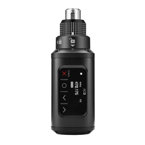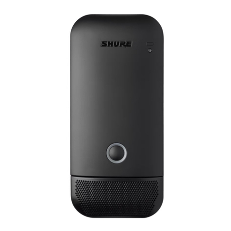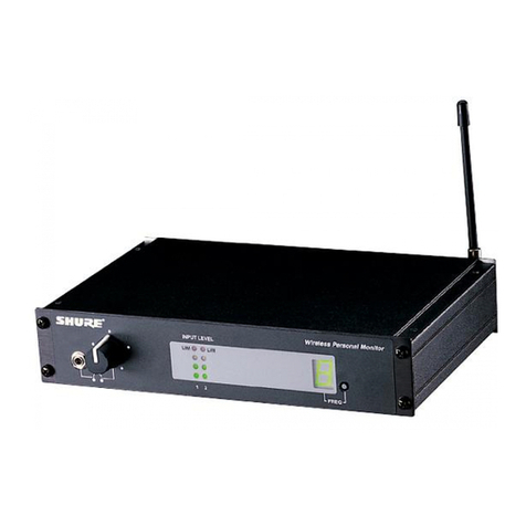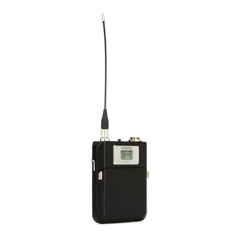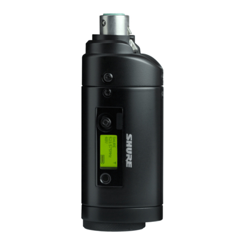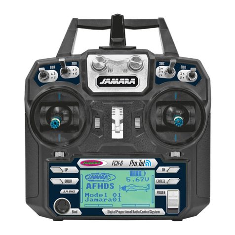
Shure UC1 Body-Pack UHF Transmitter
4 25A1043 (RI)
Characteristics
The audio is then fed to the tuning voltage pin of the voltage-
controlled oscillator (VCO) and modulates the carrier directly.
Using a phase-locked loop (PLL) frequency synthesized system
eliminates the need for multiplier stages and results in a much higher
degree of spectral purity. The VCO is shielded to prevent external rf
fields from affecting its operation.
Regulated 5 Vdc power is provided to ensure frequency stability with
changes in battery voltage.
The VCO can tune from 782 MHz to 810 MHz with a 1 Vdc to 4 Vdc
tuning voltage range; different VCOs are required for MB and KK frequen-
cy models. At the output of the VCO, the rf signal splits into two paths.
The output of the VCO is coupled by C134 to the frequency control
pin of the synthesizer, U104, pin 8. The internal circuitry of the synthe-
sizer divides the signal, as necessary, to the desired reference frequency
of 125 kHz. The synthesizer contains a reference oscillator circuit oper-
ating from a 4.0 MHz quartz crystal, Y101, that is adjusted by trimmer
C123. The transmitter output frequency is user-selectable in 125 kHz
increments, from 782 MHz to 806 MHz. Frequency range and increment
size vary for each model.
Frequency selection is made via microprocessor U101, which inter-
faces the user by means of the mode/select switches. The output of the
synthesizer is a series of pulses which are integrated by a passive loop
filter, R121, C130, R122, C129, C130, R123, and C132, to produce a
control voltage signal. The control voltage signal is then connected to
the VCO through amplifier U106A, which is used to isolate the PLL filter
from the audio modulation signals.
The VCO output is also coupled to an rf power amplifier through a
resistive pad consisting of R127, R128, R129, and R130. The signal is
then low-pass filtered through U107. The signal is coupled through C144.
Transistor Q102 acts as an rf pre-amplifier stage with typically 8 dB
of gain. R131, R132, and R133 provide dc bias to Q102. C145, C146,
C147, C149, C150, and L111 are used to decouple the rf off the emitter
of Q102, Vcc, and +9 Vdc supply voltages.
C152 couples the output of Q102 to low-pass filter U108. The signal
is then low-pass filtered through U108, and then coupled through C157.
Q104 acts as an rf amplifier stage with typically 16 dB of gain. L110,
R136, R137, and R138 provide dc bias to Q102. C160, C161, C162,
C163, C164, C165, and L114 are used to decouple the rf off the emitter
of Q104, Vcc, and +9 Vdc supply voltages.
L115 and C167 match the output of Q104 to low-pass filter U109.
The signal is coupled through C173 to the output antenna, W101.
The transmitter can deliver a maximum of +17 dBm (50 mW) to
the 50Ωantenna. During transmitter power-up and frequency selection,
the rf power is muted by bringing the gate of Q103 and Q105 high. The
RFUNMUTE signal is 5 Vdc. This provides approximately 45 dB rf attenu-
ation until the PLL has locked.
