ST STM32WB5MM-DK User manual

Introduction
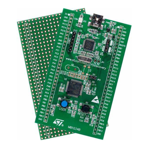
The STM32WB5MM-DK Discovery kit is designed as a complete demonstration and development platform for the
STMicroelectronics STM32W5MMG module based on the Arm® Cortex®-M4 and Arm® Cortex®-M0+ cores.
The STM32 device is a multi-protocol wireless and ultra-low-power device embedding a powerful and ultra-low-power radio
compliant with the Bluetooth® Low Energy (BLE) SIG specification v5.2 and with IEEE 802.15.4-2011.
The hardware features of the Discovery kits are available for users to develop their applications: Audio, USB, user buttons, and
Bluetooth® Low Energy. Extension connectors allow easy connection of an ARDUINO® board for a specific application.
An ST-LINK/V2-1 is integrated on the board, as an embedded in-circuit debugger and programmer for the STM32 MCU and the
USB Virtual COM port bridge.
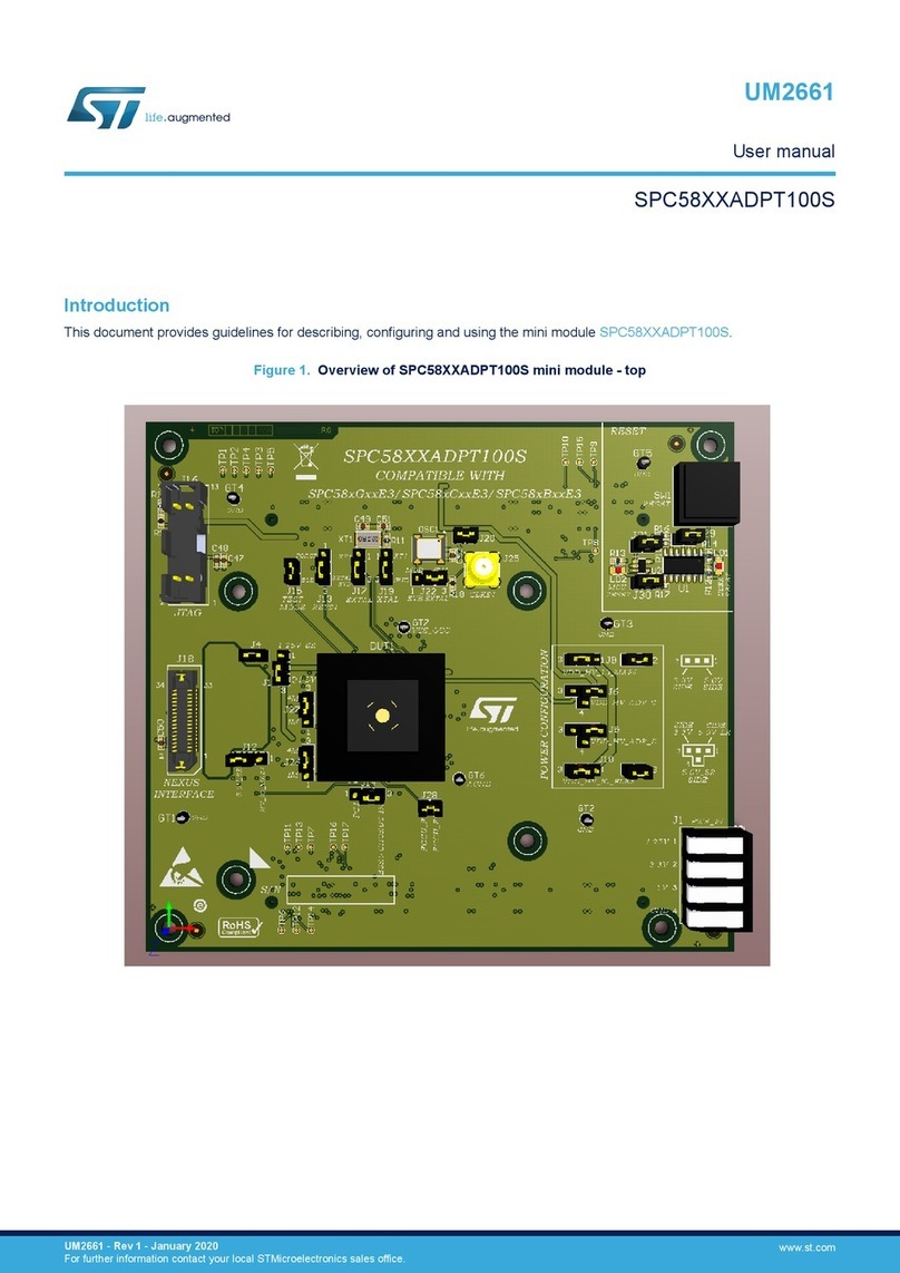
Figure 1. STM32WB5MM-DK Discovery kit
Picture is not contractual.
Discovery kit with STM32WB5MMG module
UM2825
User manual
UM2825 - Rev 1 - April 2021
For further information contact your local STMicroelectronics sales office. www.st.com

1Features
• STM32W5MMG (1-Mbyte Flash memory, 256-Kbyte SRAM, in Module RF package)
– Dual-core 32‑bit (Arm® Cortex®-M4 and dedicated M0+ CPU for real-time radio layer)
– 2.4 GHz RF transceiver supporting Bluetooth® specification V5.2, 802.15.4 with Zigbee®, Thread®, and
proprietary protocols
• 0.96-inch 128×64 OLED display
• 128-Mbit Quad-SPI NOR Flash Memory
• Temperature sensor
• Accelerometer/gyroscope sensor
• Time‑of‑Flight and gesture‑detection sensor
• Digital microphone
• RGB LED
• Infrared LED
• 3 push‑buttons (2 users and 1 reset) and 1 touch key button
• Board connectors:
– STMod+
–ARDUINO® Uno V3 expansion connector
– USB user with Micro-B connector
– TAG10 10-pin footprint
• Flexible power-supply options: ST-LINK/V2-1 USB connector, 5 V delivered by ARDUINO® or external
connector, USB charger, or USB power
• On-board ST-LINK/V2-1 debugger/programmer with USB re-enumeration capability: Virtual COM port and
debug port
• Comprehensive free software libraries and examples available with the STM32CubeWB MCU Package
• Support of a wide choice of Integrated Development Environments (IDEs) including IAR Embedded
Workbench®, MDK-ARM, and STM32CubeIDE
Note: Arm is a registered trademark of Arm Limited (or its subsidiaries) in the US and/or elsewhere.
UM2825
Features
UM2825 - Rev 1 page 2/42

2Ordering information
To order the STM32WB5MM-DK Discovery kit, refer to Table 1. Additional information is available from the
datasheet and reference manual of the target STM32.
Table 1. Ordering information
Order code Board reference Target STM32
STM32WB5MM-DK MB1292 STM32WB5MMGH6
2.1 Codification
The meaning of the codification is explained in Table 2.
Table 2. Codification explanation
STM32WBXXM-DK Description Example: STM32WB5MM-DK
STM32WB MCU series in STM32 32‑bit Arm Cortex MCUs STM32WB Series
XX MCU product line in the series STM32WBxM Modules line (5M module version)
DK Board type Discovery kit
UM2825
Ordering information
UM2825 - Rev 1 page 3/42

3Development environment
3.1 System requirements
• Windows® OS (7, 8, or 10), Linux® 64-bit, or macOS®
• USB Type-A or USB Type-C® to Micro-B cable
Note: macOS® is a trademark of Apple Inc. registered in the U.S. and other countries.
Linux® is a registered trademark of Linus Torvalds.
All other trademarks are the property of their respective owners.
3.2 Development toolchains
• IAR Systems® - IAR Embedded Workbench®(1)
• Keil® - MDK-ARM(1)
• STMicroelectronics - STM32CubeIDE
1. On Windows® only.
3.3 Demonstration software
The demonstration software, included in the STM32Cube MCU Package corresponding to the onboard
microcontroller, is preloaded in the STM32 Flash memory for easy demonstration of the device peripherals in
standalone mode. The latest versions of the demonstration source code and associated documentation can be
downloaded from www.st.com.
UM2825
Development environment
UM2825 - Rev 1 page 4/42

4Conventions
Table 3 provides the conventions used for the ON and OFF settings in the present document.
Table 3. ON/OFF convention
Convention Definition
Jumper JPx ON Jumper fitted
Jumper JPx OFF Jumper not fitted
Jumper JPx [1-2] Jumper fitted between Pin 1 and Pin 2
Solder bridge SBx ON SBx connections closed by 0 Ω resistor
Solder bridge SBx OFF SBx connections left open
Resistor Rx ON Resistor soldered
Resistor Rx OFF Resistor not soldered
UM2825
Conventions
UM2825 - Rev 1 page 5/42

5Safety recommendations
5.1 Targeted audience
This product target users with at least basic electronics or embedded software development knowledge like
engineer, technician, or student.
This board is not a toy and is not suited for use by children.
5.2 Handling the board
This product contains a bare printed circuit board and as with all product of this type, the user must be careful
about the following points:
• The connection pins on the board may be sharp, be careful when handling the board to avoid hurting
yourself.
• This board content static sensitive devices. To avoid damaging it, handle the board in an ESD‑proof
environment.
• While powered, do not touch the electric connections on the board with fingers or anything conductive. The
board operates at a voltage level that is not dangerous, but components may be damaged when shorted.
• Do not put any liquid on the board and avoid operating the board close to water or at a high humidity level.
• Do not operate the board if dirty or dusty.
UM2825
Safety recommendations
UM2825 - Rev 1 page 6/42

6Quick start
This section describes how to quickly start development using the STM32WB5MM-DK Discovery kit.
To use the product, the user must accept the Evaluation Product License Agreement from the www.st.com/epla
webpage.
Before the first use, make sure that no damage occurred to the board during shipment:
• All socketed components are firmly secured in their sockets.
• No component is loose in the board blister.
The Discovery kit is an easy-to-use Discovery kit to quickly evaluate and start development with an STM32
microcontroller in an RF module package.
6.1 Getting started
1. Check jumper positions on board: JP1 and JP5 ON, JP2 (Power source) on USB MCU.
2. Install ST BLE Sensor Mobile Application on a BLE compatible mobile device from App Store or Google
Play.
3. On the host PC any freeware or commercial audio recording software can be used to interface with the
Discovery board. For example, Audacity® is an open‑source, cross-platform program for recording and
audio editing, available from https://www.audacityteam.org/download.
4. Connect the Discovery board to a PC with a USB cable Type-A to Micro-B through USB connector CN6
(USB USER). The board will be automatically recognized by Windows as a standard microphone (Found in
“Windows device manager” as STM32 AUDIO Streaming in FS Mode). As soon as BLE Advertising appears
on Discovery display, the board is ready to connect.
5. Use ST BLE sensor mobile application to detect the STM32WB5MM-DK (BVL-WB1) with ST Bluetooth®
00:80:E1:26:XX:XX device address and connect to it. The text BLE Connected appears on the Discovery
board display, while the BlueVoice FullDuplex page is shown on the mobile application.
6. Pushing the B1 button on the board starts the audio acquisition and streaming from the Discovery on the
application (Audio TX on the display), audio can be heard from the smartphone speaker.
7. Enabling the Start switch on the App starts audio streaming from the Smartphone to the Discovery (Audio
RX on the display). Open Audacity on the host PC. To start an audio recording, check first if the audio input
device is STM32 AUDIO streaming and then press the recording button. To listen to the received audio while
recording, go to EditPreferencesRecording and check Software playthrough of input.
8. A full-duplex communication is performed if the streaming is enabled on both sides, “Full-duplex” message
appears on Discovery display.
9. For more details refer to the user manual Getting started with the STM32Cube function pack for STM32WB
MCU featuring advanced audio streaming over Bluetooth 5.0 using Opus codec (UM2614) of FP-AUD-
BVLINKWB1, together with the demonstration software version v.2.0.0 or higher.
UM2825
Quick start
UM2825 - Rev 1 page 7/42
7Hardware layout and configuration
The STM32WB5MM-DK Discovery kit is designed around the STM32W5MMG RF module that includes an
STM32WB55VG Bluetooth® Low Energy microcontroller, a ceramic antenna, two crystals, and peripheral
components. The hardware block diagram, shown in Figure 2, illustrates the connections between the
STM32W5MMG RF module and the peripheral components (Quad-SPI Flash memory, OLED display, USB OTG
HS and FS connectors, USART, audio, ARDUINO® Uno V3, STMod+ shields, and embedded ST-LINK). Figure 3
and Figure 4 show the location of the main components on both sides of the Discovery board. Figure 5 shows the
STM32WB5MM-DK board mechanical dimensions.
Figure 2. STM32WB5MM-DK hardware block diagram
UM2825
Hardware layout and configuration
UM2825 - Rev 1 page 8/42

Figure 3. STM32WB5MM-DK PCB layout (top view)
Figure 4. STM32WB5MM-DK PCB layout (bottom view)
UM2825
Hardware layout and configuration
UM2825 - Rev 1 page 9/42

Figure 5. STM32WB5MM-DK board mechanical dimensions (top view, in millimeters)
UM2825
Hardware layout and configuration
UM2825 - Rev 1 page 10/42

7.1 Embedded ST-LINK/V2-1
The ST-LINK/V2-1 programming and debugging tool is integrated into the STM32WB5MM-DK Discovery kit. For
information about debugging and programming features refer to ST-LINK/V2 in-circuit debugger/programmer for
STM8 and STM32 user manual (UM1075), which describes in detail all the ST-LINK/V2 features.
The additional features supported on the ST-LINK/V2-1 are:
• USB software re-enumeration
• Virtual COM port interface on USB
• Mass storage interface on USB
• USB power management request for more than 100 mA power on USB (limited to 300 mA for this board)
The following features are no more supported on the ST-LINK/V2-1:
• Application voltage lower than 3 V
7.1.1 Drivers
The ST-LINK/V2-1 requires a dedicated USB driver, which, for Windows 7®and Windows 8®, is found at
www.st.com. For Windows 10®, it is not necessary to install the driver, as the ST-LINK is automatically identified.
In case the STM32WB5MM-DK Discovery kit is connected to the PC before the driver is installed, some
Discovery board interfaces may be declared as “Unknown” in the PC device manager. In this case, the user
must install the dedicated driver files, and update the driver of the connected device from the device manager as
shown in Figure 6.
Note: Prefer using the “USB Composite Device” handle for a full recovery.
Figure 6. USB composite device
7.1.2 ST-LINK/V2-1 firmware upgrade
The ST-LINK/V2-1 embeds a firmware upgrade mechanism for the in-situ upgrade through the USB port. As the
firmware may evolve during the lifetime of the ST-LINK/V2-1 product (for example new functionalities, bug fixes,
support for new microcontroller families), it is recommended to visit the www.st.com website before starting to use
the STM32WB5MM-DK Discovery kit and periodically, to stay up-to-date with the latest firmware version.
UM2825
Embedded ST-LINK/V2-1
UM2825 - Rev 1 page 11/42

7.2 Power supply
7.2.1 General description
The STM32W5MMG module embedded on this STM32WB5MM-DK Discovery kit is always supplied by 3V3
but the board proposes a lot of possibilities to supply the module. The supply source can come from USB or
ARDUINO® connectors, or from an external power supply. Figure 7 describes the board power tree. Moreover,
this figure also shows the default state of the jumpers and solder bridges.
Figure 7. STM32WB5MM-DK power tree
7.2.2 7 to 12 V power supply
The STM32WB5MM-DK Discovery kit can be powered with a 7 to 12 V DC power source. There are two
accesses for this type of levels:
• VIN pin of the CN2-8 ARDUINO® connector. It is possible to apply until +12 V on this pin or use an
ARDUINO® shield which can deliver this type of voltage on the VIN pin.
• Ext input (CN8).
Caution: In this case, paying attention to the configuration of the jumpers and solder bridges is very important. Verify this
configuration on Table 4.
These two sources are connected to a linear low drop voltage regulator (U9). The 5 V output of this regulator is a
potential source of the 5V signal. Refer to Section 7.2.3 for the details.
UM2825
Power supply
UM2825 - Rev 1 page 12/42

7.2.3 5 V power supply
The STM32WB5MM-DK Discovery kit can be powered by a 5 V DC power source. The 5V signal can come from
several connectors:
• 5V_USB_STLK connected to CN11 (default configuration for the supply of the board). This connector is
dedicated to access to the STLINK/V2 and Virtual COM port and can supply power from the host computer.
It is also possible to connect a USB charger to this connector. In this case, the ST-LINK and the Virtual COM
port cannot be accessible.
• 5V_USB_MCU connected to User USB. This USB port is directly connected to the STM32W5MMG as a
USB port. The same remark applies as for 5V_USB-STLK, the supply can be provided by the host computer
or by USB charger.
• Ext input (CN8). Be careful, in this case, the state of the jumpers and the solder bridges is very important.
Refer to Section 7.2.2 for details.
• 7-12V input through the U9 voltage regulator. Refer to Section 7.2.2 for details.
The JP2 jumper JP2 selects the 5V source. Table 4 shows the configuration for the selected source.
Caution: Depending on the current needed on the devices connected to the USB port, and the board itself, power
limitations can prevent the system from working as expected. The user must ensure that the STM32WB5MM-DK
Discovery kit is supplied with an adequate power source depending on the needed current.
Table 4. JP2 power supply selector description
Jumper/solder bridge Setting Configuration(1)
JP2
5V supply
source selector
STM32WB5MM-DK is supplied through the
CN11 Micro-B USB receptacle (USB_STLINK).
STM32WB5MM-DK is supplied through CN6
Micro-B receptacle (USB_USER).
STM32WB5MM-DK is supplied through pin 8
of CN2 (ARDUINO®) or CN8 (Refer to the
configuration details on the present power supply
section).
STM32WB5MM-DK is supplied through CN8
directly (Refer to the configuration details on the
present power supply section).
1. The default configuration is in bold
When 5V_USB_STLINK is used and JP2 [1-2] ON, the sequence is specific. In the beginning, only STM32F103 is
supplied. If the USB enumeration succeeds, the 5V_USB_STLINK power is enabled by asserting the PWR_ENn
signal from STM32F103CBT6. This pin is connected to an STMPS2141STR power switch which supplies the rest
of the board. This power switch also features a current limitation to protect the PC in case of currents exceeding
300 mA.
UM2825
Power supply
UM2825 - Rev 1 page 13/42

7.2.4 Current measurement
As the device handles low‑power features, it may be worth measuring the current consumed by the
STM32W5MMG module. To easily perform this measurement, there are two possibilities:
1. Measure the supply current of the STM32W5MMG module using an ammeter in place of the JP1 jumper. In
this case, all supply sources can be used except the AVDD coming from the ARDUINO® connector. Figure 8
shows the configuration:
Figure 8. Current measurement with an ammeter
2. Or use an external power supply with current measurements capability. In this case, the JP1 jumper must be
removed, and the supply must be connected to pin 2 of JP1, as shown in Figure 9. The supply voltage must
be 3.3 V and AVDD input (CN1-8) must not be used during this measurement.
Figure 9. Current measurement with an external power supply
UM2825
Power supply
UM2825 - Rev 1 page 14/42

7.3 Clock sources
7.3.1 HSE clock reference
The high-speed clock (HSE) of the STM32WB5MM-DK Discovery kit is embedded on the STM32W5MMG
module. It uses a 32 MHz crystal oscillator. The HSE oscillator is trimmed during module manufacturing.
7.3.2 LSE clock reference
The low‑speed clock (LSE) of the STM32WB5MM-DK Discovery kit is embedded on the STM32W5MMG module.
It uses a 32.768 kHz crystal oscillator.
7.4 Reset sources
The reset signal of STM32W5MMG is active LOW. The internal pull-up resistor forces the RST signal to a HIGH
level.
The sources of reset are the following:
• B3 push‑button reset (small black button)
• Embedded ST-LINK/V2-1
• Pin 3 of the CN2 ARDUINO® connector, reset from the ARDUINO® board
• Pin 10 of the CN7 TAG-Connect (TAG10) connector
UM2825
Clock sources
UM2825 - Rev 1 page 15/42

7.5 Board functions
7.5.1 128 × 64‑pixel OLED display
The STM32WB5MM-DK board embeds the 9OL9935718000 OLED display from RiTdisplay Corporation. It is a
128 × 64‑pixel OLED display panel matrix, with high contrast and SPI driven interface to display messages and
user menus. The OLED panel matrix is controlled by an SSD1315Z embedded inside the display.
7.5.2 U8 Quad-SPI NOR Flash memory
The STM32WB5MM-DK board embeds a 128‑Mbit Quad-SPI NOR Flash memory device
(S25FL128SDSMFV001 from Cypress), which is connected to an STM32W5MMG dedicated Quad-SPI interface
described in Table 5.
Table 5. U8 Quad-SPI NOR Flash memory connection with STM32W5MMG
Quad-SPI memory pin
number
Quad-SPI memory pin
name STM32W5MMG pin number STM32W5MMG signal name
7 /CS 70 (PD3) QSPI_BK_NCS
16 SCK 56 (PA3) QSPI_BK_SCK
15 IO0 11 (PB9) QSPI_BK_IO0
8 IO1 80 (PD5) QSPI_BK_IO1
9 IO2 81 (PD6) QSPI_BK_IO2
1 IO3 67 (PD7) QSPI_BK_IO3
7.5.3 Virtual COM port
ST-LINK/V2-1 offers a USB Virtual COM port bridge. This feature allows access to the STM32W5MMG USART1
by the CN11 USB_STLINK connector.
By default, this STM32W5MMG USART1 interface is connected to the UART2 port of the STM32F103 ST-LINK/
V2-1 MCU.
Table 6. UART interface pinout description
STM32W5MMG CN10 STM32F103
USART1 RX (PB7/pin 18) Pin 1 STLINK_TX: UART2 TX (PA2/pin 12)
USART1 TX (PB6/pin 39) Pin 2 STLINK_RX: UART2 RX (PA3/pin 13)
7.5.4 MEMS microphone
The IMP34DT05TR MEMs microphone is connected through an SAI interface to the STM32W5MMG module.
SAI1_CK2 and SAI1_DI2 are connected to the microphone and ensure the recording.
Table 7. IMP34DT05TR‑STM32W5MMG SAI interface
STM32W5MMG IMP34DT05TR
SAI1_CK2 (PA8/pin 50) CLK, Clock in (pin 3)
SAI1_DI2 (PA9/pin 51) DOUT, PDM data out (pin 4)
UM2825
Board functions
UM2825 - Rev 1 page 16/42

7.5.5 LEDs
Description
Five LEDs on the top side of the STM32WB5MM-DK board help the user during the application development.
Figure 10. LEDs location
• LD1: this red LED indicates that the current distribution could not be performed as expected.
• LD2: this LED turns green when the 5 V is available. Refer to Section 7.2.3 to select the 5 V source.
• LD3 COM: LD3 is a bi-color LED, which default status is red, turns to green to indicate that communication is
in progress between the PC and the ST-LINK/V2-1, as follows:
– Slow blinking red/OFF: at power-on, before USB initialization
– Fast blinking red/OFF: after the first correct communication between PC and ST-LINK/V2-1
(enumeration)
– Red ON: when initialization between PC and ST-LINK/V2-1 is successfully finished
– Green ON: after successful target communication initialization
– Blinking red/green: during communication with the target
– Green ON: communication finished and OK
– Orange ON: communication failure
• LD4: this LED is an RGB LED. It is available for the user application.
• LDIR1: this LED allows to transmit infrared radiation signal.
RGB LED
The resources coming from STM32W5MMG are shared between the RGB and IR LEDs. It is not possible to use
them simultaneously. The selection is done by JP4 and JP5 jumpers.
To use the RGB LED, JP5 must be ON and JP4 OFF. In this configuration, GPIO_SELECT2 (PH1) is the chip
select for this RGB device on SPI1.
The RGB LED is driven by the TLC59731 PWM LED driver from Texas Instruments.
UM2825
Board functions
UM2825 - Rev 1 page 17/42
Infrared (IR) LED
The resources coming from STM32W5MMG are shared between the RGB and IR LEDs. It is not possible to use
them simultaneously. The selection is done by JP4 and JP5 jumpers.
To use the IR LED, JP4 must be ON and JP5 OFF. In this configuration, GPIO_SELECT2 (PH1) is the chip select
for this IR transmission. PB9 is in charge of the IR modulation. This GPIO is shared with the Quad-SPI Flash
Memory. It is possible to use the Flash Memory and IR LED on the same application but not exactly at the same
time.
The IR LED is driven by TIM16 and TIM17 internal timers. The schematic proposal does not use the IR_OUT
feature. A firmware example is available on the firmware package.
7.5.6 Push-buttons
Description
The STM32WB5MM-DK Discovery kit provides three buttons:
• B1 user push‑button
• B2 user push‑button
• B3 reset push‑button, used to reset STM32WB5MM-DK Discovery kit.
Reset push‑button
B3 is a small push‑button dedicated to the hardware reset of the STM32WB5MM-DK. It is separated from the
other push‑buttons to avoid mishandling.
User push‑buttons
There are two push‑buttons available for the user application. They are connected to PC12 and PC13. It is
possible to use them for GPIO reading or to wake up the device.
Table 8. Physical user interface I/O configuration (push‑buttons)
Name I/O Available wake-up
B1 user1 push‑button PC12 WKUP3
B2 user2 push‑button PC13 WKUP2
7.5.7 Touch sensor
The STM32WB5MM-DK board embeds a touch sensor. The touch sensor is working with the charge and
discharge of a capacitor. Touching the round panel with a finger charges a capacitor. Once the capacitor is
charged at VDD, the charge is transferred to another capacitor, called the sampling capacitor.
Two groups of I/Os are connected to use it:
Table 9. Physical user interface I/O configuration (touch sensor)
I/O group I/O Configuration
Shield group 4 PC6 TSC_G4_IO1
PC7 TSC_G4_IO2
Touch key group 6 PD10 TSC_G6_IO1
PD11 TSC_G6_IO2
UM2825
Board functions
UM2825 - Rev 1 page 18/42
7.6 Embedded sensors
7.6.1 I2C interface
The STM32WB5MM-DK embedded sensors are connected to the STM32W5MMG module with an I2C bus. The
Time‑of‑Flight (ToF), accelerometer/gyroscope, and temperature sensors are connected to STM32W5MMG I2C3
bus.
Table 10. STM32W5MMG I2C
STM32W5MMG port Description
PB13 (pin 35) I2C3_SCL
PB11 (pin 46) I2C3_SDA
The address is a 7-bits address with an additional R/W bit (HIGH for reading, LOW for writing). describes the
different address to R/W action for each component:
Table 11. Sensor I2C addresses
Device Action Address
ISM330DHCX
(Accelerometer/gyroscope sensor)
Read 0b11010111 (D7h)
Write 0b11010110 (D6h)
STTS22H
(Temperature sensor)
Read 0b01110001 (71h)
Write 0b01110000 (70h)
VL53L0CXV0DH/1
(Time‑of‑Flight sensor)
Read 0b01010011 (53h)
Write 0b01010010 (52h)
UM2825
Embedded sensors
UM2825 - Rev 1 page 19/42
7.6.2 U6 Time‑of‑Flight (ToF) sensor
U6 VL53L0CXV0DH/1 is a device that allows measuring the Time‑of‑Flight (ToF) of a laser beam. It is connected
to the STM32W5MMG through the I2C interface.
This sensor can make a distance measurement and obstacle detection until two meters, and 1D‑gesture
recognition.
Figure 11. Direction, angle, and side operating
VL53L0CXV0DH/1 contains a laser emitter and the corresponding drive circuitry. The laser output is designed
to remain within Class 1 laser safety limits under all reasonably foreseeable conditions including single faults
in compliance with IEC 60825-1:2014 (third edition). The laser output remains within Class 1 limits as long as
the STMicroelectronics recommended device settings are used and the operating conditions specified in the
STM32WB datasheets are respected. The laser output power must not be increased by any means and no optics
used to focus the laser beam. Figure 12 shows the warning label for Class 1 laser products.
Figure 12. Class 1 laser product label
Table 12. U6 Time‑of‑Flight sensor I2C address
Device Action Address
VL53L0CXV0DH/1 Read 0b01010011 (53h)
Write 0b01010010 (52h)
UM2825
Embedded sensors
UM2825 - Rev 1 page 20/42
Table of contents
Other ST Control Unit manuals
Popular Control Unit manuals by other brands

Axis
Axis 2191 installation guide

LEGRAND
LEGRAND AU7004 installation instructions

PDi
PDi PD251-047 quick start guide

National Instruments
National Instruments PXIe-8267 Getting started guide

Roving Networks
Roving Networks RN-174 manual

ZURN
ZURN AquaSense ZER-W2 Series Installation, operation, maintenance and parts manual