ST Teseo-LIV3F User manual

February 2019 UM2231 Rev 6 1/26
1
UM2231
User manual
Teseo-LIV3 GNSS Modules - Hardware Manual
Introduction
Teseo-LIV3 is a family of tiny GNSS modules sized 9.7 mm × 10.1 mm × 2.5 mm featuring
STMicroelectronics®positioning receiver Teseo III. It is a standalone positioning receiver
which embeds the new ST GNSS positioning engine capable of receiving signals from
multiple satellite navigation systems.
This document is relevant for the following Teseo-LIV3 modules.
In Figure 1 pinout of the module is represented as follows:
Figure 1. Teseo-LIV3 pinout
Table 1. Teseo-LIV3 supported devices
Device type Description
Teseo-LIV3F Tiny GNSS module flash based
Teseo-LIV3R Tiny GNSS module ROM based
www.st.com

Contents UM2231
2/26 UM2231 Rev 6
Contents
1 Power . . . . . . . . . . . . . . . . . . . . . . . . . . . . . . . . . . . . . . . . . . . . . . . . . . . . . 6
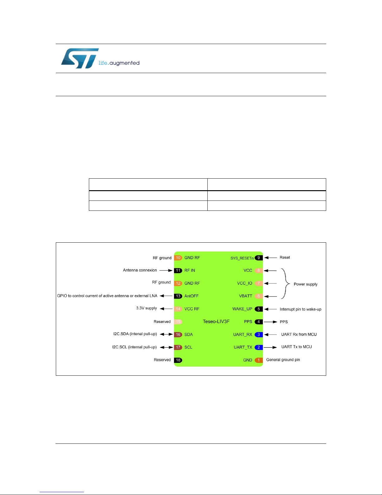
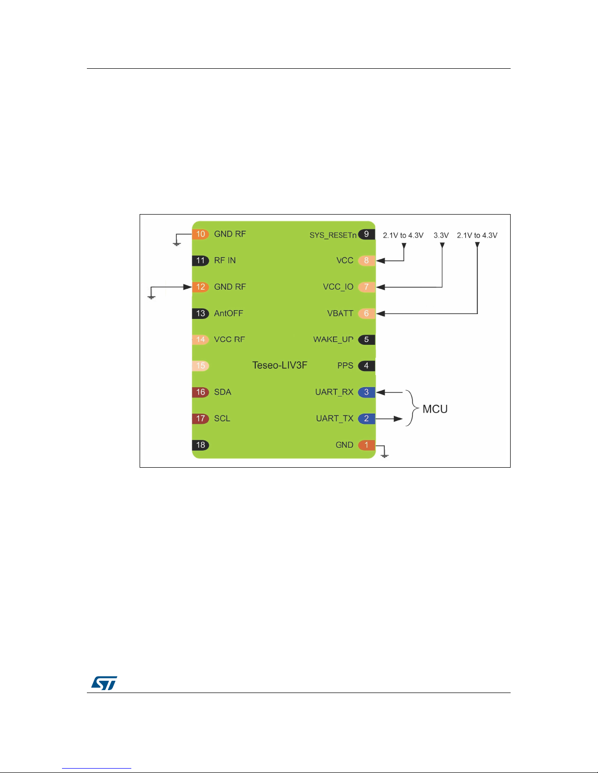
1.1 VCC (pin8) . . . . . . . . . . . . . . . . . . . . . . . . . . . . . . . . . . . . . . . . . . . . . . . . . 6
1.2 VBAT (pin6) . . . . . . . . . . . . . . . . . . . . . . . . . . . . . . . . . . . . . . . . . . . . . . . . 6
1.3 VCC_IO (pin7) . . . . . . . . . . . . . . . . . . . . . . . . . . . . . . . . . . . . . . . . . . . . . . 7
1.4 VCC_RF (pin14) . . . . . . . . . . . . . . . . . . . . . . . . . . . . . . . . . . . . . . . . . . . . . 7
1.5 Power supply design reference . . . . . . . . . . . . . . . . . . . . . . . . . . . . . . . . . 8
1.6 Current consumption optimization . . . . . . . . . . . . . . . . . . . . . . . . . . . . . . . 8
2 Reserved (pin15, 18) . . . . . . . . . . . . . . . . . . . . . . . . . . . . . . . . . . . . . . . . 10
3 Interfaces . . . . . . . . . . . . . . . . . . . . . . . . . . . . . . . . . . . . . . . . . . . . . . . . . 11
3.1 I2C (pin16, 17) . . . . . . . . . . . . . . . . . . . . . . . . . . . . . . . . . . . . . . . . . . . . . .11
3.2 UART (pin2, 3) . . . . . . . . . . . . . . . . . . . . . . . . . . . . . . . . . . . . . . . . . . . . . .11
4 I/O pins . . . . . . . . . . . . . . . . . . . . . . . . . . . . . . . . . . . . . . . . . . . . . . . . . . . 12
4.1 PPS (pin4) . . . . . . . . . . . . . . . . . . . . . . . . . . . . . . . . . . . . . . . . . . . . . . . . 12
4.2 Wake_Up (pin5) . . . . . . . . . . . . . . . . . . . . . . . . . . . . . . . . . . . . . . . . . . . . 12
4.3 SYS_RESETn (pin9) . . . . . . . . . . . . . . . . . . . . . . . . . . . . . . . . . . . . . . . . 12
4.4 RF_IN (pin10) . . . . . . . . . . . . . . . . . . . . . . . . . . . . . . . . . . . . . . . . . . . . . . 12
4.5 AntOFF (pin13) . . . . . . . . . . . . . . . . . . . . . . . . . . . . . . . . . . . . . . . . . . . . . 12
5 Standby modes . . . . . . . . . . . . . . . . . . . . . . . . . . . . . . . . . . . . . . . . . . . . 13
5.1 Software standby . . . . . . . . . . . . . . . . . . . . . . . . . . . . . . . . . . . . . . . . . . . 13
5.2 Hardware standby . . . . . . . . . . . . . . . . . . . . . . . . . . . . . . . . . . . . . . . . . . 13
6 Front ends management . . . . . . . . . . . . . . . . . . . . . . . . . . . . . . . . . . . . . 14
6.1 External LNA . . . . . . . . . . . . . . . . . . . . . . . . . . . . . . . . . . . . . . . . . . . . . . 14
6.2 Active antenna . . . . . . . . . . . . . . . . . . . . . . . . . . . . . . . . . . . . . . . . . . . . . 15
7 Reference schematic and BOM . . . . . . . . . . . . . . . . . . . . . . . . . . . . . . . 16
7.1 Schematic . . . . . . . . . . . . . . . . . . . . . . . . . . . . . . . . . . . . . . . . . . . . . . . . . 16
7.1.1 Bill of material . . . . . . . . . . . . . . . . . . . . . . . . . . . . . . . . . . . . . . . . . . . . 17

UM2231 Rev 6 3/26
UM2231 Contents
3
8 Layout recommendation . . . . . . . . . . . . . . . . . . . . . . . . . . . . . . . . . . . . . 19
9 Antenna recommendations . . . . . . . . . . . . . . . . . . . . . . . . . . . . . . . . . . 21
9.1 Patch antennas . . . . . . . . . . . . . . . . . . . . . . . . . . . . . . . . . . . . . . . . . . . . 21
9.1.1 Antenna on the opposite side . . . . . . . . . . . . . . . . . . . . . . . . . . . . . . . . 21
9.1.2 Antenna on the same side than Teseo-LIV3 . . . . . . . . . . . . . . . . . . . . . 22
9.2 Chip antenna . . . . . . . . . . . . . . . . . . . . . . . . . . . . . . . . . . . . . . . . . . . . . . 23
9.3 Remote antenna . . . . . . . . . . . . . . . . . . . . . . . . . . . . . . . . . . . . . . . . . . . . 24
10 Revision history . . . . . . . . . . . . . . . . . . . . . . . . . . . . . . . . . . . . . . . . . . . 25

List of tables UM2231
4/26 UM2231 Rev 6
List of tables
Table 1. Teseo-LIV3 supported devices . . . . . . . . . . . . . . . . . . . . . . . . . . . . . . . . . . . . . . . . . . . . . . . 1
Table 2. Bill of material . . . . . . . . . . . . . . . . . . . . . . . . . . . . . . . . . . . . . . . . . . . . . . . . . . . . . . . . . . . 17
Table 3. List of suggested antennas . . . . . . . . . . . . . . . . . . . . . . . . . . . . . . . . . . . . . . . . . . . . . . . . . 21
Table 4. List of SMD antennas . . . . . . . . . . . . . . . . . . . . . . . . . . . . . . . . . . . . . . . . . . . . . . . . . . . . . 23
Table 5. Document revision history . . . . . . . . . . . . . . . . . . . . . . . . . . . . . . . . . . . . . . . . . . . . . . . . . 25

UM2231 Rev 6 5/26
UM2231 List of figures
5
List of figures
Figure 1. Teseo-LIV3 pinout . . . . . . . . . . . . . . . . . . . . . . . . . . . . . . . . . . . . . . . . . . . . . . . . . . . . . . . . 1
Figure 2. Inductor on VCC power line . . . . . . . . . . . . . . . . . . . . . . . . . . . . . . . . . . . . . . . . . . . . . . . . . 6
Figure 3. Teseo-LIV3 minimum connection . . . . . . . . . . . . . . . . . . . . . . . . . . . . . . . . . . . . . . . . . . . . . 7
Figure 4. Output supply filtering . . . . . . . . . . . . . . . . . . . . . . . . . . . . . . . . . . . . . . . . . . . . . . . . . . . . . . 8
Figure 5. Power supply filtering . . . . . . . . . . . . . . . . . . . . . . . . . . . . . . . . . . . . . . . . . . . . . . . . . . . . . . 8
Figure 6. Example of SMPS to improve current consumption . . . . . . . . . . . . . . . . . . . . . . . . . . . . . . . 9
Figure 7. UART filtering . . . . . . . . . . . . . . . . . . . . . . . . . . . . . . . . . . . . . . . . . . . . . . . . . . . . . . . . . . . 11
Figure 8. PPS pin filtering . . . . . . . . . . . . . . . . . . . . . . . . . . . . . . . . . . . . . . . . . . . . . . . . . . . . . . . . . 12
Figure 9. External LNA control. . . . . . . . . . . . . . . . . . . . . . . . . . . . . . . . . . . . . . . . . . . . . . . . . . . . . . 14
Figure 10. Active antenna current switch control . . . . . . . . . . . . . . . . . . . . . . . . . . . . . . . . . . . . . . . . . 15
Figure 11. Active antenna current sense . . . . . . . . . . . . . . . . . . . . . . . . . . . . . . . . . . . . . . . . . . . . . . . 15
Figure 12. General schematic . . . . . . . . . . . . . . . . . . . . . . . . . . . . . . . . . . . . . . . . . . . . . . . . . . . . . . . 16
Figure 13. Placing parallel component pads on 50 ohms line . . . . . . . . . . . . . . . . . . . . . . . . . . . . . . . 19
Figure 14. Reuse pads of one component on the line bypassing . . . . . . . . . . . . . . . . . . . . . . . . . . . . 19
Figure 15. Layout proposal . . . . . . . . . . . . . . . . . . . . . . . . . . . . . . . . . . . . . . . . . . . . . . . . . . . . . . . . . 20
Figure 16. Pin1 gnd “isolation” example . . . . . . . . . . . . . . . . . . . . . . . . . . . . . . . . . . . . . . . . . . . . . . . 20
Figure 17. Antenna vs Teseo-LIV3 placement. . . . . . . . . . . . . . . . . . . . . . . . . . . . . . . . . . . . . . . . . . . 21
Figure 18. Antenna on bottom layer and Teseo-LIV3 on top layout example . . . . . . . . . . . . . . . . . . . 22
Figure 19. 25×25mm SMD Antenna and Teseo-LIV3 on same layer example . . . . . . . . . . . . . . . . . . 23
Figure 20. Chip Antenna and Teseo-LIV3 on same layer example . . . . . . . . . . . . . . . . . . . . . . . . . . . 24

Power UM2231
6/26 UM2231 Rev 6
1 Power
Teseo-LIV3 is supplied by 3 power pins: VCC (pin8), VCC_IO (pin7) and VBAT (pin6).
1.1 VCC (pin8)
VCC is the main supply. VCC limiting values are: 2.1 V - 4.3 V.
At startup or during low power application current can change suddenly. It is important that
supply IC is able to provide this current variation.
Take care that interference on VCC power line could degrade Teseo-LIV3 sensitivity
performance, to avoid that it’s recommended a 27 nH inductor (Murata LQG15HS27NJ02)
as shown in Figure 2: Inductor on VCC power line.
Figure 2. Inductor on VCC power line
The suggested inductor on the VCC power line is able to recover interference coming from
VCC power line.
1.2 VBAT (pin6)
VBAT is the supply for the low power domain backup: backup RAM and RTC.
VBAT can be either connected to VCC or it can be supplied by a dedicated supply always
ON. When VBAT supply is kept ON during low power mode to allow fast recovery of GNSS

UM2231 Rev 6 7/26
UM2231 Power
24
fix VBAT prevents current flow as soon as VBAT is lower than VCC. It is important when
VBAT is supplied with small battery and especially if battery is not rechargeable.
VBAT range can be from 2.1 V to 4.3 V.
1.3 VCC_IO (pin7)
VCC_IO is 3.3 V.
Figure 3 shows the minimum connection to make Teseo-LIV3 GNSS working.
Figure 3. Teseo-LIV3 minimum connection
1.4 VCC_RF (pin14)
VCC_RF is an output image of VCC with a filtering for LNA or active antenna supply.
It can be filtered to remove high frequency noise as shown in Figure 4.

Power UM2231
8/26 UM2231 Rev 6
Figure 4. Output supply filtering
1.5 Power supply design reference
During prototyping stage, for the first PCBs, it is recommended to plan to have some filtering
components on Teseo-LIV3 power supplies as shown In Figure 5.
Figure 5. Power supply filtering
Inductor size is 0401 (1.0×0.5mm) and capacitors are 0201 (0.6×0.3mm).
In case VCC_IO is separate from VCC, a serial 27nH inductor could also be planned for first
PCBs.
If all 3 pins have common supply, one single capacitor and one single inductor can be used.
If not it is recommended to duplicate the filtering.
1.6 Current consumption optimization
Use of an SMPS at 2.1 V to supply VCC is recommended to optimize current consumption.
Here is an application example with ST1S12GR with an efficiency around 85%.

UM2231 Rev 6 9/26
UM2231 Power
24
Figure 6. Example of SMPS to improve current consumption
If VCC_IO is also supplied by an SMPS, this will reach the lowest current consumption.

Reserved (pin15, 18) UM2231
10/26 UM2231 Rev 6
2 Reserved (pin15, 18)
In Teseo-LIV3 pin15 and 18 are reserved.

UM2231 Rev 6 11/26
UM2231 Interfaces
24
3 Interfaces
3.1 I2C (pin16, 17)
Teseo-LIV3 supports I2C slave mode only.
Internal 10 Kpull-up resistor on VCC_IO is present. It is important to avoid having other
pull-up for current leakage in low power mode.
3.2 UART (pin2, 3)
UART is a Universal Asynchronous Receiver/Transmitter that supports much of the
functionality of the industry-standard 16C650 UART.
These UARTs vary from industry-standard 16C650 on some minor points which are:
Receive FIFO trigger levels
The deltas of the modem status signals are not available
1.5 stop bit is not supported
Independent receive clock feature is not supported
During prototyping stage, for the first PCBs, it is recommended to plan to have some filtering
components on Teseo-LIV3 UART lines as shown in Figure 7.
Figure 7. UART filtering

I/O pins UM2231
12/26 UM2231 Rev 6
4 I/O pins
4.1 PPS (pin4)
PPS is the time pulse every one second. It can be configured with different condition of
pulses.
During prototyping stage, for the first PCBs, it is recommended to plan to have some filtering
components on Teseo-LIV3 PPS pin as shown in Figure 8.
Figure 8. PPS pin filtering
4.2 Wake_Up (pin5)
It is an external interrupt that is used to wake-up Teseo-LIV3 for asynchronous wake-up
during standby software for instance.
It can be activated by a GPIO from host for instance. Wake_Up signal is active high.
4.3 SYS_RESETn (pin9)
It can force a Teseo-LIV3 under reset.
Reset signal is active low.
Host processor must have full control of this pin to guarantee the Teseo-LIV3F’s firmware
upgrade support. It is mandatory only on Teseo-LIV3F.
4.4 RF_IN (pin10)
It is the RF input.
4.5 AntOFF (pin13)
AntOFF is a GPIO used to switch OFF external LNA or switch OFF current for the active
antenna.
A 10 kΩpull down is necessary to ensure a low level during standby period.

UM2231 Rev 6 13/26
UM2231 Standby modes
24
5 Standby modes
Standby mode is the mode where only low power backup domain is running. It means VBAT
must always be maintained. It allows to have very low current consumption and fast GNSS
re-acquisition at the end of the standby time due to RTC.
Teseo-LIV3 offers 2 different ways of standby:
Hardware standby
Software standby
As IO buffers are not supplied during standby mode, it is important to keep all IO without
external voltage to avoid any current leakage. UART_RX is an exception it can be left high.
5.1 Software standby
Software standby is activated by the binary for periodic standby. More details of how to set it
are in the Software Manual. As HW standby, all supplies are kept ON.
Periodic fixes are from 5 s up to 24 hours between 2 fixes.
It ensures a current below 20 µA on Teseo-LIV3. Be careful that VCC_RF is ON during this
standby, then in case of active antenna or external LNA, it is important to switch them OFF.
5.2 Hardware standby
This standby is ensured by switching OFF VCC (pin 8) and VCC_IO (pin 7) supplies and
setting SYS_RESETn (pin 9) to 0 V. It can be activated asynchronously from GNSS binary
with one GPIO switching OFF the supplies from a host.
During this standby only VBAT (pin 6) is kept ON.
It ensures a current below 15 µA. During this standby mode VCC_RF (pin 14) is OFF.

Front ends management UM2231
14/26 UM2231 Rev 6
6 Front ends management
RF input impedance is 50 Ω.
6.1 External LNA
External LNA means a passive antenna used with an LNA on the same PCB as Teseo-LIV3
module. To optimize power consumption during low power mode if needed, the LNA should
have an enable pin compatible with VCC_IO to be switched OFF/ON.
Here is a block diagram describing the connection.
Figure 9. External LNA control

UM2231 Rev 6 15/26
UM2231 Front ends management
24
6.2 Active antenna
To optimize the current during low power operating mode, the active antenna can be used
with a switch to cut the current flow.
Figure 10. Active antenna current switch control
To improve the functionality, a current limiter could be used in order to prevent any short
circuit on the antenna see Figure 11.
Figure 11. Active antenna current sense

Reference schematic and BOM UM2231
16/26 UM2231 Rev 6
7 Reference schematic and BOM
7.1 Schematic
Figure 12. General schematic

UM2231 Rev 6 17/26
UM2231 Reference schematic and BOM
24
7.1.1 Bill of material
Table 2. Bill of material
Refs Value Description
Manufacturing 1 Manufacturing 2
Name Part number Name Part number
C1 4 µ7
Surface mount 0603 capacitor
ceramic 4.7 µF, 10% 10 V X7S
4 µ7; 10; X7S
Murata GRM188C71A475KE11
C2 22 µF
Capacitor, Ceramic, SMD,
MLCC, Temperature Stable,
Class II, 22 uF, +/-20%, 6.3 V,
X5R, 0805
KEMET C0805C226M9PACTU
C3 1 nF
Automotive Grade Surface
mount 0402 capacitor ceramic 1
nF, 10% 50 V X7R 1 nF; 50; X7R
Murata GCM155R71H102KA37 TDK CGA2B2X7R1H
102K050BA
C7 10 nF
Multilayer Ceramic Capacitors
MLCC - SMD/SMT SOFT 0402
50V 0.01uF X7R 10% T: 0.5 mm
TDK CGA2B3X7R1H103K05
0BE Murata GCM155R71H1
03JA55D
C4,C5 120 pF
Automotive Grade Surface
mount 0402 capacitor ceramic
120 pF, 5% 50 V C0G 120 pF;
C0G
Murata GCM1555C1H121JA16 TDK CGA2B2C0G1H
121J050BA
L1 10 µH
Surface mount magnetically
shielded, wire wound inductor for
power line applications. 10 µ;
1.4 A
TDK LTF5022T-100M1R4-
LC
L2 5n6H Surface mount wire wound
inductor. 5n6H; 3%; 0.76 A Coilcraft 0402CS-5N6XJLU Murata LQW15AN5N6
G80D+00-21
L3 27 nH
Unshielded Multilayer Inductor,
27 nH, 350 mA, 460 mOhm Max,
0402 (1005 Metric)
Murata LQG15HS27NJ02 TDK MLG1005S27N
JT000
C6,C8,
C9,C1
0,C11
NM
56pF surface mount, general
purpose multilayer ceramic chip
capacitor, COG, 0201, 50V, +/-
2%
Murata GRM0335C1H560GA0
1TDK CGA1A2C0G1H
560J030BA
R1 1 M Surface mount chip resistor 1 M;
5%; 1/16 W Yageo RC0402JR-071ML
R2 68 K Surface mount chip resistor 68K;
1%; 1/16 W Yageo AC0402FR-0768KL
R3 15 K Surface mount chip resistor
15 K; 1%; 1/16 W Yageo RC0402FR-1315KL
R4 10 k Surface mount chip resistor
10 K; 5%; 1/16 W Yageo RC0402JR-0710KP
U1 ST1S1
2GR
Synchronous rectification
adjustable step-down switching
regulator ST1S12GR; 0.7; 1.7
ST ST1S12GR TSOT23-5L

Reference schematic and BOM UM2231
18/26 UM2231 Rev 6
U2 BGA72
5L6
Low Noise Amplifier for GPS,
GLONASS, Galileo and
Compass BGA725L6
Infineon BGA725L6
Z1 B4327 Automotive SAW RF filter for
GPS+COMPASS+GLONASS Epcos B39162B4327P810
U3 LIV3 TESEOIII module SMPS version ST LIV3
Table 2. Bill of material (continued)
Refs Value Description
Manufacturing 1 Manufacturing 2
Name Part number Name Part number

UM2231 Rev 6 19/26
UM2231 Layout recommendation
24
8 Layout recommendation
To guarantee good RF performance, 0402 components are preferable because they avoid
having too big component pads compared with RF 50 ohms line.
Place parallel components pads on 50 ohms line as in Figure 13.
Figure 13. Placing parallel component pads on 50 ohms line
For 50 ohms line bypassing it’s suggested to superimpose the pad of one component on the
pad of the other one as in Figure 14.
Figure 14. Reuse pads of one component on the line bypassing
Place ground vias below Teseo-LIV3 all around and in the middle and also around the 3
ground pins.
The following layout presents layout recommendation to ensure the best performances of
Teseo-LIV3. ST heartily recommends having a maximum of ground vias below the module
as illustrated in the Figure 15.

Layout recommendation UM2231
20/26 UM2231 Rev 6
Figure 15. Layout proposal
As GNSS signals are very low, it is important to take care of the layout. There are
2 main recommendations to follow for Teseo-LIV3 layout.
1. Many ground vias have to be placed around the RF ground (Pin10 and 12) to increase
ground size.
2. In addition, it is important to have an isolation of the power ground (Pin1).
Don’t connect it directly to ground. One or two vias from Top (assuming Teseo-LIV3 is
on Top) to Bottom (without any ground connection) and then a second via from Bottom
to GND plane can be used without any connection on top, as shown in Figure 16.
Figure 16. Pin1 gnd “isolation” example
It is important to have 50 ohms RF traces width as close as possible to components pads
size to avoid too much impedance jumps.
When possible, avoid any trace below Teseo-LIV3 module.
Other manuals for Teseo-LIV3F
2
Table of contents
Other ST Control Unit manuals

ST
ST Teseo-LIV4F User manual

ST
ST X-NUCLEO-LPM01A User manual

ST
ST ACEPACK 1 User manual

ST
ST PC58 Series Instruction Manual

ST
ST STM8 User manual

ST
ST Teseo-LIV4FM User manual

ST
ST STM32WB5MM-DK User manual

ST
ST STM32Cube FP-SNS-MOTENVWB1 User manual

ST
ST AN4070 Installation and operating instructions

ST
ST ACEPACK DMT-32 User guide
Popular Control Unit manuals by other brands

DataComm Electronics
DataComm Electronics 70-0021 Instruction/installation sheet

ElMod
ElMod Fusion ECO Detailed installation instructions and user manual

phytron
phytron phyMOTION AIOM01 manual

ISCO
ISCO 750 Installation and operation guide

Dustcontrol
Dustcontrol DC 11 Original instructions

SeaLevel
SeaLevel Seal/O Series user manual