ST SPC56B-DIS User manual

Contents UM1672
2/22 UM1672 Rev 2
Contents
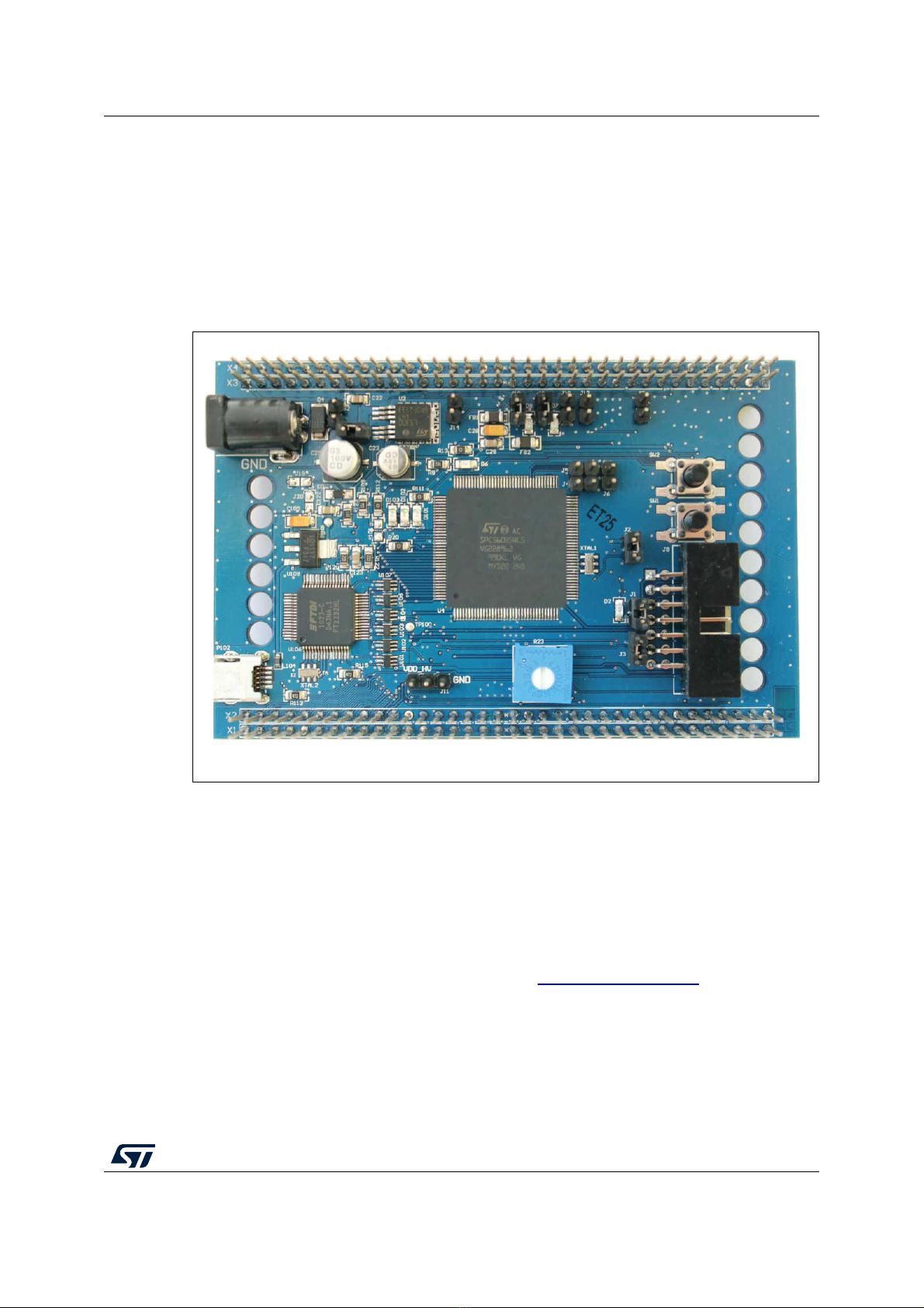
1 SPC56B-DIS discovery board with SPC560B54L5 . . . . . . . . . . . . . . . . . 5
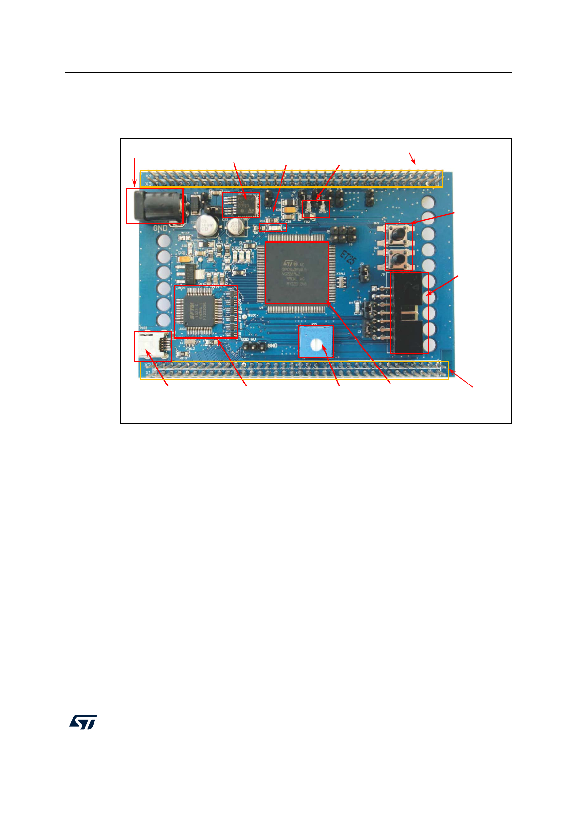
1.1 SPC56B-DIS discovery board . . . . . . . . . . . . . . . . . . . . . . . . . . . . . . . . . . 5
1.2 Debug interface . . . . . . . . . . . . . . . . . . . . . . . . . . . . . . . . . . . . . . . . . . . . . 6
1.3 Microcontroller I/Os . . . . . . . . . . . . . . . . . . . . . . . . . . . . . . . . . . . . . . . . . . 6
2 Hardware overview . . . . . . . . . . . . . . . . . . . . . . . . . . . . . . . . . . . . . . . . . . 7
2.1 Power supply . . . . . . . . . . . . . . . . . . . . . . . . . . . . . . . . . . . . . . . . . . . . . . . 7
2.1.1 12 V DC power supply . . . . . . . . . . . . . . . . . . . . . . . . . . . . . . . . . . . . . . 7
2.1.2 Supply from USB port . . . . . . . . . . . . . . . . . . . . . . . . . . . . . . . . . . . . . . . 8
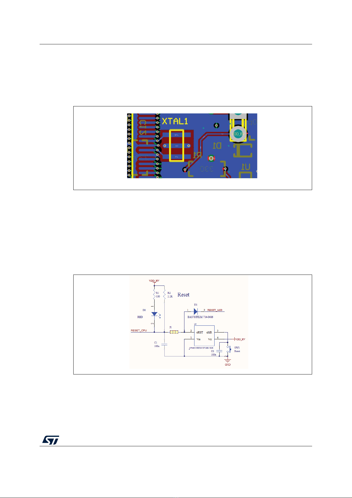
2.2 Crystal oscillator . . . . . . . . . . . . . . . . . . . . . . . . . . . . . . . . . . . . . . . . . . . . . 9
2.3 Reset section . . . . . . . . . . . . . . . . . . . . . . . . . . . . . . . . . . . . . . . . . . . . . . . 9
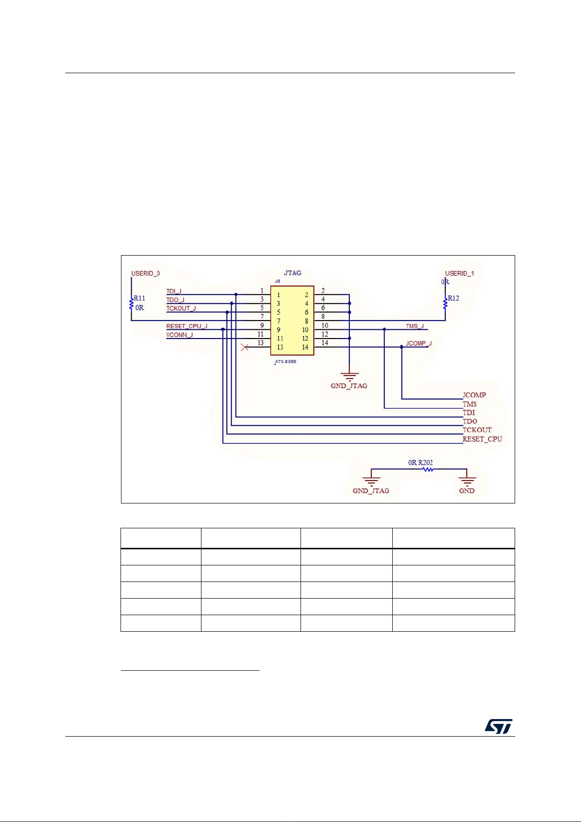
2.4 Programming and debug . . . . . . . . . . . . . . . . . . . . . . . . . . . . . . . . . . . . . 10
2.4.1 JTAG connector . . . . . . . . . . . . . . . . . . . . . . . . . . . . . . . . . . . . . . . . . . . 10
2.4.2 USB with integrated debugger from PLS (default configuration) . . . . . . 11
2.4.3 Board configured as PLS adapter . . . . . . . . . . . . . . . . . . . . . . . . . . . . . 11
2.4.4 HW configuration . . . . . . . . . . . . . . . . . . . . . . . . . . . . . . . . . . . . . . . . . . 11
2.5 USB and Graphic User Interface (GUI) . . . . . . . . . . . . . . . . . . . . . . . . . . 12
2.6 User I/O pins . . . . . . . . . . . . . . . . . . . . . . . . . . . . . . . . . . . . . . . . . . . . . . 13
2.6.1 User LEDs . . . . . . . . . . . . . . . . . . . . . . . . . . . . . . . . . . . . . . . . . . . . . . . 13
2.6.2 Push button . . . . . . . . . . . . . . . . . . . . . . . . . . . . . . . . . . . . . . . . . . . . . . 13
2.6.3 User I/O pins . . . . . . . . . . . . . . . . . . . . . . . . . . . . . . . . . . . . . . . . . . . . . 14
2.6.4 Boot configuration . . . . . . . . . . . . . . . . . . . . . . . . . . . . . . . . . . . . . . . . . 14
2.6.5 ADC input . . . . . . . . . . . . . . . . . . . . . . . . . . . . . . . . . . . . . . . . . . . . . . . 14
2.7 Daughter board connector and I/O headers . . . . . . . . . . . . . . . . . . . . . . . 15
2.8 PCB Layout . . . . . . . . . . . . . . . . . . . . . . . . . . . . . . . . . . . . . . . . . . . . . . . 17
Appendix A General handling precautions . . . . . . . . . . . . . . . . . . . . . . . . . . . . . 19
Appendix B Reference documents . . . . . . . . . . . . . . . . . . . . . . . . . . . . . . . . . . . . 20
Revision history . . . . . . . . . . . . . . . . . . . . . . . . . . . . . . . . . . . . . . . . . . . . . . . . . . . . 21

UM1672 Rev 2 3/22
UM1672 List of tables
3
List of tables
Table 1. +12 V Supply configuration, S1 and S2 jumpers configuration. . . . . . . . . . . . . . . . . . . . . . . 8
Table 2. JTAG connector (pin out) . . . . . . . . . . . . . . . . . . . . . . . . . . . . . . . . . . . . . . . . . . . . . . . . . . 10
Table 3. Programming and debug - Jumper setting . . . . . . . . . . . . . . . . . . . . . . . . . . . . . . . . . . . . . 12
Table 4. I/O headers . . . . . . . . . . . . . . . . . . . . . . . . . . . . . . . . . . . . . . . . . . . . . . . . . . . . . . . . . . . . . 15
Table 5. Document revision history . . . . . . . . . . . . . . . . . . . . . . . . . . . . . . . . . . . . . . . . . . . . . . . . . 21

List of figures UM1672
4/22 UM1672 Rev 2
List of figures
Figure 1. SPC56B-DIS discovery board with SPC560B54L5 . . . . . . . . . . . . . . . . . . . . . . . . . . . . . . . 5
Figure 2. HW overview. . . . . . . . . . . . . . . . . . . . . . . . . . . . . . . . . . . . . . . . . . . . . . . . . . . . . . . . . . . . . 7
Figure 3. +5 V supply section. . . . . . . . . . . . . . . . . . . . . . . . . . . . . . . . . . . . . . . . . . . . . . . . . . . . . . . . 8
Figure 4. Power supply section . . . . . . . . . . . . . . . . . . . . . . . . . . . . . . . . . . . . . . . . . . . . . . . . . . . . . . 8
Figure 5. Crystal (PCB) . . . . . . . . . . . . . . . . . . . . . . . . . . . . . . . . . . . . . . . . . . . . . . . . . . . . . . . . . . . . 9
Figure 6. Reset section . . . . . . . . . . . . . . . . . . . . . . . . . . . . . . . . . . . . . . . . . . . . . . . . . . . . . . . . . . . . 9
Figure 7. JTAG connectors (Schematic and PCB) . . . . . . . . . . . . . . . . . . . . . . . . . . . . . . . . . . . . . . 10
Figure 8. USB connector with integrated debugger from PLS . . . . . . . . . . . . . . . . . . . . . . . . . . . . . . 11
Figure 9. GUI: TX and RX signals with optocoupler . . . . . . . . . . . . . . . . . . . . . . . . . . . . . . . . . . . . . 13
Figure 10. User D7 and D8 LEDs . . . . . . . . . . . . . . . . . . . . . . . . . . . . . . . . . . . . . . . . . . . . . . . . . . . . 13
Figure 11. User push button . . . . . . . . . . . . . . . . . . . . . . . . . . . . . . . . . . . . . . . . . . . . . . . . . . . . . . . . 14
Figure 12. User I/O pins PC4, PA8 and PA9 . . . . . . . . . . . . . . . . . . . . . . . . . . . . . . . . . . . . . . . . . . . . 14
Figure 13. Potentiometers (Schematic & PCB) . . . . . . . . . . . . . . . . . . . . . . . . . . . . . . . . . . . . . . . . . . 15
Figure 14. I/O headers (schematic diagram) . . . . . . . . . . . . . . . . . . . . . . . . . . . . . . . . . . . . . . . . . . . . 16
Figure 15. PCB - Top Layer . . . . . . . . . . . . . . . . . . . . . . . . . . . . . . . . . . . . . . . . . . . . . . . . . . . . . . . . . 17
Figure 16. PCB – Inner Layer 2 . . . . . . . . . . . . . . . . . . . . . . . . . . . . . . . . . . . . . . . . . . . . . . . . . . . . . . 17
Figure 17. PCB – Inner Layer 3 . . . . . . . . . . . . . . . . . . . . . . . . . . . . . . . . . . . . . . . . . . . . . . . . . . . . . . 18
Figure 18. PCB – Bottom Layer . . . . . . . . . . . . . . . . . . . . . . . . . . . . . . . . . . . . . . . . . . . . . . . . . . . . . . 18

UM1672 Rev 2 5/22
UM1672 SPC56B-DIS discovery board with SPC560B54L5
21
1 SPC56B-DIS discovery board with SPC560B54L5
1.1 SPC56B-DIS discovery board
The SPC56B-DIS discovery board is an evaluation tool supporting STMicroelectronics
SPC56 B line microcontrollers. The evaluation board allows full access to all CPUs I/O
signals and to peripherals.
Figure 1. SPC56B-DIS discovery board with SPC560B54L5
The SPC56 B line is STMicroelectronics state of the art MCU based on 32-bit
microcontrollers Power Architecture Cores specifically addressing all Automotive
Applications but as well suitable for industrial safety oriented applications. Such line is
optimized for Body applications as Body Control Modules, Door Modules, Seat controls,
HVAC, Comfort Modules, Security Access and they are suitable for ASIL B/SIL
requirements.
SPC56B-DIS discovery board is supported by a specific application project inside
SPC5Studio (a visual integrated software development environment to easily develop
software for SPC56 MCU's), that embeds micro start-up routines, I/O mapping and a simple
test codes SPC5Studio that is available download www.st.com/spc5studio.
The PCB, the components and all HW parts meet requirements of the applicable RoHS
directives.
GAPGRI00381

SPC56B-DIS discovery board with SPC560B54L5 UM1672
6/22 UM1672 Rev 2
1.2 Debug interface
The microcontroller can be debugged using:
JTAG standard 14 pins interface, for using external debugger tools
USB mini-B, through the PLS debugger integrated on board
1.3 Microcontroller I/Os
All microcontroller IOs are available on the two 2 x 36 headers with exception of JTAG, TCK,
TMS, TDI, TDO, XTAL, EXTAL and VDD_LV pins.

UM1672 Rev 2 7/22
UM1672 Hardware overview
21
2 Hardware overview
Figure 2. HW overview
2.1 Power supply
The discovery board allows wide supply configurations, such as 12 V (external PSU) or 5 V
(USB supply).
2.1.1 12 V DC power supply
12 V voltage can be used to supply the board(a)using the PSU output barrel connector
(+12 V) or directly from 2x36 headers.
The PSU connector shall be center positive with 2.1 mm inner diameters.
The diode D4 protects the boards against the battery reverse connection.
The jumpers S1 and S2 allow choosing the desired 12 V supply. Table 1 depicts the jumper
configuration:
Debugger on board
USB input SPC560B54L5
Reset and
User push
button
User LEDs
Potentiometer
JTAG
connector
+5V LED
2x36pin array
2x36
p
in arra
y
+12V input
Voltage
Regulator
GAPGRI00382
a. If the board is supplied with +12 V, the SMD solder jumpers J19 and J20 can be left opened.

Hardware overview UM1672
8/22 UM1672 Rev 2
The jumper S1 can be used as switch to turn on and off the board.
A linear regulator is used to generate +5 VDC needed for the microcontroller. D4 (green
LED) is connected to voltage regulator output for revealing 5 V presence.
Figure 3. +5 V supply section
2.1.2 Supply from USB port
The board can be fed using the +5 V from the USB cable. To enable this function both
jumpers J19 and J20 have to be closed and the PSU plug can be removed, together with S1
and S2 jumpers.
Figure 4. Power supply section
Table 1. +12 V Supply configuration, S1 and S2 jumpers configuration
S1 S2 +12 V Supply configuration
OPEN OPEN The board is not supplied with 12 V
CLOSE OPEN The board is supplied by the external PSU
CLOSE CLOSE(1)
1. No supply voltage has to be connected to the daughter board.
The discovery board supplies the daughter board (+12 V connected to
the discovery board) or the daughters supplies the discovery (+12 V
connected to the daughter board) (2)
2. Only one of these HW configurations is allowed.
OPEN CLOSE Not used
GAPFRI00383
GAPGRI00384

UM1672 Rev 2 9/22
UM1672 Hardware overview
21
2.2 Crystal oscillator
The SPC56B-DIS board could be populated either with 8 or 16 MHz crystal to clock the
SPC560B54L5.
Default configuration is with 16 MHz crystal.
Figure 5. Crystal (PCB)
2.3 Reset section
In order to generate a clean reset signal for the microcontroller, STM6315RDW13F is used.
SW1 button triggers such device generating a reset signal.
D8 is powered on as soon as reset pulse is generated.
The reset signal can be propagated to the on board linear voltage regulator via
RESET_ASD line closing the jumper J14 (see Figure 3: +5 V supply section).
Figure 6. Reset section
GAPGRI00385
GAPGRI00386

Hardware overview UM1672
10/22 UM1672 Rev 2
2.4 Programming and debug
The microcontroller in the discovery board can be programmed and debugged using two
methods(b):
Staport wndard JTAG connector (male 2x7 100mil - 90°)
USB with integrated debugger.
A further configuration in addition to the previous ones allows to configure the board as a
standalone PLS adapter; in this case, the JTAG connector has to be connected to the target
board adding a passive male-female 2x7 pin adaptor.
2.4.1 JTAG connector
Figure 7. JTAG connectors (Schematic and PCB)
b. A single configuration can be enabled at one time. The jumpers setting to enable the configuration is
described in the paragraph Section 2.4.3: Board configured as PLS adapter.
Table 2. JTAG connector (pin out)
Pin num. Name Pin num. Name
1 TDI 2 GND
3 TDO 4 GND
5 TCK 6 GND
7EVTI 8 NC
9 RESET 10 TMS

UM1672 Rev 2 11/22
UM1672 Hardware overview
21
2.4.2 USB with integrated debugger from PLS (default configuration)
The integrated debugger, based on the device FTDI2232H and UDE PLS software, allows
the user to build, run and debug the software applications. The SPC56B-DIS discovery kit
includes a full-featured, perpetual code-limited (128 Kbytes) PLS software license; the
debugger serial number is reported on a label applied on the bottom side of the board.
To download the debugger software and to activate license go to the PLS website.
The integrated debugger is accessible via ST's free integrated development environment,
SPC5Studio (www.st.com/spc5studio).
Figure 8. USB connector with integrated debugger from PLS
2.4.3 Board configured as PLS adapter
The discovery board can be configured to work as standalone PLS adapter, configuring
jumpers as described below (see Table 3: Programming and debug - Jumper setting). The
board serial number is reported in a label on the board.
A passive adapter can be added to converter from male to female the 2 x 7 JTAG port
soldered on the board. The 3.3 V or 5 V compatibility is achieved by using level shifters
array.
2.4.4 HW configuration
In order to enable one of the previous described functionalities, the board has to be properly
set. The USB integrated debugger is the default configuration.
Table 3 shows how to configure the jumpers also to enable the board as PLS adapter..:
11 VDDE7 12 GND
13 RDY 14 JCOMP
Table 2. JTAG connector (pin out)
Pin num. Name Pin num. Name
GAPGRI00389

Hardware overview UM1672
12/22 UM1672 Rev 2
2.5 USB and Graphic User Interface (GUI)
One of the two FTDI2232 channels has been configured for implementing a serial
communication between PC USB and microcontroller UART, both for serial booting and for
controlling the microcontroller using a dedicated GUI.
The USB section (serial communication) is electrical insulated with respect to all the circuitry
adding opto-couplers in series to the path of TX and SX signals, see Figure 9: GUI: TX and
RX signals with optocoupler .
Table 3. Programming and debug - Jumper setting
Jumper name JTAG USB
(Integrated debugger) PLS Adapter
J101 Open Close Close
J102 Open Close Close
J103 Open Close Close
J105 Open Close Close
J109 Open Close Close
J110 Open Close Close
J111 Open Close Close
J114 Open Close Close
J19 Open Open Close
J20(1)
1. J20 connect the GND of the board to the GND of the USB input. This jumper should be removed when the
USB section must be electrically insulated
Close Close Close
S1(2)
2. S1 is used as power switch; if S1 is left open, the 12V form external source does not supply the board
Close Close Open
S2(3)
3. If S2 is present and the 12V supply comes from the daughters boards, J16 must be left unconnected (no
external PSU must be powered and connected).
Open Open Open
J1 Close Close Close
J2 Close Close Close
J3 Close Close Close

UM1672 Rev 2 13/22
UM1672 Hardware overview
21
Figure 9. GUI: TX and RX signals with optocoupler
2.6 User I/O pins
Some microcontroller GPIOs are dedicated for user purpose. Here below details about each
group.
2.6.1 User LEDs
The LEDs D7 and D8 are available for user purpose; the jumpers J9, J10 connect the 2
LEDs to the microcontroller I/O PC3 and PC2 respectively. The HW connection is reported
in Figure 10: User D7 and D8 LEDs.
Figure 10. User D7 and D8 LEDs
2.6.2 Push button
A push button is connected to GPIO PA11. The pin is connected to High level by a 10 kΩ
pull-up resistor and it is set to Low (GND) when the button is pushed; a low pass filter has
been added to reduce the noise and clean spurious signals.
GAPGRI00390
GAPGRI00391

Hardware overview UM1672
14/22 UM1672 Rev 2
Figure 11. User push button
2.6.3 User I/O pins
Pin PC4 can be set to Low or High configuring J11.
Figure 12. User I/O pins PC4, PA8 and PA9
2.6.4 Boot configuration
It is possible to reprogram microcontroller internal Flash programming to use Boot Assist
Mode (BAM) via SCI. The pins PA8 and PA9, (see Figure 12: User I/O pins PC4, PA8 and
PA9) have to be configured to enable the BAM functionality as following:
FABM (PA9) has to be connected to VDD_HV to enable serial boot (J13 jumper
closed).
ABS (PA8) has to be physically grounded to flash via SCI (J12 jumper closed).
If the BAM function is not used, these pins can be configured as normal I/O according to the
functions reported in the datasheet (see Section Appendix B: Reference documents).
2.6.5 ADC input
A trimmer connected to the microcontroller PB8 input allows the user to check ADC. The
analog input voltage range is 0V ÷ VDD_HV.
GAPGRI00392
GAPGRI00393

UM1672 Rev 2 15/22
UM1672 Hardware overview
21
Figure 13. Potentiometers (Schematic & PCB)
2.7 Daughter board connector and I/O headers
The I/O microcontroller pins are connected to a double 2 x 36 pin array (connectors X1-X2
and X3-X4).
GAPGRI00394
Table 4. I/O headers
Pin number X1 X2 X3 X4
1 GND GND VBAT VBAT
2 PE[2] PE[3] GND GND
3PC[5]PC[4]TCKTDI
4 PE[4] PE[5] TDO TMS
5 PH[4] PH[5] PA[6] PA[5]
6 PH[6] PH[7] PC[2] PC[3]
7 PH[8] PE[6] PG[11] PG[10]
8 PE[7] PC[12] PE[15] PE[14]
9 PC[13] PB[1] PG[15] PG[14]
10 PB[2] PB[3] PE[12] PA[11]
11 GND GND GND GND
12 PB[0] PC[14] PA[10] PA[9]
13 PC[15] PG[5] PA[8] PA[7]
14 PG[4] PG[3] PE[13] PF[14]
15 PG[2] PA[2] PF[15] PG[0]
16 PE[0] PA[1] PG[1] PH[3]
17 PE[1] PE[8] PH[2] PH[1]
18 PE[9] PE[10] PH[0] PG[12]
19 PA[0] PE[11] PG[13] PA[3]
20 Reset ASD PG[9] PB[15] PD[15]
21 PG[8] PC[11] PB[14] PD[14]

Hardware overview UM1672
16/22 UM1672 Rev 2
Figure 14. I/O headers (schematic diagram)
22 GND GND GND GND
23 PC[10] PG[7] PB[13] PD[13]
24 PG[6] PC[9] PB[12] PD[12]
25 PC[8] PF[9] PB[11] PD[11]
26 PF[8] PF[12] PD[10] PD[9]
27 PC[6] PC[7] PB[7] PB[6]
28 PF[10] PF[11] PB[5] PB[4]
29 PA[15] PF[13] PD[8] PD[7]
30 PA[14] PA[4] PD[6] PD[5]
31 PA[12] PA[13] PD[4] PD[3]
32 PB[9] PB[8] PD[2] PD[1]
33 PB[10] PF[0] PD[0] PF[7]
34 PF[1] PF[2] PF[6] PF[5]
35 GND GND PF[4] PF[3]
36 5V 5V GND GND
Table 4. I/O headers (continued)
Pin number X1 X2 X3 X4

UM1672 Rev 2 17/22
UM1672 Hardware overview
21
2.8 PCB Layout
Figure 15. PCB - Top Layer
Figure 16. PCB – Inner Layer 2
GAPGRI00399
GAPGRI00400

Hardware overview UM1672
18/22 UM1672 Rev 2
Figure 17. PCB – Inner Layer 3
Figure 18. PCB – Bottom Layer
GAPGRI00401
GAPGRI00402

UM1672 Rev 2 19/22
UM1672 General handling precautions
21
Appendix A General handling precautions
The following precautions are recommended when using the SPC56B-DIS, discovery
board:
Do not modify or manipulate the board when the external PSU supply is powered and
connected to the board.
Do not open and modify the PSU. Use AC plug adaptor if the main socket is not
compatible with the PSU plug.
Do not supply the board with a DC source higher than 12 V.
Any equipment or tool used for any manipulation of the semiconductor devices or
board modification should be shielded and connected to ground.
The connectors and cables should be plugged and removed when the board is not
supplied.
It is recommended to use antistatic tools.

Reference documents UM1672
20/22 UM1672 Rev 2
Appendix B Reference documents
32-bit MCU family built on the Power Architecture®for automotive body electronics
applications (Datasheet, Doc ID 15131).
Table of contents
Other ST Motherboard manuals

ST
ST STM8/128-EVAL User manual

ST
ST STEVAL-IHM022V1 User manual

ST
ST UM1789 User manual

ST
ST VIPower VIPer22A-E Installation and operating instructions

ST
ST EVAL-L99MOD5xXP User manual

ST
ST STM3220F-EVAL User manual

ST
ST STEVAL-ILH007V1 User manual

ST
ST STM3221G-EVAL User manual

ST
ST UM0920 User manual

ST
ST STEVAL-ISB68RX User manual

ST
ST SPC58XXADPT144S REV.B User manual

ST
ST STM8L1526-EVAL User manual

ST
ST NUCLEO-G070RB User manual

ST
ST STM32L4R9I-EVAL User manual

ST
ST STM3240G-EVAL User manual

ST
ST STM3210E-EVAL User manual

ST
ST STM3241G-EVAL User manual

ST
ST STEVAL-PCC010V1 User manual

ST
ST STM32429I-EVAL User manual

ST
ST STR730-EVAL User manual