ST STEVAL-LLL014V1 User manual

Introduction
The STEVAL-LLL014V1 is a four LEDs strings evaluation kit based on the ALED7709 LED driver
This kit consists of :
• a control board (STEVAL-LLL014M1), based on the ALED7709 LED driver and SPC582B60E1 microcontroller
• a LED board (STEVAL-LLL014D1) hosting the KW DPLS33.KD OSRAM LEDs and Murata NTC
Figure 1. STEVAL-LLL014V1
Getting started with the STEVAL-LLL014V1 kit based on ALED7709 LED driver
UM3180
User manual
UM3180 - Rev 1 - May 2023
For further information contact your local STMicroelectronics sales office. www.st.com

1Overview
The STEVAL-LLL014V1 consists of:
• a four LED strings board (STEVAL-LLL014D1)
• a control board (STEVAL-LLL014M1) based on the ALED7709 LED driver.
The ALED7709 is an automotive LED driver (AEC-Q100 Grade1 qualified), it is connected in boost topology and
controlled by the MCU SPC582B60E1.
The ALED7709 includes a DC/DC controller usable as boost or SEPIC, and four low-side constant-current
sinkers. The benefit of having the DC/DC controller integrated with the LED sinkers is the possibility of adapting
the output voltage for the different LED conditions. This minimizes the power dissipation of the LED driver and
therefore increases overall efficiency. The SPC582B60E1 is a 32bit automotive grade microcontroller used to
control the ALED7709 via the I²C interface.
The STEVAL-LLL014V1 can be configured and controlled with the STSW-LLL014GUI SW.
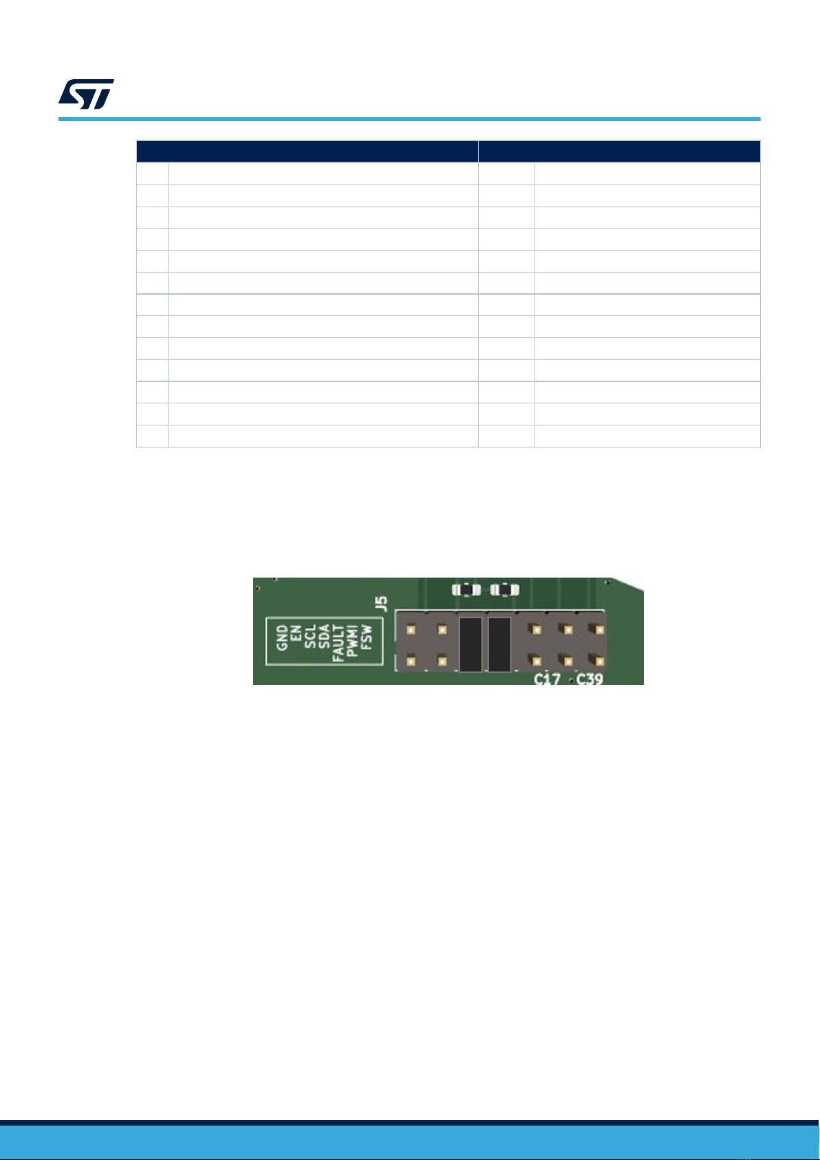
The kit is designed in the way that ALED7709 can be disconnected from the on board MCU opening all J5
jumpers. J5 can be used as the input connector for any other I²C system.
ALED7709 is suitable to support automotive lighting and backlight applications; like cluster/infotainment display,
head-up display (HUD), instrument lighting system, or ambient light.
The ALED7709 can operate from a DC supply voltage between 4.5V to 42V. The input divider on the EN pin has
been set to block the converter functionality below 6V showing the double threshold capability.
The STEVAL has been optimized for a switching frequency of 400KHz set through an external resistor. The
switching frequency can be adjusted/synchronized using the FSW signal generated by MCU or supplied from an
external source.
Switching frequency can be also derived from the internal oscillator properly setting the BOOSTCFG register.
The spread spectrum can be enabled or disabled for both configurations to reduce the electromagnetic emission.
Another way to keep under control the emission is to enable the phase-shift for the PWM dimming. To avoid a
large current peak absorbed, phase shift can delay each channel by a quarter of the PWM period.
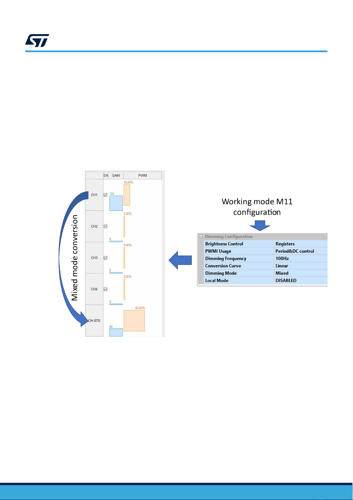
Dimming can be controlled in different ways:
• by I²C registers, by PWMI signal, or using both at the same time
• using digital dimming and/or analog dimming as independent control, or using the mixed PWM and analog
defined by ALED7709
Using the appropriate register setting, it is possible to dim all the channels at the same level (global dimming) or
each one independently (local dimming).
STEVAL-LLL014D1 includes jumpers to create OPEN and/or SHORT faults to check the autodisconnect feature.
This can be enabled or disabled in the FMCFG register.
The maximum current per channel has been set to 150mA to give enough margin to the LED used in STEVAL-
LLL014D1. The current can be reduced acting on the GAIN registers. While to increase the value up to 200mA,
the maximum supported by ALED7709, it is necessary to change the R12.
STEVAL-LLL014D1 has an NTC to allow ALED7709 keeping under control the LED temperature. This feature can
be enabled or disabled in the OUTCFG register.
Figure 2. STEVAL-LLL014V1 Block diagram
UM3180
Overview
UM3180 - Rev 1 page 2/29

2Get started with the board
Join the STEVAL-LLL014D1 to the STEVAL-LLL014M1 (with STSW-LLL014FW on board) through the connector
J3.
Connect a mini-USB cable between the PC and the connector J1.
Apply the power supply VIN to the connector J2; a power supply capable of at least 6A is required.
Figure 3. STEVA-LLL014M1 connectors
Table 1. Connectors description
Mini USB (J1) STEVAL-LLL014D1 connector (J3)
1VBUS 1 CH1: Cathode LED string
2 D- 2 CH1: Anode LED string
3 D+ 3 CH2: Cathode LED string
4 GND 4 CH2: Anode LED string
5 CH3: Cathode LED string
Power supply (J2) 6 CH3: Anode LED string
1Positive terminal of power supply: VIN 7 CH4: Cathode LED string
2 Negative terminal of power supply: GND 8 CH4: Anode LED string
9 NTC connection
Interface connector (J5) 10 GND
1 GND
2 GND JTAG connector (J4)
3 Enable signal from MCU 1 TDI
UM3180
Get started with the board
UM3180 - Rev 1 page 3/29

Mini USB (J1) STEVAL-LLL014D1 connector (J3)
4 Enable signal to ALED7709 2 GND
5 SCL from MCU 3 TDO
6 SCL to ALED7709 4 GND
7 SDA from MCU 5 TCK
8 SDA to ALED7709 6 GND
9 FAULT signal to MCU 7 N.C.
10 FAULT signal from ALED7709 8 N.C.
11 PWMI signal from MCU 9 NRST
12 PWMI signal to ALED7709 10 TMS
13 FSW signal from MCU 11 3V3
14 FSW signal to ALED7709 12 GND
13 N.C.
14 JTNRST
The connector J4 is dedicated to SPC582B60E1, it allows users to update the firmware if needed, or to develop
a specific code. The three buttons on the STEVAL-LLL014M1 have been added as usable resources for firmware
developers.
Be sure to have closed at least the two I²C jumpers on the connector J5, as shown in the figure below.
Figure 4. SCL and SDA jumpers on J5 connector
STSW-LLL014GUI communicates to the STEVAL boards using a USB port. FTDI drivers (www.ftdi.com) need to
be installed on a Windows 10 PC/laptop.
Connect the mini-USB cable from a PC to the STEVAL-LLL014M1 board then run the GUI launching the file
STSW-LLL014GUI.exe.
If the board is not yet connected to the PC, on the upper bar appears the indication “No Bridge connected” and
only the “00” device icon is present.
When the connection is established, a new “28” device icon appears. The bridge status changes to “Bridge
connected (firmware x.y)”; where x.y is the revision number of firmware loaded inside the MCU. It acts as bridge/
interpreter for the communication to ALED7709.
On the upper bar, there is also the indication of the STSW-LLL014GUI version.
The graphical user interface appears as per the figure below:
UM3180
Get started with the board
UM3180 - Rev 1 page 4/29

3GUI usage
The main window can be divided into different sections that are detailed in the following paragraphs.
Figure 7. Main window sections
3.1 Top bar
Top bar reports the STSW-LLL014GUI version, the board connection status, and the firmware revision.
Figure 8. Top bar
3.2 File management
This section includes two buttons: Load and Save.
Save allows storing the configuration of the device in a file. It opens a dialog box to input the file name and to
choose the folder where to save it; the default file extension used is .cfg.
Load opens a dialog box as well to locate the wanted configuration file, clicking on the Open button the file
content is applied to the device.
UM3180
GUI usage
UM3180 - Rev 1 page 6/29

Figure 9. File configuration manager and example of configuration file
3.3 Device toolbar
The indication “Bridge connected” into the top bar confirms that a STEVAL-LLL014M1 board is properly
connected and recognized.
Once the communication is established, the GUI checks the ALED7709 presence. As soon as the device replies
to the inquiry:
• the message “Devices Found: 1” is displayed on the bottom left corner of the GUI window
• the device button “28” is shown on the device toolbar.
Figure 10. Device toolbar buttons and device presence message
VIRTUAL device button “00” is always present and selectable, even without a board connected. This selection,
as the name suggests, is a simulated device on virtual memory and does not use any external communication. It
allows playing with the GUI and creating a configuration that can be saved in a file. This file can be loaded into
any device, once available.
Pressing the button “28” the I²C address is acquired by the GUI. The content of the ALED7709 registers is
loaded into the GUI memory and the Main window is updated as consequence. Optionally, the uploading process
can be forced anytime by pressing the Reload button.
Enable button sets and resets the DEN bit in the DEVEN register. This brings the ALED7709 in operational mode
from standby and vice versa.
3.4 Device status
The “Device status” section shows the content of the status registers: DEVSTA, CHSTA, and INITSTA. Whose
content can be reset by clicking on the CLEAR button. In case the reported FAULT is still present, the information
is immediately set again.
Figure 11. Device status indication and Clear button
UM3180
Device toolbar
UM3180 - Rev 1 page 7/29

For detailed explanation of each bit, please refer to the ALED7709 datasheet.
3.5 Device settings
In the “Device settings” section, there is the possibility to configure the way of working of ALED7709.
It contains the following subsections:
• fault management
• fault pin management
• output configuration
• boost configuration
• dimming configuration
Figure 12. Fault management subsection
The fault management subsection acts on the bits inside the FMCFG register.
It is possible to enable or disable the protections associated to the PMOS presence. In STEVAL-LLL014M1, the
PMOS is present, so the “External PMOS” must be set YES, otherwise, the power supply does not reach the
boost section. To test the functionality setting “External PMOS” as NO, it is necessary to short circuit Source and
Drain of Q1.
Figure 13. Fault pin management subsection
Fault pin management acts on the FMASK register, it is possible defining which fault is externally signalized using
the FAULT pin. On STEVAL-LLL014M1, the FAULT pin drives the D4 LED to indicate when a not masked fault is
detected. For firmware developers, it is possible connecting the FAULT pin to the MCU, closing the FAULT jumper
on the J5. This signal can be used as a FAULT interrupt for any specific action.
Figure 14. FAULT jumper closed on J5
UM3180
Device settings
UM3180 - Rev 1 page 8/29

Figure 15. Output configuration subsection
Output configuration subsection controls the bits inside the OUTCFG register.
“Temp Sensing” can be DISABLED simply acting on the bit; the NTC can be left connected.
Figure 16. Boost configuration subsection
Boost configuration subsection adjusts the bits inside the BOOSTCFG register.
In this subsection, it is possible to adjust the boost switching frequency; selecting External, R6 sets the switching
frequency to about 400KHz. Otherwise, it is possible to select a fixed switching frequency of 400KHz, 800KHz or
1.6MHz derived as division of the internal Main Clock of 6.55MHz.
It is suggested to put the system in standby (acting on the Enable button) before selecting a different switching
frequency. The choice of R6 at 61.8KΩ is to allow a seamless transition between External and 400KHz internal.
Main Clock Spread Spectrum can be enabled or disabled in any condition because Main Clock is always running.
Even if the “Spread Spectrum External Freq.” is ENABLED, it is active only if the switching frequency is set as
External.
Figure 17. Dimming configuration subsection
Dimming configuration subsection is used to select one of the 14 working modes reported in the datasheet, it acts
on the DIMCFG register.
Please refer to the datasheet for a detailed explanation of each working mode.
Here to set the way to control the brightness (by register, PWMI or both) and the curve applied to the brightness
(Linear or Exponential). To define the dimming frequency (if applicable) and the PWM and GAIN management
(User or Mixed). To select if the four channels must be driven together (Global mode) or independently (Local
mode).
3.6 Channels settings
Each channel of the ALED7709 can be configured acting in the “Channel settings” section. Channels can be
adjusted separately or globally; it depends on the Local mode setting in the dimming configuration subsection.
UM3180
Channels settings
UM3180 - Rev 1 page 9/29

If Global mode is selected, PWM and GAIN of CH1 are applied to all the active channels. While in Local mode,
each channel uses the setting of its PWM and GAIN.
Each bar can be modified dragging it by the mouse, selecting it by double-click and writing the needed value with
the keyboard.
Channel enable (EN flags) is always active for the specific channel in any working mode.
PWM information is always in percentage, but it has a different reference for the Linear or the Exponential
conversion curve. For the Linear curve, the percentage is related to the maximum value defined by dimming
frequency (please refer to paragraph 7.9.1 of the datasheet). While for the Exponential curve, the percentage is
always related to 8bit value.
When dimming mode is set as Mixed, the GAIN bar/value is no longer used and the PWM bar/value becomes
the only used brightness parameter. When Mixed mode is active, the device computes internally the analog and
digital dimming to be used. The CH-STS bars, placed just below CH4 in the Channel settings area, show the
resulting values.
Figure 18. STS registers information when in Mixed mode
3.7 Hardware Controls window
In the Main toolbar area, there is the HW Controls button, click on it to open the Hardware Controls window.
From this window, it is possible to adjust the PWMI and FSW signals, they are generated inside the MCU and
used to control the ALED7709.
UM3180
Hardware Controls window
UM3180 - Rev 1 page 10/29

Figure 19. Hardware Controls window
Each bar can be modified dragging it by the mouse, selecting it by double-click and writing the needed value with
the keyboard.
The relative jumpers in J5 must be closed to connect the signals from MCU to the correspondent ALED7709 pins.
Figure 20. PWMI and FSW jumpers on J5
EN pin can be connected to the MCU closing the appropriate jumper on J5 (blue jumper in next figure). Or it can
be manually controlled, to force the ALED7709 in shut-down, shorting the EN pin to GND (red jumper in the next
figure).
Figure 21. EN pin connection: to MCU or manually to GND
3.8 Register configuration window
Click on the Registers button, present in the Main toolbar area, to open the Register configuration window.
This window shows in a single grid all the bits of each register of ALED7709.
UM3180
Register configuration window
UM3180 - Rev 1 page 11/29

Figure 22. Register configuration window
The REGISTER column identifies the register using the same datasheet name. The ADDR column is the register
address, and the DATA column is its content. Both values are in hexadecimal format.
The numbered columns give the name of each bit of every register; for a detailed description of each bit
functionality please refer to the datasheet.
All the registers are 8bit, but PWMx, for easy reading, are represented in 16bit concatenating PWMH and PWML.
The content of each Write register can be changed acting on the DATA column or modifying the single bit field.
Read only registers cannot be edited.
Any content change done in the Register configuration window is reflected in the Main GUI window and vice
versa. In both cases, all the changes are applied to the device.
3.9 Log window
The STSW-LLL014GUI monitors continuously the I²C communication with the ALED7709.
Pressing the Log button, in the Main toolbar area, display the Log window.
Figure 23. Log window
UM3180
Log window
UM3180 - Rev 1 page 12/29

Each Log line reports the following info:
TIME : is the time, relative to the GUI start, of when the I²C packet has been transmitted;
newer packets are placed on top for an easier check.
DEV : is the I²C device address in 7bit hex.
BUS : is the direction of the communication: R–read from device; W–write to device.
ADDR : is the lowest address, in hex, of the registers to be used.
DATA : reports all the data transferred in the packet; the leftmost is related to the lower address.
The log acquisition is started/stopped by pressing the Green arrow icon. Click the Brush icon to clean the Log
lines.
It is possible to exclude from the Log lines the record of communication packets addressed to specific registers.
This is achieved adding the ADDR value in the Log mask field; in this way, the I²C operations involving those
registers are executed but not displayed.
UM3180
Log window
UM3180 - Rev 1 page 13/29

4PCB
Figure 24. STEVAL-LLL014M1 top silkscreen
Figure 25. STEVAL-LLL014M1 bottom silkscreen
UM3180
PCB
UM3180 - Rev 1 page 14/29

Figure 26. STEVAL-LLL014M1 top Layer
Figure 27. STEVAL-LLL014D1 top silkscreen
UM3180
PCB
UM3180 - Rev 1 page 15/29

Figure 28. STEVAL-LLL014D1 bottom silkscreen
Figure 29. STEVAL-LLL014D1 top Layer
UM3180
PCB
UM3180 - Rev 1 page 16/29

Figure 30. STEVAL-LLL014D1 bottom Layer
UM3180
PCB
UM3180 - Rev 1 page 17/29

5Schematic diagrams
Figure 31. STEVAL-LLL014M1 schematic diagram
ALED7709ATR
UM3180 - Rev 1 page 18/29
UM3180
Schematic diagrams

Figure 32. STEVAL-LLL014D1 schematic diagram
UM3180 - Rev 1 page 19/29
UM3180
Schematic diagrams

6BOM
Table 2. STEVAL-LLL014V1 bill of materials
Item Q.ty Ref. Part / Value Description Manufacturer Order code
1 1 - Table 3. STEVA
L-LLL014M1 Control board ST Not available for separate
sale
2 1 - Table 4. STEVA
L-LLL014D1 LED board ST Not available for separate
sale
Table 3. STEVAL-LLL014M1 bill of materials
Item Q.ty Ref. Part / Value Description Manufacturer Order code
1 17
C1, C3, C8,
C10, C11, C12,
C13, C16, C17,
C18, C34, C35,
C36, C37, C39,
C41, C42
100n 16V Ceramic Capacitor Murata GCJ188R71C104KA01#
2 2 C2, C38 10n 25V Ceramic Capacitor Murata GCJ188R71E103KA01#
3 1 C4 10u 10V Ceramic Capacitor Murata GRT188D71A106ME73#
4 4 C5, C25, C29,
C50 1u 16V Ceramic Capacitor Murata GCM188R71C105KA64#
5 2 C6, C7 47p Ceramic Capacitor Murata GCM1885C2A470GA16#
6 1 C9 4.7u 16V Ceramic Capacitor Murata GRT188C71C475KE13#
7 2 C14, C15 18p Ceramic Capacitor Murata GCM1885C2A180GA16#
8 5 C19, C21, C43,
C44, C45 4.7u 100V Ceramic Capacitor Murata GCJ32DC72A475KE01#
9 1 C20 22n 25V Ceramic Capacitor Murata GCJ188R71E223KA01#
10 1 C22 100p Ceramic Capacitor Murata GCM1885C2A101GA16#
11 1 C24 1u 16V Ceramic Capacitor Murata GCJ21BR71C105KA01#
12 4 C26, C27, C28,
C31 10u 50V Ceramic Capacitor Murata GCM31CD71H106KE36#
13 1 C30 1u 100V Ceramic Capacitor Murata GCJ21BC72A105KE02#
14 1 C32 EEHZC1K470P Polarized
Capacitor Panasonic EEHZC1K470P
15 1 C33 1u 50V Ceramic Capacitor Murata GCJ21BR71H105KA01#
16 1 C40 470n 16V Ceramic Capacitor Murata GCJ188R71C474KA12#
17 1 C46 63SXV100M Polarized
Capacitor Panasonic 63SXV100M
18 3 C47, C48, C49 100n 100V Ceramic Capacitor Murata GCJ188R72A104KA01#
19 1 D1 STPS1H100AY,
SMA Power Diode ST STPS1H100AY
20 1 D2 STPS2L60AY,
SMA Power Diode ST STPS2L60AY
21 1 D3 KP-2012LSGC LED SMD GREEN Kingbright KP-2012LSGC
22 1 D4 KPT-2012SURC
KLED SMD RED Kingbright KPT-2012SURCK
23 1 J1 USB_B_Mini USB Mini
Connector Wuerth 65100516121
UM3180
BOM
UM3180 - Rev 1 page 20/29
Table of contents
Other ST Motherboard manuals

ST
ST ST72F651 User manual

ST
ST L5965 User manual

ST
ST STEVAL-L99615C User manual

ST
ST STLINK-V3SET User manual

ST
ST STEVAL-IHM022V1 User manual

ST
ST STM32L1 Series Installation and operating instructions

ST
ST STUSB03E User manual

ST
ST STA333ML Installation and operating instructions

ST
ST STEVAL-IHM022V1 User manual

ST
ST STEVAL-AKI001V1 User manual

ST
ST STEVAL-L6982CDR User manual

ST
ST STEVAL-ILH007V1 User manual

ST
ST EVAL-FDA903U-SA User manual

ST
ST AEKD-USBTYPEC1 User manual

ST
ST STM32303E-EVAL User manual

ST
ST STEVAL-LVLP01 User manual

ST
ST STEVAL-ILL059V1 User manual

ST
ST X-NUCLEO-IKS01A1 User manual

ST
ST STSW-IDS002V1 User manual

ST
ST EVAL-7803APSO-SA User manual