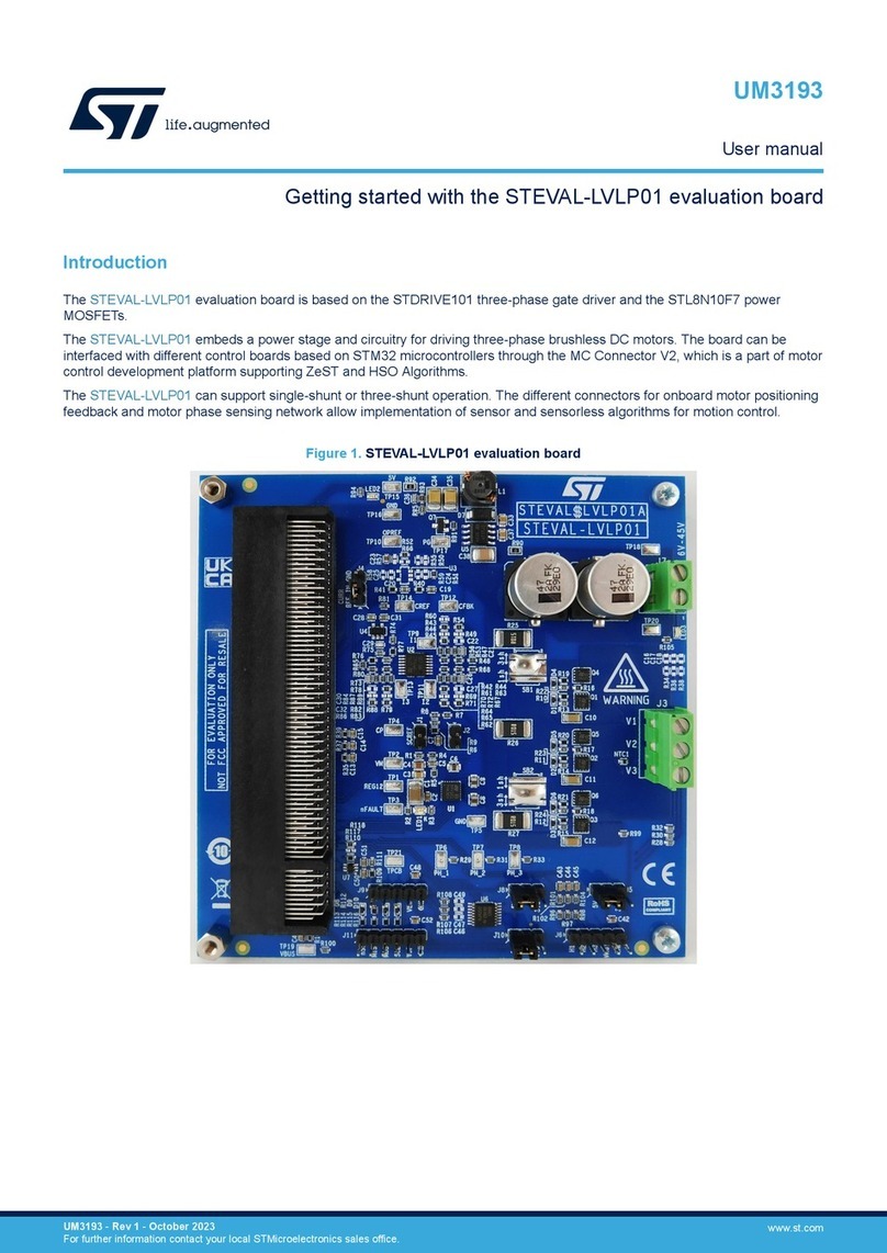
ST STEVAL-AKI001V1 User manual

Introduction
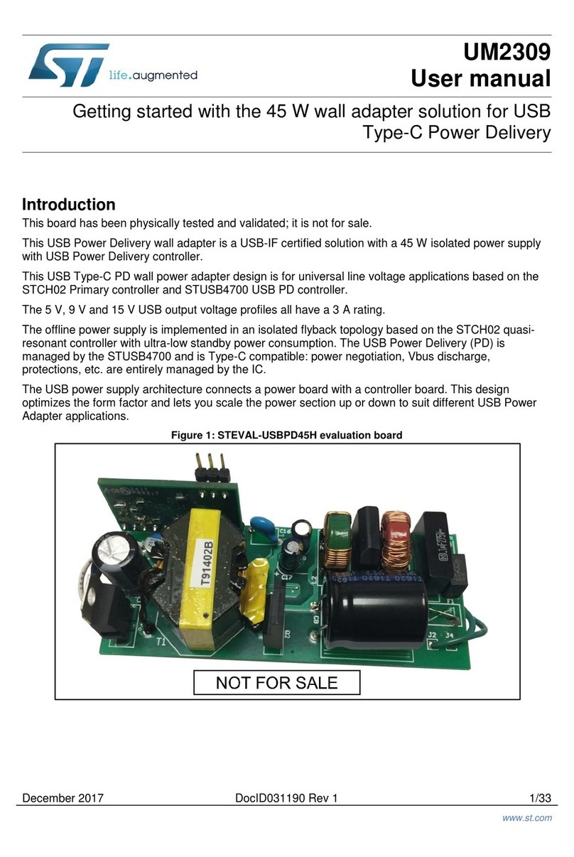
The STEVAL-AKI001V1 evaluation board allows the user to evaluate the conversion performance of the ADC120 8-channel
analog-to-digital converter designed for 50 ksps to 1 Msps conversion.
The board has several on-board sources like temperature sensor and strain gauge signals, and can accept external signals to
allow measurement and evaluation of the ADC120 conversion performance based on its successive approximation register
(SAR) with internal track-and-hold cell.
The board is supplied ready-to-use in standalone mode, or it can be plugged onto a NUCLEO-L476RG board with SMT32
microcontroller, which enables further signal processing and PC communication.
Figure 1. STEVAL-AKI001V1 evaluation board for the ADC120
How to use the evaluation board for the ADC120 8-channel analog to digital
converter
UM2691
User manual
UM2691 - Rev 2 - September 2020
For further information contact your local STMicroelectronics sales office.
www.st.com

1Board overview
The board inputs are configured on the following J2 connector pins:
•Pin 8 (In3): input for ±5V signal
• PIN 10 (In4): input configurable to measure around 1.7 V reference voltage or external 0 to 3V3 voltage
(selected using jumper J31)
• Pin 12 (In5): input for 0 to 3V3 signal (no filtering)
• Pin 14 (In6): input not directly connected, footprints are left to the user to allow amplification
• Pin 16 (In7): input not directly connected, footprints are left to the user to allow amplification
Figure 2. STEVAL-AKI001V1 block diagram
The STEVAL-AKI001V1 evaluation board includes the following hardware functionality:
•2.54mm, 38cts double female connectors to be plugged to the STM32L476RG Nucleo development board
(J1)
• 2.54mm, 10cts, double male connector to connect an SPI to UART communication module (J3)
• Several configuration jumpers to select power supply input
• 3V3 LDO for power supply (JP4 5V jumper and JP5 LDO 3V3)
• A TS3431 voltage reference
• An analog to digital converter ADC120 SAR, 12 bits, 8 inputs (IN0 to IN7)
• An STLM20 temperature sensor on IN0
• A PT100 resistance thermometer on IN1
• Acquisition of a ±5V signal on IN3
• Voltage reference sampling necessary for precise calculations
• Sampling of a 0 to 3V3 voltage input
• Acquisition of amplified inputs (not connected) configurable by the user on 2 channels (IN6 and IN7)
• Instrumentation amplifier for a strain gauge on IN2
The SPI communication lines are connected to the SPI communication lines of the STM32L476RG Nucleo
development board and to the connector dedicated to the SPI to UART communication module. The jumpers are
configured in the following way:
• JP4 - 5VNUC
• JP5 - AVCC
UM2691
Board overview
UM2691 - Rev 2 page 2/27
• J31 - VREF
•J44 - GND
UM2691
Board overview
UM2691 - Rev 2 page 3/27

2Board connection and operation
2.1 Power supply
The power supply input can be selected form the following sources:
•5V from Nucleo board or external supply (if Nucleo is not used)
• 3V3 voltage from Nucleo development board.
JP4 enables the 3V3 LDO that converts the 5V into 3V3.
JP5 chooses between 3V3 vai the LDO and 3V3 from the Nucleo
Figure 3. Power supply selection jumpers
C16
1µF
GND
GND
C14
1µF
C17
1µF
C18
0.1µF
GND
3.3V_NUCLEO
DVCC
3.3V_D Generate
JP4
DVCC Generate
JP5
GND
GND
IN
1
EN
3
GND
2
4
5
IC11
LDK220M
5V_NUCLEO
AVCC
ADJ/NC
OUT
2.2 SPI communication
The ADC120 has the following SPI communication inputs and oututs
•DIN line is MOSI (Master Output Slave Input)
• DOUT line is MISO (Master Input Slave Output)
• SCLK line is the clock
• CS line is Chip Select
UM2691
Board connection and operation
UM2691 - Rev 2 page 4/27

Figure 4. ADC120 SPI timing diagram
2.3 Board operation
The ADC120 channel to be read can be selected by sending the proper code through the DIN (MOSI) line.
The reading on DOUT provides the converted raw data. A code running inside a microcontroller can calculate the
proper value in volts or in degrees Celsius, depending on the analog sensor used.
RELATED LINKS
Visit the ST website to download application note AN5454
UM2691
Board operation
UM2691 - Rev 2 page 5/27

3STEVAL-AKI001V1 ADC inputs
3.1 ADC channel 0: temperature measurement
The input channel 0 on the ADC120 receives the converted output from the STLM20 analog temperature sensor
on the evaluation board.
Figure 5. STEVAL-AKI001V1 schematic - temperature measurement with STLM20
NC
1
GND
2
VOUT 3
VCC 4
GND
5
IC51
STLM20
R60
470
AVCC
ADC_0
SBR0220T5-7
D51
NC
C55
0.1µF
GND
GND
C53 0.1µF
GND
AVCC
AVCC
The voltage V (V) image of the temperature T (°C) is given by the following equation:
VADC0=−3.88*106*T2+−1.15*10−2*T+ 1.8639 (1)
RELATED LINKS
Visit the STLM20 product page on the ST website for more information regarding this device
3.2 ADC channel 1: temperature measurement
The input channel 1 on the ADC120 receives the voltage image of the PT100 resistor on the evaluation board.
Figure 6. STEVAL-AKI001V1 schematic - temperature measurement with PT100
Rref
698
PT100
100 C57
10nF
ADC_1
R64
330
C59
10nF
SBR0220T5-7
D52
NC
AVCC
GND
GND
AVCC
C54 22nF
GND
V_REF
R55
3.6K
R56
3.6K
R57
1.8K
GND
R58
1.8K
GND
R59
1.8K
V+
V-
+
3-
2
1
4 8
IC52A
TSU112
+5
-6
7
IC52B
TSU112
GND
4
5
+
1
-
3
2
V+
V- IC53
TSU111
R62
2K
R63
20K
GND
AVCC
C58 10nF
GND
GND
C52
10µF
C51
0.1µF
The resistance R100 image of the temperature is given by the following equation:
UM2691
STEVAL-AKI001V1 ADC inputs
UM2691 - Rev 2 page 6/27

RPT100 =VADC1*2*Rref
11*Vref (2)
And the temperature T is given by:
T=
RPT100
R0−1
α(3)
Where:
•R0=100Ω is the resistance at 0 °C
•α=0.00385
Ω
Ω
°C is the temperature coefficient
3.3 ADC channel 2: input for strain gauge measurement
The ADC120 input channel 2 measures and amplifies the strain gauge variation via a Wheatstone bridge.
Figure 7. STEVAL-AKI001V1 schematic - instrumentation amplifier for strain gauge measurement
R43
120
R44
120
R45
120
R46
EXTERNAL RESITOR
AVCC
ADC_2
0.1%
R48
1K
Strain gauge - R=120 ohms
GND
GND
FSG +
J41
FSG -
J42
Strain_gauge_ref
Strain Gauge Set
J44
AVCC
V-_Wheatstone
V+_Wheatstone
C4122nF
GND
0.1%
R47
20K
0.1%
R49
20K
0.1%
R50
33K
0.1%
R51
33K
C4322nF
GND
AVCC
GND
0.1%
R52
33K
0.1%
R53
33K
1
5
+
3
-
4
2
V+
V- IC42
TSZ121
R54
330
C44
10nF
SBR0220T5-7
D41
NC
AVCC
GND
V+
V-
+
3
-
2
1
4 8
IC41A
TSZ122
+
5-
6
7
IC41B
TSZ122
J43
GND
AVCC
The ADC120 reads the voltage image of the amplified voltage variation.
If jumper J44 is connected to GND, the voltage image of the strain gauge voltage variation is given by the
following equation:
VADC2=VWℎeatsone
−− VWℎeatsone
+1 + 2*R47
R48
R53
R51 (4)
If jumper J44 is not connected to GND, an offset given by channel input 6 is implemented.
3.4 ADC channel 3: acquisition of a ±5 V signal on IN3
The ADC120 input channel 3 measures and converts a ±5V signal into a 0 to 3V3 signal through the rectifier
shown in the figure below.
UM2691
ADC channel 2: input for strain gauge measurement
UM2691 - Rev 2 page 7/27

Figure 8. STEVAL-AKI001V1 schematic - ±5 V to 0-3V3 voltage rectifier
1
5
+
3
-
4
2
V+
V- IC22
TSX711
R22
1K
R25
5K
R27
330
C24
10nF
SBR0220T5-7-F
D21
NC
ADC_3
R23
22KIN3
GND
GND
C22 22nF
AVCC
GND
V_REF
The ADC120 reads the positive voltage between 0 and 3V3. The rectified voltage is obtained from the equation:
VADC3=Vref − In3*0.1852
0.8149 (5)
3.5 ADC channel 4: reference voltage measurement
The ADC120 input channel 4 is used to measure the voltage of the inboard reference voltage provided by the
TS3431.
Figure 9. STEVAL-AKI001V1 schematic - reference voltage measurement
R40
330
C36
10nF
SBR0220T5-7
D32
NC
ADC_4 Generate
J31
V_REF
IN4
ADC_4
GND
AVCC
AVCC
ADC input 4 can be connected to the reference voltage or to another voltage on pin 10 of connector J2 by setting
jumper J31 on the left (VREF) or on the right (In4), respectively.
RELATED LINKS
Visit the TS3431 product page on the ST website for more information regarding this device
3.6 ADC channel 5: external 0-3V3 voltage measurement
Pin 12 on connector J2 can be used to connect a 0 to 3V3 voltage to test the conversion of the ADC120 on a
custom level voltage. The ADC120 input channel 5 is designed to be operated by the user with any 0 to 3V3
voltage.
Figure 10. STEVAL-AKI001V1 schematic - ADC input 5
R39
330
C35
10nF
SBR0220T5-7
D31
NC
ADC_5
GND
IN5
AVCC
UM2691
ADC channel 4: reference voltage measurement
UM2691 - Rev 2 page 8/27

3.7 ADC channel 6: user configurable gain input
Pin 14 of connector J2 can be used to connect a voltage and configure the schematic as shown below to provide
amplification, a divider, a filter, etc.
Figure 11. STEVAL-AKI001V1 schematic - user configurable gain ADC channel 6
GND
1
5
+
3
-
4
2
V+
V-
IC31
TSX711
R37
0
R41
330
C37
10nF
SBR0220T5-7
D33
NC
IN6
ADC_6
GND
R31 NC
R33
NC
GND
GND
R35
NC
C31 NC
Strain_gauge_ref
AVCC
C32 22nF
GND
AVCC
The ADC120 input channel 6 is designed for user configuration with any input voltage that does not surpass the
3V3 maximum input rating of the ADC120.
This channel 6 input voltage can also be used to provide the offset for the instrumentation amplifier on ADC
channel 2 by setting the jumper J44 on strain gauge ref.
3.8 ADC channel 7: user configurable gain input
Pin 16 of connector J2 can be used to connect a voltage and configure the schematic as shown below to provide
amplification, a divider, a filter, etc.
Figure 12. STEVAL-AKI001V1 schematic - user configurable gain ADC channel 7
1
5
+
3
-
4
2
V+
V-
IC32
TSX711
R38
0
R42
330
C38
10nF
SBR0220T5-7
D34
NC
IN7
ADC_7
GND
R32 NC
R34
NC
GND
GND
R36
NC
C33 NC
AVCC
C34 22nF
GND
AVCC
The ADC120 input channel 7 is designed for user configuration with any input voltage that does not surpass the
3V3 maximum input rating of the ADC120.
UM2691
ADC channel 6: user configurable gain input
UM2691 - Rev 2 page 9/27

4Schematic diagrams
Figure 13. STEVAL-AKI001V1 schematic diagram - functional blocks
J3
4
9
7
38
1
U_Plus_minus_5V_input to ADC
36
GND
14
V
11
IN0
13
A
10nF
10nF
GND
E5V
IN4
ADC_3
1
9
J4
ADC_1
N
10
DVCC
32
2
DIN
SPI interface (compatible with Aardvark connetor)
C
GND
16
ADC_5
D
14
29
IN5
U_Strain_gauge to ADC
31
26
5
V_REF
24
3 4
34
SPI_MOSI
DVCC
31
IN5
15
20
5V_NUCLEO
DOUT
SPI_MOSI
SPI_SS
C
22
7
SPI interface
5
ADC_0
30
3
IN6
30
GND
28
IN1
26
GND
7
35
SCLK
22
SPI_MISO
2
28
ADC120
1
C2
3
C
11
9J2
GND
Input Signal
NUCLEO - CN10
27
ADC_6
GND
3.3V_NUCLEO
G C
V_REF
16
GND
SPI_SCLK
25
GND
IN6
27
U_Standard ADC inputs
13
5
18
15
37
23 24
25
18
20
AVCC
33
D
5V_NUCLEO
35
IN3
A
6
23
Strain_gauge_ref
6
21
ADC_7
U_Power_Supply
VD
IN7
1
C3
17
/CS
29
U_Temperature sensors for ADC
AVCC
38
J1B
Left morpho connector
11
AVCC
16
IN7
12
33
32
4
19
2
NUCLEO - CN10
2
SPI_SCLK
12
19
ADC_4
IN2
N
Right morpho connector
ADC_2
IN3
34
14
Strain_gauge_ref
1
10
17
5V_NUCLEO
37
8
8
SPI_MISO
IN4
15
3
AVCC
J1A
GND
D
GND
10
G
V_REF
SPI_SS
36
AVCC
IC1
AVCC
21
Figure 14. STEVAL-AKI001V1 schematic diagram - power supply 3V3
C16
1µF
GND
GND
C14
1µF
C17
1µF
C18
0.1µF
GND
3.3V_NUCLEO
DVCC
3.3V_D Generate
JP4
DVCC Generate
JP5
GND
GND
IN
1
EN
3
GND
2
4
5
IC11
LDK220M
5V_NUCLEO
AVCC
ADJ/NC
OUT
UM2691 - Rev 2 page 10/27
UM2691
Schematic diagrams

Figure 15. STEVAL-AKI001V1 schematic diagram - reference voltage
C23
10µF
1
5
+
3
-
4
2
V+
V-
IC23
TSX711
V_REF
1
5
+
3
-
4
2
V+
V- IC22
TSX711
R22
1K
R25
7.5K
R27
330
C24
10nF
SBR0220T5-7
D21
NC
ADC_3
R23
33KIN3
C26
10nF
±5V input to 0-3V ADC
GND
GND
GND
GND
R21
499
0.1%
R24
1.8K
0.1%
R26
3.9K
GND
AVCC R28
330
C25
22nF
C21
0.1µF
IC21
TS3431
AVCC
GND
C22 22nF
AVCC
GND
V_REF
V_REF
AVCC
UM2691 - Rev 2 page 11/27
UM2691
Schematic diagrams

Figure 16. STEVAL-AKI001V1 schematic diagram - ADC inputs
ADC inputs: strain gauge, 4, 5, 6, 7
R40
330
C36
10nF
SBR0220T5-7
D32
NC
ADC_4 Generate
J31
V_REF
IN4
ADC_4
Resistor divider is used to provide acceptable voltage to ADC input
GND
R39
330
C35
10nF
SBR0220T5-7
D31
NC
ADC_5
GND
IN5
The gain can be changed by customer
1
5
+
3
-
4
2
V+
V-
IC31
TSX711
R37
0
R41
330
C37
10nF
SBR0220T5-7
D33
NC
IN6
ADC_6
GND
R31 NC
R33
NC
GND
AVCC
GND
R35
NC
C31 NC
Resistor divider is used to provide acceptable voltage to ADC input
The gain can be changed by customer
Strain_gauge_ref
AVCC
C32 22nF
GND
AVCC
1
5
+
3
-
4
2
V+
V-
IC32
TSX711
R38
0
R42
330
C38
10nF
SBR0220T5-7
D34
NC
IN7
ADC_7
GND
R32 NC
R34
NC
GND
GND
R36
NC
C33 NC
AVCC
C34 22nF
GND
AVCC
AVCC
AVCC
UM2691 - Rev 2 page 12/27
UM2691
Schematic diagrams

Figure 17. STEVAL-AKI001V1 schematic diagram - Instrumentation amplifier for strain gauge
R43
120
R44
120
R45
120
R46
EXTERNAL RESITOR
AVCC
ADC_2
0.1%
R48
1K
Strain gauge - R=120 ohms
GND
GND
FSG +
J41
FSG -
J42
Strain_gauge_ref
Strain Gauge Set
J44
AVCC
V-_Wheatstone
V+_Wheatstone
C4122nF
GND
0.1%
R47
20K
0.1%
R49
20K
0.1%
R50
33K
0.1%
R51
33K
C4322nF
GND
AVCC
GND
0.1%
R52
33K
0.1%
R53
33K
1
5
+
3
-
4
2
V+
V- IC42
TSZ121
R54
330
C44
10nF
SBR0220T5-7
D41
NC
AVCC
GND
V+
V-
+
3
-
2
1
4 8
IC41A
TSZ122
+
5-
6
7
IC41B
TSZ122
J43
GND
AVCC
UM2691 - Rev 2 page 13/27
UM2691
Schematic diagrams

Figure 18. STEVAL-AKI001V1 schematic diagram - temperature measurement
NC
1
GND
2
VOUT 3
VCC 4
GND
5
IC51
STLM20
R60
470
AVCC
Temperature measurement - STLM20
Temperature measurement - PT100
Rref
698
PT100
100 C57
10nF
ADC_0
SBR0220T5-7
D51
NC
C55
0.1µF
GND
GND
C53 0.1µF
GND
ADC_1
R64
330
C59
10nF
SBR0220T5-7
D52
NC
AVCC
GND
GND
AVCC
C54 22nF
GND
V_REF
R55
3.6K
R56
3.6K
R57
1.8K
GND
R58
1.8K
GND
R59
1.8K
V+
V-
+
3-
2
1
4 8
IC52A
TSU112
+5
-6
7
IC52B
TSU112
GND
4
5
+
1
-
3
2
V+
V- IC53
TSU111
R62
2K
R63
20K
GND
AVCC
C58 10nF
GND
GND
C52
10µF
C51
0.1µF
AVCC
AVCC
UM2691 - Rev 2 page 14/27
UM2691
Schematic diagrams

5Bill of materials
Table 1. STEVAL-AKI001V1 bill of materials
Item Q.ty Ref. Part / Value Description Manufacturer Order code
1 12
C2, C3, C24,
C26, C35, C36,
C37, C38, C44,
C57, C58, C59
10nF, SMT
0603, 25V minV
CAPACITOR -
CERAMIC - -
2 3 C14, C16, C17 1µF, SMT 0603,
25V minV
CAPACITOR -
CERAMIC - -
3 5 C18, C21, C51,
C53, C55
0.1µF, SMT
0603, 25V minV
CAPACITOR -
CERAMIC - -
4 7
C22, C25, C32,
C34, C41, C43,
C54
22nF, SMT
0603, 25V minV
CAPACITOR -
CERAMIC - -
5 1 C23 10µF, SMT
0603, 25V minV
CAPACITOR -
CERAMIC - -
6 0 C31, C33 NC, SMT 0603,
25V minV
CAPACITOR -
CERAMIC - -
7 1 C52
10µF, SMT
0805, 25V
minV, ±10%
CAPACITOR -
CERAMIC, X5R,
-55°C TO +85°C,
GRM
MURATA GRM21BR61E106KA73L
8 0
D21, D31, D32,
D33, D34, D41,
D51, D52
NC, SOD523,
20V, 5A
DIODES &
RECTIFIERS
SCHOTTKY, -65°C
TO 150°C,
SBR0220T5
Diodes
Incorporated SBR0220T5-7
9 1 IC1 TSSOP 16, 3.3
V
A/D CONVERTER,
-40°C TO 125°C ST ADC120
10 1 IC11
SOT 323-5L,
13.2 V, 200mA,
2%
LDO VOLTAGE
REGULATORS,
-40°C TO 125°C
ST LDK220M33R
11 1 IC21 SOT 23-3, 25V
VOLTAGE
REFERENCES,
-40°C TO 105°C
ST TS3431CILT
12 4 IC22, IC23,
IC31, IC32 SOT 23-5, 16V
OPERATIONAL
AMPLIFIERS,
-40°C TO 125°C
ST TSX711ILT
13 1 IC41 MSO 8, 5.5V
OPERATIONAL
AMPLIFIERS,
-40°C TO 125°C,
TSZ12X
ST TSZ122IST
14 1 IC42 SOT 23-5, 5.5V
OPERATIONAL
AMPLIFIERS,
-40°C TO 125°C,
TSZ12X
ST TSZ121ILT
15 1 IC51 SOT 353, 5.5V
TEMPERATURE
SENSORS, -50°C
TO 130°C, STLM20
ST STLM20W87F
16 1 IC52 MSO 8, 5.5V
OPERATIONAL
AMPLIFIERS,
-40°C TO 85°C,
TSU11X
ST TSU112IST
UM2691
Bill of materials
UM2691 - Rev 2 page 15/27

Item Q.ty Ref. Part / Value Description Manufacturer Order code
17 1 IC53 SC 70-5, 5.5V
OPERATIONAL
AMPLIFIERS,
-55°C TO 130°C,
TSU11X
ST TSU111ICT
18 1 J1
NUCLEO -
CN10, SIP 19x2
- STEP
2.54MM,
655VDCV, 6.3A
CONNECTOR -
HEADER, -55°C
TO 125°C, SSQ
SAMTEC SSQ-119-03-G-D
19 1 J2
Input Signal,
SIP 8x2 - STEP
2.54MM, 250V,
3A
CONNECTOR -
HEADER, -40°C
TO 125°C, WR-
PHD
WURTH
ELEKTRONIK 61301621121
20 1 J3
SPI interface,
SIP 5x2 - STEP
2.54MM, 250V,
3A
CONNECTOR -
HEADER, -40°C
TO 125°C, WR-
PHD
WURTH
ELEKTRONIK 61301021121
21 3 J4, J41, J42 HEADER 1CT,
SIP 1, 250V, 3A
CONNECTOR -
HEADER, -40°C
TO 125°C, WR-
PHD
WURTH
ELEKTRONIK 61300111121
22 4 J31, J44, JP4,
JP5
HEADER
3CTS, SIP 3 -
STEP 2.54MM,
250V, 3A
CONNECTOR -
HEADER, -40°C
TO 125°C, WR-
PHD
WURTH
ELEKTRONIK 61300311121
23 1 J43
Connect Foil
Strain Gauges,
SIP 2 - STEP
2.54MM, 250V,
3A
CONNECTOR -
HEADER, -40°C
TO 125°C, WR-
PHD
WURTH
ELEKTRONIK 61300211121
24 4 Ja31, Ja44,
JPa4, JPa5
JUMPER
2.54MM, 250V,
3A
JUMPER, -40°C TO
125°C, WR-PHD
WURTH
ELEKTRONIK 60900213421
25 1 PT100 100, SMT 0805
PLATINUM
SENSOR, -50°C
TO 150°C, SMD
IST
INNOVATIVE
SENSOR
TECHNOLOGY
P0K1.0805.2P.B
26 1 R21 499, SMT 0603,
±1% RESISTOR - -
27 1 R22 1K, SMT 0603,
±1% RESISTOR - -
28 1 R23 33K, SMT 0603,
±1% RESISTOR - -
29 1 R24 1.8K, SMT
0603, ±0.1% RESISTOR - -
30 1 R25 7.5K, SMT
0603, ±1% RESISTOR - -
31 1 R26 3.9K, SMT
0603, ±0.1% RESISTOR - -
32 8
R27, R28, R39,
R40, R41, R42,
R54, R64
330, SMT 0603,
±1% RESISTOR - -
33 0 R31, R32, R33,
R34, R35, R36
NC, SMT 0603,
±1% RESISTOR - -
UM2691
Bill of materials
UM2691 - Rev 2 page 16/27

Item Q.ty Ref. Part / Value Description Manufacturer Order code
34 2 R37, R38 0, SMT 0603,
±1% RESISTOR - -
35 3 R43, R44, R45 120, SMT 0603,
±0.1% RESISTOR - -
36 2 R47, R49 20K, SMT 0603,
±0.1% RESISTOR - -
37 1 R48 1K, SMT 0603,
±0.1% RESISTOR - -
38 4 R50, R51, R52,
R53
33K, SMT 0603,
±0.1% RESISTOR - -
39 2 R55, R56 3.6K, SMT
0603, ±1% RESISTOR - -
40 3 R57, R58, R59 1.8K, SMT
0603, ±1% RESISTOR - -
41 1 R60 470, SMT 0603,
±1% RESISTOR - -
42 1 R62 2K, SMT 0603,
±1% RESISTOR - -
43 1 R63 20K, SMT 0603,
±1% RESISTOR - -
44 1 Rref 698, SMT 0603,
±0.1% RESISTOR - -
UM2691
Bill of materials
UM2691 - Rev 2 page 17/27

6Board layout
Figure 19. STEVAL-AKI001V1 board dimensions
Figure 20. STEVAL-AKI001V1 board top layer
UM2691
Board layout
UM2691 - Rev 2 page 18/27

Figure 21. STEVAL-AKI001V1 board bottom layer
Figure 22. STEVAL-AKI001V1 board top silkscreen
UM2691
Board layout
UM2691 - Rev 2 page 19/27

Figure 23. STEVAL-AKI001V1 board bottom silkscreen
Figure 24. STEVAL-AKI001V1 board top solder
UM2691
Board layout
UM2691 - Rev 2 page 20/27
Table of contents
Other ST Motherboard manuals

ST
ST STM32 NUCLEO-F042K6 User manual

ST
ST UM2335 User manual

ST
ST STM32303C-EVAL User manual

ST
ST STM32L1 Series Installation and operating instructions

ST
ST EVALSP820-XS User manual

ST
ST X-NUCLEO-IKS01A1 User manual

ST
ST UM1682 User manual

ST
ST STM3210E-EVAL User manual

ST
ST STEVAL-L6982CDR User manual

ST
ST EVAL-L9960 User manual

ST
ST STM32H757I-EVAL User manual

ST
ST STEVAL-IFS012V1 User manual

ST
ST EVAL-L9963E-MCU User manual

ST
ST EVAL-L99H02QF User manual

ST
ST STR730-EVAL User manual

ST
ST STM32CubeH7 User manual

ST
ST EVAL-L99ASC03 User manual

ST
ST STM32L476G-EVAL User manual

ST
ST EVALCOMMBOARD User manual

ST
ST STM32091C-EVAL User manual