THS1031
3-V TO 5.5-V, 10-BIT, 30 MSPS
CMOS ANALOG-TO-DIGITAL CONVERTER
SLAS242E – NOVEMBER 1999 – REVISED MARCH 2002
1
POST OFFICE BOX 655303 •DALLAS, TEXAS 75265
D
10-Bit Resolution, 30 MSPS
Analog-to-Digital Converter
D
Configurable Input Functions:
– Single-Ended
– Single-Ended With Analog Clamp
– Single-Ended With Programmable Digital
Clamp
– Differential
D
Built-In Programmable Gain Amplifier
(PGA)
D
Differential Nonlinearity: ±0.3 LSB
D
Signal-to-Noise: 56 dB
D
Spurious Free Dynamic Range: 60 dB
D
Adjustable Internal Voltage Reference
D
Straight Binary/2s Complement Output
D
Out-of-Range Indicator
D
Power-Down Mode
description
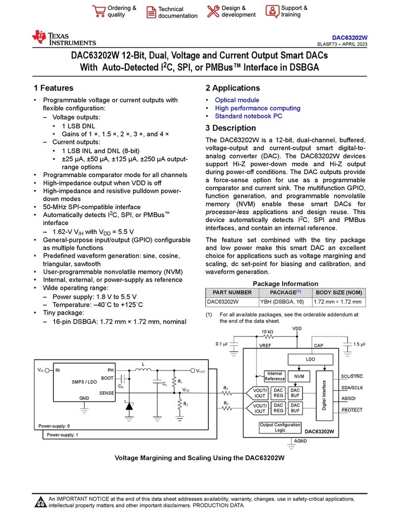
The THS1031 is a CMOS, low-power, 10-bit, 30 MSPS analog-to-digital converter (ADC) that can operate with
a supply range from 3 V to 5.5 V. The THS1031 has been designed to give circuit developers flexibility. The
analoginputtotheTHS1031canbeeithersingle-endedordifferential.Thisdevicehasabuilt-inclampamplifier
whoseclampinputlevelcanbedrivenfromanexternaldcsourceorfromaninternalhigh-precision10-bitdigital
clamp level programmable via an internal CLAMP register. A 3-bit PGA is included to maintain SNR for small
signals.TheTHS1031providesawideselectionofvoltagereferencestomatchtheuser’sdesignrequirements.
For more design flexibility, the internal reference can be bypassed to use an external reference to suit the dc
accuracy and temperature drift requirements of the application. The out-of-range output indicates any
out-of-range condition in THS1031’s input signal. The format of digital output can be coded in either unsigned
binary or 2s complement.
The speed, resolution, and single-supply operation of the THS1031 are suited to applications in set-top-box
(STB), video, multimedia, imaging, high-speed acquisition, and communications. The built-in clamp function
allowsdc restorationofvideo signaland issuitable forvideo applications.Thespeed andresolution ideallysuit
charge-couple device (CCD) input systems such as color scanners, digital copiers, digital cameras, and
camcorders.AwideinputvoltagerangebetweenREFBSandREFTSallowstheTHS1031tobeappliedinboth
imaging and communications systems.
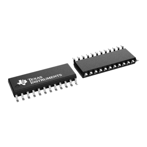
The THS1031C is characterized for operation from 0°C to 70°C, while the THS1031I is characterized for
operation from –40°C to 85°C.
AVAILABLE OPTIONS
PACKAGED DEVICES
A28-TSSOP (PW) 28-SOIC (DW)
0°C to 70°C THS1031CPW THS1031CDW
–40°C to 85°C THS1031IPW THS1031IDW
Copyright 2002, Texas Instruments Incorporated
PRODUCTION DATA information is current as of publication date.
Products conform to specifications per the terms of Texas Instruments
standard warranty. Production processing does not necessarily include
testing of all parameters.
Please be aware that an important notice concerning availability, standard warranty, and use in critical applications of
Texas Instruments semiconductor products and disclaimers thereto appears at the end of this data sheet.
1
2
3
4
5
6
7
8
9
10
11
12
13
14
28
27
26
25
24
23
22
21
20
19
18
17
16
15
AGND
DVDD
I/O0
I/O1
I/O2
I/O3
I/O4
I/O5
I/O6
I/O7
I/O8
I/O9
OVR
DGND
AVDD
AIN
VREF
REFBS
REFBF
MODE
REFTF
REFTS
CLAMPIN
CLAMP
REFSENSE
WR
OE
CLK
28-PIN TSSOP/SOIC PACKAGE
(TOP VIEW)
