Wolfson WM8940 User manual

w WM8940
Mono CODEC with Speaker Driver
WOLFSON MICROELECTRONICS plc
To receive regular email updates, sign up at http://www.wolfsonmicro.com/enews/
Production Data, Rev 4.2, April 2008
Copyright ©2008 Wolfson Microelectronics plc
DESCRIPTION
The WM8940 is a low power, high quality mono CODEC
designed for portable applications such as digital still cameras
or camcorders.
The device integrates support for a differential or single ended
mic, and includes drivers for speakers or headphone, and
mono line output. External component requirements are
reduced as no separate microphone or headphone amplifiers
are required.
Advanced Sigma Delta Converters are used along with digital
decimation and interpolation filters to give high quality audio at
sample rates from 8 to 48ks/s. A selectable high pass filter
and four fully-programmable notch filters are available in the
ADC path. An advanced mixed signal ALC function with noise
gate is provided, while readback of PGA gain during ALC
operation is supported. The digital audio interface supports A-
law and µ-law companding.
An on-chip PLL is provided to generate the required Master
Clock from an external reference clock. The PLL clock can
also be output if required elsewhere in the system.
The WM8940 operates at supply voltages from 2.5 to 3.6V,
although the digital supplies can operate at voltages down to
1.71V to save power. Different sections of the chip can also be
powered down under software control using the selectable two
or three wire control interface.
WM8940 is supplied in a very small 4x4mm QFN package,
offering high levels of functionality in minimum board area,
with high thermal performance.
FEATURES
•Mono CODEC:
•Audio sample rates:8, 11.025, 16, 22.05, 24, 32, 44.1, 48kHz
•DAC SNR 98dB, THD -84dB (‘A’-weighted @ 8 – 48ks/s)
•ADC SNR 94dB, THD -80dB (‘A’-weighted @ 8 – 48ks/s)
•On-chip Headphone/Speaker Driver
- 40mW output power into 16Ω
- BTL speaker drive 0.4W into 8Ω
•Additional MONO Line output
•Multiple analog or ‘Aux’ inputs, plus analog bypass path
•Mic Preamps:
•Differential or single end Microphone Interface
- Programmable preamp gain
- Pseudo differential inputs with common mode rejection
- Programmable ALC / Noise Gate in ADC path
•Low-noise bias supplied for electret microphones
OTHER FEATURES
•Digital Playback Limiter
•Programmable high pass filter (wind noise reduction)
•4 notch filters (narrowband noise suppression)
•On-chip PLL
•Low power, low voltage
- 2.5V to 3.6V (digital: 1.71V to 3.6V)
•4x4x0.9mm 24 lead QFN package
APPLICATIONS
•Digital still cameras and camcorders
•General purpose mono audio CODEC

WM8940 Production Data
w PD, Rev 4.2, April 2008
2
BLOCK DIAGRAM

Production Data WM8940
wPD, Rev 4.2, April 2008
3
TABLE OF CONTENTS
DESCRIPTION .......................................................................................................1
FEATURES.............................................................................................................1
APPLICATIONS .....................................................................................................1
BLOCK DIAGRAM.................................................................................................2
TABLE OF CONTENTS .........................................................................................3
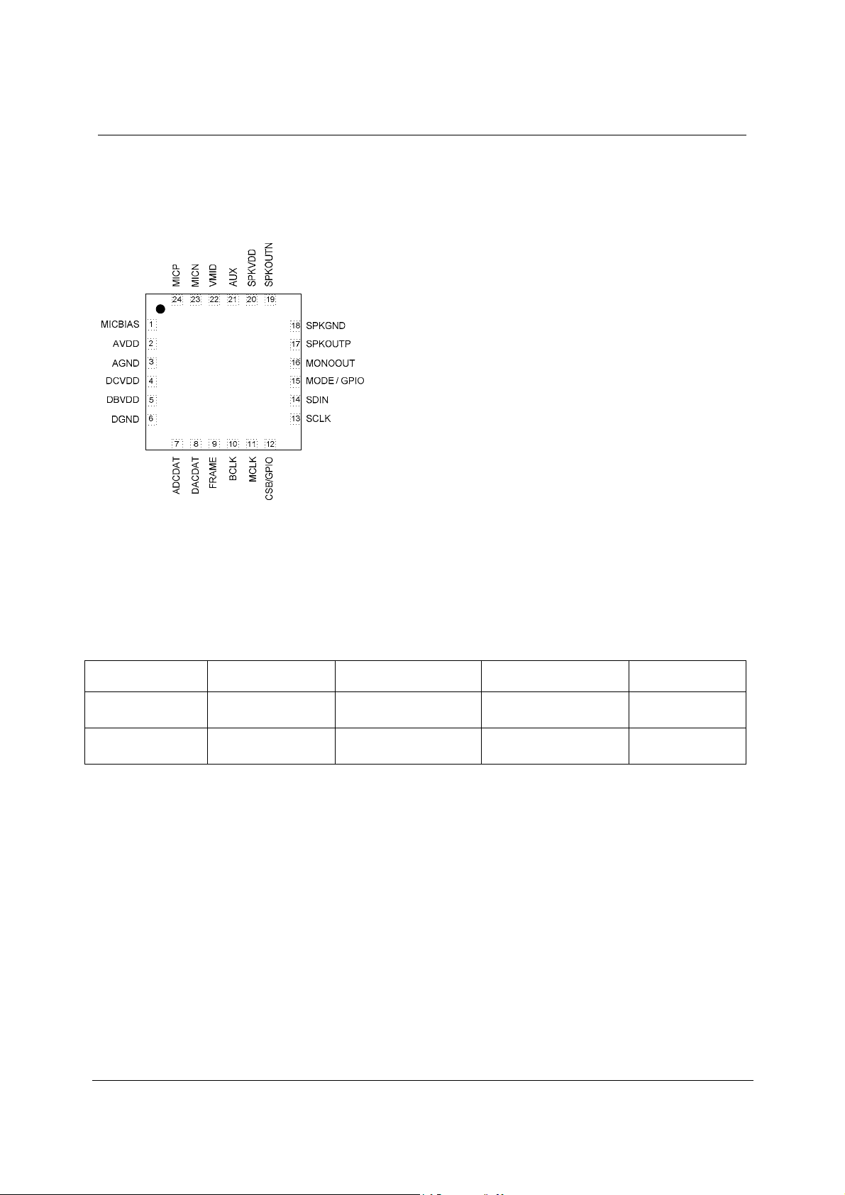
PIN CONFIGURATION...........................................................................................5
ORDERING INFORMATION ..................................................................................5
PIN DESCRIPTION ................................................................................................6
ABSOLUTE MAXIMUM RATINGS.........................................................................7
RECOMMENDED OPERATING CONDITIONS .....................................................7
ELECTRICAL CHARACTERISTICS ......................................................................8
TERMINOLOGY .......................................................................................................... 10
AUDIO PATHS OVERVIEW.................................................................................11
SIGNAL TIMING REQUIREMENTS.....................................................................13
SYSTEM CLOCK TIMING ........................................................................................... 13
AUDIO INTERFACE TIMING – MASTER MODE ........................................................ 13
AUDIO INTERFACE TIMING – SLAVE MODE............................................................ 14
CONTROL INTERFACE TIMING – 3-WIRE MODE .................................................... 15
CONTROL INTERFACE TIMING – 2-WIRE MODE .................................................... 16
DEVICE DESCRIPTION.......................................................................................17
INTRODUCTION......................................................................................................... 17
INPUT SIGNAL PATH ................................................................................................. 18
ANALOGUE TO DIGITAL CONVERTER (ADC).......................................................... 23
INPUT LIMITER / AUTOMATIC LEVEL CONTROL (ALC) .......................................... 28
OUTPUT SIGNAL PATH ............................................................................................. 41
ANALOGUE OUTPUTS............................................................................................... 45
OUTPUT SWITCH ...................................................................................................... 48
DIGITAL AUDIO INTERFACES................................................................................... 51
AUDIO SAMPLE RATES............................................................................................. 55
MASTER CLOCK AND PHASE LOCKED LOOP (PLL)............................................... 55
COMPANDING............................................................................................................ 58
GENERAL PURPOSE INPUT/OUTPUT...................................................................... 60
CONTROL INTERFACE.............................................................................................. 61
3-WIRE SERIAL CONTROL MODE ............................................................................ 62
READBACK IN 3-WIRE MODE ................................................................................... 62
2-WIRE SERIAL CONTROL MODE ............................................................................ 63
RESETTING THE CHIP .............................................................................................. 64
POWER SUPPLIES .................................................................................................... 64
POWER MANAGEMENT ............................................................................................ 66
POP MINIMISATION ................................................................................................... 67
REGISTER MAP...................................................................................................68
REGISTER BITS BY ADDRESS ................................................................................. 69
DIGITAL FILTER CHARACTERISTICS...............................................................80
TERMINOLOGY .......................................................................................................... 80
DAC FILTER RESPONSES......................................................................................... 81
ADC FILTER RESPONSES......................................................................................... 81
HIGHPASS FILTER..................................................................................................... 82
NOTCH FILTERS AND LOW PASS FILTER............................................................... 83

WM8940 Production Data
w PD, Rev 4.2, April 2008
4
NOTCH FILTER WORKED EXAMPLE........................................................................ 84
APPLICATIONS INFORMATION.........................................................................85
RECOMMENDED EXTERNAL COMPONENTS.......................................................... 85
PACKAGE DIAGRAM ..........................................................................................86
IMPORTANT NOTICE..........................................................................................87
ADDRESS ................................................................................................................... 87

Production Data WM8940
wPD, Rev 4.2, April 2008
5
PIN CONFIGURATION
TOP VIEW
ORDERING INFORMATION
ORDER CODE TEMPERATURE
RANGE PACKAGE MOISTURE SENSITIVITY
LEVEL PACKAGE BODY
TEMPERATURE
WM8940GEFL/V -25°C to +85°C
24-lead QFN (4x4x0.9mm)
(Pb-free)
MSL3 260oC
WM8940GEFL/RV -25°C to +85°C
24-lead QFN (4x4x0.9mm)
(Pb-free, tape and reel)
MSL3 260oC
Note:
Reel Quantity = 3,500

WM8940 Production Data
w PD, Rev 4.2, April 2008
6
PIN DESCRIPTION
PIN NAME TYPE DESCRIPTION
1 MICBIAS Analogue Output Microphone bias
2 AVDD Supply Analogue supply
3 AGND Supply Analogue ground
4 DCVDD Supply Digital Supply (Core)
5 DBVDD Supply Digital supply (Input/Output)
6 DGND Supply Digital ground
7 ADCDAT Digital Output ADC digital audio data output
8 DACDAT Digital Input DAC digital audio data input
9 FRAME Digital Input / Output DAC and ADC sample rate clock or frame synch
10 BCLK Digital Input / Output Digital audio port clock
11 MCLK Digital Input Master clock input
12 CSB/GPIO Digital Input / Output 3-Wire control interface chip select or GPIO pin.
13 SCLK Digital Input 3-Wire control interface clock Input / 2-Wire control interface clock
input
14 SDIN Digital Input / Output 3-Wire control interface data Input / 2-Wire control interface data input
15 MODE / GPIO Digital Input Control interface mode selection pin or GPIO pin.
16 MONOOUT Analogue Output Mono output
17 SPKOUTP Analogue Output Speaker output positive
18 SPKGND Supply Speaker ground
19 SPKOUTN Analogue Output Speaker output negative
20 SPKVDD Supply Speaker supply
21 AUX Analogue Input Auxiliary analogue input
22 VMID Reference Decoupling for midrail reference voltage
23 MICN Analogue Input Microphone negative input (common mode)
24 MICP Analogue Input Microphone positive input
Note:
1. It is recommended that the QFN ground paddle should be connected to analogue ground on the application PCB.
2. Refer to the application note WAN_0118 on “Guidelines on How to Use QFN Packages and Create Associated PCB
Footprints”

Production Data WM8940
wPD, Rev 4.2, April 2008
7
ABSOLUTE MAXIMUM RATINGS
Absolute Maximum Ratings are stress ratings only. Permanent damage to the device may be caused by continuously
operating at or beyond these limits. Device functional operating limits and guaranteed performance specifications are given
under Electrical Characteristics at the test conditions specified.
ESD Sensitive Device. This device is manufactured on a CMOS process. It is therefore generically susceptible to
damage from excessive static voltages. Proper ESD precautions must be taken during handling and storage of this
device.
Wolfson tests its package types according to IPC/JEDEC J-STD-020B for Moisture Sensitivity to determine acceptable storage
conditions prior to surface mount assembly. These levels are:
MSL1 = unlimited floor life at <30°C / 85% Relative Humidity. Not normally stored in moisture barrier bag.
MSL2 = out of bag storage for 1 year at <30°C / 60% Relative Humidity. Supplied in moisture barrier bag.
MSL3 = out of bag storage for 168 hours at <30°C / 60% Relative Humidity. Supplied in moisture barrier bag.
The Moisture Sensitivity Level for each package type is specified in Ordering Information.
CONDITION MIN MAX
DBVDD, DCVDD, AVDD, SPKVDD supply voltages -0.3V +4.2
Voltage range digital inputs DGND -0.3V DVDD +0.3V
Voltage range analogue inputs AGND -0.3V AVDD +0.3V
Operating temperature range, TA-25°C +85°C
Storage temperature prior to soldering 30°C max / 85% RH max
Storage temperature after soldering -65°C +150°C
Notes
1. Analogue and digital grounds must always be within 0.3V of each other.
2. All digital and analogue supplies are completely independent from each other.
RECOMMENDED OPERATING CONDITIONS
PARAMETER SYMBOL TEST CONDITIONS MIN TYP MAX UNIT
Digital supply range (Core) DCVDD 1.71 3.6 V
Digital supply range (Buffer) DBVDD 1.71 3.6 V
Analogue supplies range AVDD, SPKVDD12.5 3.6 V
Ground DGND,AGND, SPKGND 0 V
Notes
1. Analogue supply voltages must be ≥the digital supply voltages
2. DBVDD must be ≥DCVDD

WM8940 Production Data
w PD, Rev 4.2, April 2008
8
ELECTRICAL CHARACTERISTICS
Test Conditions
DCVDD = 1.8V, AVDD = DBVDD = 3.3V, SPKVDD =3.3V, TA = +25oC, 1kHz signal, fs = 48kHz, 24-bit audio data unless otherwise
stated.
PARAMETER SYMBOL TEST CONDITIONS MIN TYP MAX UNIT
Microphone Input PGA Inputs (MICN, MICP)
INPPGAVOL and PGABOOST = 0dB
Full-scale Input Signal Level – Single-
ended input via LIN/RIN 1
AVDD/3.3 Vrms
Full-scale Input Signal Level –
Pseudo-differential input 1,2
AVDD*0.7/
3.3
V
rms
Input PGA equivalent input noise INPPGAVOL = +35.25dB
No input signal
0 to 20kHz
76.5 dB
MICN input resistance INPPGAVOL = +35.25dB 2 kΩ
MICN input resistance INPPGAVOL = 0dB 58.5 kΩ
MICN input resistance INPPGAVOL = -12dB 97.5 kΩ
MICP input resistance All gain settings 124.5 kΩ
Input Capacitance All analogue input pins 10 pF
Maximum Input PGA Programmable
Gain
Gain adjusted by
INPPGAVOL
+33.25 +35.25 +37.25 dB
Minimum Input PGA Programmable
Gain
Gain adjusted by
INPPGAVOL
-14 -12 -10 dB
Programmable Gain Step Size Guaranteed monotonic 0.75 dB
Input PGA Mute Attenuation INPPGAMUTE 92 dB
Input Gain Boost PGABOOST= 0 0 dB
Input Gain Boost PGABOOST = 1 +20 dB
Auxiliary Analogue Inputs (AUX)
Full-scale Input Signal Level 2AVDD/3.3
Vrms
Input Resistance Input boost and mixer
enabled, at 0dB gain
20 kΩ
Input Capacitance All analogue Inputs 10 pF
Maximum Gain from AUX input PGA
mixers
Gain adjusted by
AUX2BOOSTVOL
+4.0 +6 +7.5
dB
Minimum Gain from AUX input PGA
mixers
Gain adjusted by
AUX2BOOSTVOL
-14 -12 -9
dB
AUX2BOOSTVOL step size Guaranteed monotonic 3 dB
Analogue to Digital Converter (ADC) - Input from MICN and MICP in differential configuration to input PGA
INPPGAVO, PGABOOST and ADCVOL = 0dB
Signal to Noise Ratio 3SNR
A-weighted
AVDD=3.3V
88 91 dB
Total Harmonic Distortion 4 THD
-1dBV Input
AVDD=3.3V
-80 -75 dB
Total Harmonic Distortion + Noise 5
THD+N -1dBV Input
AVDD=3.3V
-75 -68 dB
Channel Separation 6
1kHz full scale input signal 100 dBFS

Production Data WM8940
wPD, Rev 4.2, April 2008
9
Test Conditions
DCVDD = 1.8V, AVDD = DBVDD = 3.3V, SPKVDD =3.3V, TA = +25oC, 1kHz signal, fs = 48kHz, 24-bit audio data unless otherwise
stated.
PARAMETER SYMBOL TEST CONDITIONS MIN TYP MAX UNIT
Digital to Analogue Converter (DAC) to MONO Output with 10kΩ/ 50pF load and DACVOL 0dB
Full-scale output 1DACVOL = 0dB AVDD/3.3 Vrms
Signal to Noise Ratio 3 SNR A-weighted
AVDD=SPKVDD=3.3V
93 98 dB
Total Harmonic Distortion 4
THD 0dBFS input
AVDD=SPKVDD=3.3V
-80 -75 dBFS
Total Harmonic Distortion + Noise 5
THD+N 0dBFS input
AVDD=SPKVDD=3.3V
-78 -74 dBFS
Channel Separation 6
1kHz signal 100 dB
MICP and MICN input PGA to input boost stage into 10kΩ/ 50pF load on SPKOUTP and SPKOUTP
INPPGAVOL, PGABOOST = 0dB
Full-scale output voltage, 0dB gain SPKVDD/3.3 Vrms
Signal to Noise Ratio 3 SNR A-weighted
AVDD=SPKVDD=3.3V
94 99 dB
Total Harmonic Distortion 4
THD full-scale signal
AVDD=SPKVDD=3.3V
-90 -85 dBFS
Total Harmonic Distortion + Noise 5
THD+N full-scale signal
AVDD=SPKVDD=3.3V
-87 -82 dBFS
Channel Separation 6100 dB
DAC to Speaker Output (SPKOUTP, SPKOUTN with 8Ωbridge tied load) Bypass mode
Output Power Po Output power is closely correlated with THD see below
Total Harmonic Distortion 4THD Po=350mW, RL = 8Ω
SPKVDD=3.3V
0.03
-70
-60
%
dB
Signal to Noise Ratio 3SNR A-weighted
SPKVDD=3.3V
93.5 98 dB
Power Supply Rejection Ratio
(50Hz-22kHz)
PSRR RL = 8ΩBTL 50 dB
AUX In to Headphone Output (SPKOUTP, SPKOUTN with 16R resistive load to GND) Bypass mode
Signal to Noise Ratio 3SNR A-weighted
SPKVDD=3.3V
95 99 dB
Total Harmonic Distortion 4
THD Po=20mW, RL = 16Ω
SPKVDD=3.3V
0.02
-74
-67 %
dB
Microphone Bias
MBVSEL=0 0.9*AVDD V
Bias Voltage
MBVSEL=1 0.65*AVDD V
Bias Current Source for VMICBIAS within +/-3% 3 mA
Output Noise Voltage 1kHz to 20kHz 15 nV/√Hz
Digital Input / Output
Input HIGH Level VIH 0.7×
DBVDD
V
Input LOW Level VIL 0.3×DBVDD V
Output HIGH Level VOH I
OL=1mA 0.9×
DBVDD
V
Output LOW Level VOL I
OH-1 m A 0.1xDBVDD V
Input Capacitance All digital pins 10 pF

WM8940 Production Data
w PD, Rev 4.2, April 2008
10
TERMINOLOGY
1. Full-scale input and output levels scale in relation to AVDD or SPKVDD depending upon the input or output used. For
example, when AVDD = 3.3V, 0dBFS = 1Vrms (0dBV). When AVDD < 3.3V the absolute level of 0dBFS will decrease
with a linear relationship to AVDD.
2. Input level to RIP and LIP in differential configurations is limited to a maximum of -3dB or performance will be
reduced.
3. Signal-to-noise ratio (dB) – SNR is the difference in level between a reference full scale output signal and the device
output with no signal applied. This ratio is also called idle channel noise. (No Auto-zero or Automute function is
employed in achieving these results).
4. Total Harmonic Distortion (dB) – THD is the difference in level between a reference output signal and the first seven
harmonics of that signal. The reference output signal need not be at full scale amplitude; THD is typically measured
using an output power of 20mW into a 16ohm load, corresponding to a reference signal level of -5dB. However the
stated test conditions include input signal level, signal gain settings, output load characteristics and power supply
voltages To calculate the ratio, the fundamental frequency of the output signal is notched out and an RMS value of
the next seven harmonics is calculated.
5. Total Harmonic Distortion plus Noise (dB) – THD+N is the difference in level between a reference output signal and
the sum of the harmonics, wide-band noise and interference on the output signal. To calculate the ratio, the
fundamental frequency of the output signal is notched out and an RMS value of the total harmonics, wide-band noise
and interference is calculated.
6. Channel Separation (dB) – Also known as Cross-Talk. This is a measure of the amount one channel is isolated from
the other. Normally measured by sending a full scale signal down

Production Data WM8940
wPD, Rev 4.2, April 2008
11
AUDIO PATHS OVERVIEW
Digital Core
DACPOL
R10[0]
DAC
AVDD
AGND
VREF+
VREF-
DCVDD
DGND DAC2SPK
R50[0]
LOUT1VOL
R52[5:0]
SPKVDD
AGND
SPKOUTN
AVDD
SPKGND
MONOOUT
AVDD
AGND
MONO
Mixer
+
DCVDD
DGND
ADCPOL
R14[0]
ADC
AVDD
AGND
VREF+
VREF-
DCVDD
DGND
DBVDD
DGND
DCVDD
DGND
PLL
AVDD
AGND
HPF
Limiter
+
AVDD
AGND
PGA
Mixer
AUX2BOOSTVOL
R47[2:0]
VMID
MICP2INPPGA
R44[0]
ALC/
Limiter
AUX2SPK
R50[5]
BYP2SPK
R50[1]
DAC2MONO
R56[0]
AUX2MONO
R56[2]
BYPL2MONO
R56[1]
MONOMUTE
R56[6]
VMID16Ohm
min
8Ohmmin
(BTL
Speaker)
WM8940 Audio Signal Paths
Notch
Filter
MICP
MICN
DACDATADCDAT
SPKOUTP
OUT3BOOST
R49[3]
AVDD
AGND
SPEAKER
Mixer
+
MICN2INPPGA
R44[1]
AUX2INPPGA
R44[2]
Digital Audio
Interface
MONOATTN
R56[7]
SPKATTN
R54[8]
SPKMUTE
R54[6]
VMID
INPPGAMUTE
R45[6]
-K
AUX
-
+
INPPGAVOL
R45[5:0]
ALCSEL[1]
R32[8]
From
ALC
PGABOOST
R47[8]
AUXMODE
R44[3]
AUX2BOOSTVOL
R47[2:0]=000
MIC2BOOSTVOL
R47[6:4]
MIC2BOOSTVOL
R47[6:4]=000)
Differential/
Single-Ended
MIC
PGA

WM8940 Production Data
w PD, Rev 4.2, April 2008
12
POWER CONSUMPTION
Typical current consumption for various scenarios is shown below.
MODE AVDD
(3V3) MA SPKVDD
(3V3) MA
DCVDD
(1.8V)
MA
DBVDD
(1.8V)
UA
TOTAL
POWER
(MW)
Power OFF (No Clocks) 0.038 0 0 0.2 0.126
Sleep (VMID maintained, No Clocks) 0.190 0 0 0.2 0.627
Mono Record (MIC input, +20dB gain, 8kHz,
quiescent) SLAVE 4.1 0 0.3 11 14.3
Mono Record (MIC input, +20dB gain, 44.1kHz,
PLL, quiescent) MASTER 5.3 0 1.9 115 21.0
Mono 16ΩHeadphone Playback (0.1mW, 1kHz
sine wave, ac coupled) SLAVE 2.8 1.5 1.6 3.7 17.1
Mono 8ΩBTL speaker Playback (44.1kHz,
200mW, 1kHz sine wave) SLAVE 2.8 62 1.6 3.8 216.8
Mono 8ΩBTL speaker Playback (44.1kHz,
PLL, quiescent) MASTER 3.9 1.5 1.8 81 21.1
Table 1 Power Consumption
Note: Power consumption figures include any power dissipated in the load (e.g. in the headphone or speaker)

Production Data WM8940
wPD, Rev 4.2, April 2008
13
SIGNAL TIMING REQUIREMENTS
SYSTEM CLOCK TIMING
MCLK
t
MCLKL
t
MCLKH
t
MCLKY
Figure 1 System Clock Timing Requirements
Test Conditions
DCVDD=1.8V, DBVDD=AVDD=SPKVDD=3.3V, DGND=AGND=SPKGND=0V, TA = +25oC
PARAMETER SYMBOL CONDITIONS MIN TYP MAX UNIT
System Clock Timing Information
MCLK=SYSCLK (=256fs) 81.38 ns
MCLK cycle time TMCLKY
MCLK input to PLL Note 1 20 ns
MCLK duty cycle TMCLKDS 60:40 40:60
Note 1:
PLL pre-scaling and PLL N and K values should be set appropriately so that SYSCLK is no greater than 12.288MHz.
AUDIO INTERFACE TIMING – MASTER MODE
Figure 2 Digital Audio Data Timing – Master Mode (see Control Interface)

WM8940 Production Data
w PD, Rev 4.2, April 2008
14
Test Conditions
DCVDD=1.8V, DBVDD=AVDD=SPKVDD=3.3V, DGND=AGND=SPKGND=0V, TA=+25oC, Slave Mode, fs=48kHz, MCLK=256fs,
24-bit data, unless otherwise stated.
PARAMETER SYMBOL MIN TYP MAX UNIT
Audio Data Input Timing Information
FRAME propagation delay from BCLK falling edge tDL 10 ns
ADCDAT propagation delay from BCLK falling edge tDDA 15 ns
DACDAT setup time to BCLK rising edge tDST 10 ns
DACDAT hold time from BCLK rising edge tDHT 10 ns
AUDIO INTERFACE TIMING – SLAVE MODE
Figure 3 Digital Audio Data Timing – Slave Mode
Test Conditions
DCVDD=1.8V, DBVDD=AVDD=SPKVDD=3.3V, DGND=AGND=SPKGND=0V, TA=+25oC, Slave Mode, fs=48kHz, MCLK= 256fs,
24-bit data, unless otherwise stated.
PARAMETER SYMBOL MIN TYP MAX UNIT
Audio Data Input Timing Information
BCLK cycle time tBCY 81.38 ns
BCLK pulse width high tBCH 32.55 ns
BCLK pulse width low tBCL 32.55 ns
FRAME set-up time to BCLK rising edge tLRSU 10 ns
FRAME hold time from BCLK rising edge tLRH 10 ns
DACDAT hold time from BCLK rising edge tDH 10 ns
DACDAT set-up time to BCLK rising edge tDS 10 ns
ADCDAT propagation delay from BCLK falling edge tDD 15 ns
Note:
BCLK period should always be greater than or equal to MCLK period.

Production Data WM8940
wPD, Rev 4.2, April 2008
15
CONTROL INTERFACE TIMING – 3-WIRE MODE
Figure 4 Control Interface Timing – 3-Wire Serial Control Mode
Test Conditions
DCVDD = 1.8V, DBVDD = AVDD = SPKVDD = 3.3V, DGND = AGND = SPKGND = 0V, TA = +25oC, Slave Mode, fs = 48kHz,
MCLK = 256fs, 24-bit data, unless otherwise stated.
PARAMETER SYMBOL MIN TYP MAX UNIT
Program Register Input Information
SCLK rising edge to CSB rising edge tSCS 80 ns
SCLK pulse cycle time tSCY 200 ns
SCLK pulse width low tSCL 80 ns
SCLK pulse width high tSCH 80 ns
SDIN to SCLK set-up time tDSU 40 ns
SCLK to SDIN hold time tDHO 40 ns
CSB pulse width low tCSL 40 ns
CSB pulse width high tCSH 40 ns
CSB rising to SCLK rising tCSS 40 ns
Pulse width of spikes that will be suppressed tps 0 5 ns

WM8940 Production Data
w PD, Rev 4.2, April 2008
16
CONTROL INTERFACE TIMING – 2-WIRE MODE
SDIN
SCLK
t
3
t
1
t
6
t
2
t
7
t
5
t
4
t
3
t
8
t
9
Figure 5 Control Interface Timing – 2-Wire Serial Control Mode
Test Conditions
DCVDD=1.8V, DBVDD=AVDD=SPKVDD=3.3V, DGND=AGND=SPKGND=0V, TA = +25oC, Slave Mode, fs = 48kHz, MCLK =
256fs, 24-bit data, unless otherwise stated.
PARAMETER SYMBOL MIN TYP MAX UNIT
Program Register Input Information
SCLK Frequency 0 526 kHz
SCLK Low Pulse-Width t11.3 us
SCLK High Pulse-Width t2600 ns
Hold Time (Start Condition) t3600 ns
Setup Time (Start Condition) t4600 ns
Data Setup Time t5100 ns
SDIN, SCLK Rise Time t6300 ns
SDIN, SCLK Fall Time t7300 ns
Setup Time (Stop Condition) t8600 ns
Data Hold Time t9900 ns
Pulse width of spikes that will be suppressed tps 0 5 ns

Production Data WM8940
wPD, Rev 4.2, April 2008
17
DEVICE DESCRIPTION
INTRODUCTION
The WM8940 is a low power audio codec combining a high quality mono audio DAC and ADC, with
flexible line and microphone input and output processing. Applications for this device include digital
still cameras or camcorders with mono audio, record and playback capability.
FEATURES
The chip offers great flexibility in use, and so can support many different modes of operation as
follows:
MICROPHONE INPUTS
Two microphone inputs are provided, allowing for either a differential microphone input or a single
ended microphone to be connected. These inputs have a user programmable gain range of -12dB
to +35.25dB using internal resistors. After the input PGA stage comes a boost stage which can add
a further 20dB of gain. A microphone bias is output from the chip which can be used to bias the
microphones. The signal routing can be configured to allow manual adjustment of mic levels, or to
allow the ALC loop to control the level of mic signal that is transmitted.
Total gain through the microphone paths of up to +55.25dB can be selected.
PGA AND ALC OPERATION
A programmable gain amplifier is provided in the input path to the ADC. This may be used manually
or in conjunction with a mixed analogue/digital automatic level control (ALC) which keeps the
recording volume constant.
AUX INPUT
The device includes a mono input, AUX, that can be used as an input for warning tones (beep) etc.
The output from this circuit can be summed into the mono output and/or the speaker output paths,
so allowing for mixing of audio with ‘backing music’ etc as required. This path can also be summed
into the input in a flexible fashion, either to the input PGA as a second microphone input or as a line
input. The configuration of this circuit, with integrated on-chip resistors allows several analogue
signals to be summed into the single AUX input if required.
ADC
The mono ADC uses a multi-bit high-order over sampling architecture to deliver optimum
performance with low power consumption. Various sample rates are supported, from the 8ks/s rate
typically used in voice dictation, up to the 48ks/s rate used in high quality audio applications.
HI-FI DAC
The hi-fi DAC provides high quality audio playback suitable for all portable mono audio type
applications.
DIGITAL FILTERING
Advanced Sigma Delta Converters are used along with digital decimation and interpolation filters to
give high quality audio at sample rates from 8ks/s to 48ks/s.
Application specific digital filters are also available which help to reduce the effect of specific noise
sources such as wind noise or narrowband noise from other parts of the system. The filters include a
programmable ADC high pass filter and four fully programmable ADC notch filters.
OUTPUT MIXING AND VOLUME ADJUST
Flexible mixing is provided on the outputs of the device; a mixer is provided for the speaker outputs,
and an additional mono summer for the mono output. These mixers allow the output of the DAC, the
output of the ADC volume control and the Auxiliary input to be combined. The output volume can be
adjusted using the integrated digital volume control and there is additional analogue gain adjustment
capability on the speaker output.
AUDIO INTERFACES
The WM8940 has a standard audio interface, to support the transmission of audio data to and from
the chip. This interface is a 4 wire standard audio interface which supports a number of audio data
formats including I2S, DSP Mode, MSB-First, left justified and MSB-First, right justified, and can
operate in master or slave modes.

WM8940 Production Data
w PD, Rev 4.2, April 2008
18
CONTROL INTERFACES
To allow full software control over all its features, the WM8940 supports 2 or 3 wire control interface.
It is fully compatible and an ideal partner for a wide range of industry standard microprocessors,
controllers and DSPs. The selection between 2-wire mode and 3-wire mode is determined by the
state of the MODE pin. If MODE is high then 3-wire control mode is selected, if MODE is low then 2-
wire control mode is selected.
In 2 wire mode, only slave operation is supported, and the address of the device is fixed as 0011010.
CLOCKING SCHEMES
WM8940 offers the normal audio DAC clocking scheme operation, where 256fs MCLK is provided to
the DAC/ADC.
However, a PLL is also included which may be used to generate the internal master clock frequency
in the event that this is not available from the system controller. This PLL uses an input clock,
typically the 12MHz USB or ilink clock, to generate high quality audio clocks. If this PLL is not
required for generation of these clocks, it can be reconfigured to generate alternative clocks which
may then be output on the CLKOUT pin and used elsewhere in the system.
POWER CONTROL
The design of the WM8940 has given much attention to power consumption without compromising
performance. It operates at low supply voltages, and includes the facility to power off any unused
parts of the circuitry under software control.
As a power saving measure, ADC or DAC logic in the DSP core is held in its last enabled state when
the ADC or DAC is disabled. In order to prevent pops and clicks on restart due to residual data in
the filters, the master clock must remain for at least 64 input samples after the ADC or DAC has
been disabled.
INPUT SIGNAL PATH
The WM8940 has 3 flexible analogue inputs: two microphone inputs, and an auxiliary input. These
inputs can be used in a variety of ways. The input signal path before the ADC has a flexible PGA
block which then feeds into a gain boost/mixer stage.
MICROPHONE INPUTS
The WM8940 can accommodate a variety of microphone configurations including single ended and
differential inputs. The inputs through the MICN, MICP and optionally AUX pins are amplified through
the input PGA as shown in Figure 6 .
A pseudo differential input is the preferential configuration where the positive terminal of the input
PGA is connected to the MICP input pin by setting MICP2INPPGA=1. The microphone ground
should then be connected to MICN (when MICN2INPPGA=1) or optionally to AUX (when
AUX2INPPGA=1) input pins.
Alternatively a single ended microphone can be connected to the MICN input with MICN2INPPGA set
to 1. The non-inverting terminal of the input PGA should be connected internally to VMID by setting
MICP2INPPGA to 0.
In pseudo-differential mode the larger signal should be input to MICP and the smaller (e.g. noisy
ground connections) should be input to MICN.

Production Data WM8940
wPD, Rev 4.2, April 2008
19
Figure 6 Microphone Input PGA Circuit (switch positions shown are for differential mic
input)
REGISTER
ADDRESS BIT LABEL DEFAULT DESCRIPTION
2 AUX2INPPGA 0 Select AUX amplifier output as input PGA
signal source.
0=AUX not connected to input PGA
1=AUX connected to input PGA amplifier
negative terminal.
1 MICN2INPPGA 1 Connect MICN to input PGA negative
terminal.
0=MICN not connected to input PGA
1=MICN connected to input PGA amplifier
negative terminal.
R44
Input Control
0 MICP2INPPGA 0 Connect input PGA amplifier positive
terminal to MICP or VMID.
0 = input PGA amplifier positive terminal
connected to VMID
1 = input PGA amplifier positive terminal
connected to MICP through variable resistor
string
Table 2 Input Control
The input PGA is enabled by the IPPGAEN register bit.
REGISTER
ADDRESS BIT LABEL DEFAULT DESCRIPTION
R2
Power
Management 2
2 INPPGAEN 0 Input microphone PGA enable
0 = disabled
1 = enabled
Table 3 Input PGA Enable Control

WM8940 Production Data
w PD, Rev 4.2, April 2008
20
INPUT PGA VOLUME CONTROL
The input microphone PGA has a gain range from -12dB to +35.25dB in 0.75dB steps. The gain
from the MICN input to the PGA output and from the AUX amplifier to the PGA output are always
common and controlled by the register bits INPPGAVOL[5:0]. These register bits also affect the
MICP pin when MICP2INPPGA=1.
When the Automatic Level Control (ALC) is enabled the input PGA gain is then controlled
automatically and the INPPGAVOL bits should not be used.
REGISTER
ADDRESS BIT LABEL DEFAULT DESCRIPTION
7 INPPGAZC 0 Input PGA zero cross enable:
0=Update gain when gain register changes
1=Update gain on 1st zero cross after gain
register write.
6 INPPGAMUTE 1 Mute control for input PGA:
0=Input PGA not muted, normal operation
1=Input PGA muted (and disconnected from
the following input BOOST stage).
R45
Input PGA
volume
control
5:0 INPPGAVOL 010000 Input PGA volume
000000 = -12dB
000001 = -11.25db
.
010000 = 0dB
.
111111 = 35.25dB
R32
ALC control 1
8 ALCSEL 0 ALC function select:
0=ALC off (PGA gain set by INPPGAVOL
register bits)
1=ALC on (ALC controls PGA gain)
Table 4 Input PGA Volume Control
AUXILIARY INPUT
An auxiliary input circuit (Figure 7) is provided which consists of an amplifier which can be configured
either as an inverting buffer for a single input signal or as a mixer/summer for multiple inputs with the
use of external resistors. The circuit is enabled by the register bit AUXEN.
Figure 7 Auxiliary Input Circuit
This manual suits for next models
3
Table of contents
Other Wolfson Conference System manuals
Popular Conference System manuals by other brands

Aastra
Aastra Ascotel Office 45 operating instructions

Lucent Technologies
Lucent Technologies MERLIN LEGEND Release 6.1 System planning

DDMALL
DDMALL AGS-P-100-4K user manual

Elvex
Elvex Com-690 User instructions

Polycom
Polycom SoundStructure C8 Application note

Polycom
Polycom VBP 7301 Hardware installation guide