Wolfson WM8978 User manual

w WM8978
Stereo CODEC with Speaker Driver
WOLFSON MICROELECTRONICS plc
To receive regular email updates, sign up at http://www.wolfsonmicro.com/enews
Production Data, October 2011, Rev 4.5
Copyright 2011 Wolfson Microelectronics plc
DESCRIPTION
The WM8978 is a low power, high quality stereo CODEC
designed for portable applications such as multimedia phone,
digital still camera or digital camcorder.
The device integrates preamps for stereo differential mics, and
includes drivers for speakers, headphone and differential or
stereo line output. External component requirements are
reduced as no separate microphone or headphone amplifiers
are required.
Advanced on-chip digital signal processing includes a 5-band
equaliser, a mixed signal Automatic Level Control for the
microphone or line input through the ADC as well as a purely
digital limiter function for record or playback. Additional digital
filtering options are available in the ADC path, to cater for
application filtering such as ‘wind noise reduction’.
The WM8978 digital audio interface can operate as a master or
a slave. An internal PLL can generate all required audio clocks
for the CODEC from common reference clock frequencies, such
as 12MHz and 13MHz.
The WM8978 operates at analogue supply voltages from 2.5V to
3.3V, although the digital core can operate at voltages down to
1.71V to save power. The speaker outputs and OUT3/4 line
outputs can run from a 5V supply if increased output power is
required. Individual sections of the chip can also be powered
down under software control.
BLOCK DIAGRAM
FEATURES
Stereo CODEC:
DAC SNR 98dB, THD -84dB (‘A’ weighted @ 48kHz)
ADC SNR 95dB, THD -84dB (‘A’ weighted @ 48kHz)
On-chip Headphone Driver with ‘capless’ option
- 40mW per channel into 16/ 3.3V SPKVDD
1W output power into 8BTL speaker / 5V SPKVDD
- Capable of driving piezo speakers
- Stereo speaker drive configuration
Mic Preamps:
Stereo Differential or mono microphone Interfaces
- Programmable preamp gain
- Psuedo differential inputs with common mode
rejection
- Programmable ALC / Noise Gate in ADC path
Low-noise bias supplied for electret microphones
Other Features:
Enhanced 3-D function for improved stereo separation
Digital playback limiter
5-band Equaliser (record or playback)
Programmable ADC High Pass Filter (wind noise reduction)
Programmable ADC Notch Filter
Aux inputs for stereo analogue input signals or ‘beep’
On-chip PLL supporting 12, 13, 19.2MHz and other clocks
Support for 8, 11.025, 12, 16, 22.05, 24, 32, 44.1 and
48kHz sample rates
Low power, low voltage
- 2.5V to 3.6V (digital: 1.71V to 3.6V)
5x5mm 32-lead QFN package
APPLICATIONS
Stereo Camcorder or DSC
Multimedia Phone

WM8978 Production Data
w PD, Rev 4.5, October 2011
2
TABLE OF CONTENTS
DESCRIPTION....................................................................................................... 1
BLOCK DIAGRAM ................................................................................................ 1
FEATURES............................................................................................................ 1
APPLICATIONS..................................................................................................... 1
TABLE OF CONTENTS......................................................................................... 2
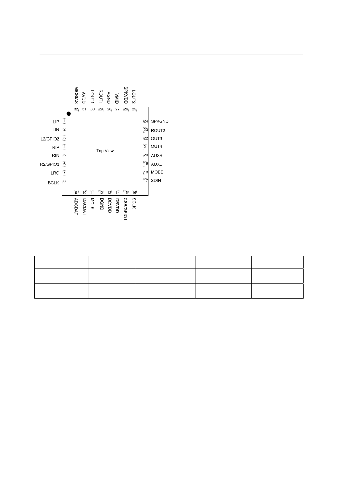
PIN CONFIGURATION.......................................................................................... 4
ORDERING INFORMATION.................................................................................. 4
PIN DESCRIPTION................................................................................................ 5
ABSOLUTE MAXIMUM RATINGS........................................................................ 6
RECOMMENDED OPERATING CONDITIONS..................................................... 6
ELECTRICAL CHARACTERISTICS ..................................................................... 7
TERMINOLOGY ............................................................................................................ 10
SPEAKER OUTPUT THD VERSUS POWER...................................................... 11
POWER CONSUMPTION.................................................................................... 12
AUDIO PATHS OVERVIEW ................................................................................ 14
SIGNAL TIMING REQUIREMENTS .................................................................... 15
SYSTEM CLOCK TIMING ............................................................................................. 15
AUDIO INTERFACE TIMING – MASTER MODE.......................................................... 15
AUDIO INTERFACE TIMING – SLAVE MODE ............................................................. 16
CONTROL INTERFACE TIMING – 3-WIRE MODE ...................................................... 17
CONTROL INTERFACE TIMING – 2-WIRE MODE ...................................................... 18
INTERNAL POWER ON RESET CIRCUIT.......................................................... 19
DEVICE DESCRIPTION ...................................................................................... 21
INTRODUCTION ........................................................................................................... 21
INPUT SIGNAL PATH ................................................................................................... 23
ANALOGUE TO DIGITAL CONVERTER (ADC) ........................................................... 30
INPUT LIMITER / AUTOMATIC LEVEL CONTROL (ALC)............................................ 36
OUTPUT SIGNAL PATH ............................................................................................... 47
3D STEREO ENHANCEMENT...................................................................................... 54
ANALOGUE OUTPUTS................................................................................................. 54
DIGITAL AUDIO INTERFACES..................................................................................... 70
AUDIO SAMPLE RATES............................................................................................... 75
MASTER CLOCK AND PHASE LOCKED LOOP (PLL) ................................................ 75
LOOPBACK ................................................................................................................... 77
COMPANDING .............................................................................................................. 77
GENERAL PURPOSE INPUT/OUTPUT........................................................................ 79
OUTPUT SWITCHING (JACK DETECT)....................................................................... 80
CONTROL INTERFACE................................................................................................ 82
RESETTING THE CHIP ................................................................................................ 83
POWER SUPPLIES....................................................................................................... 83
RECOMMENDED POWER UP/DOWN SEQUENCE.................................................... 83
POWER MANAGEMENT .............................................................................................. 88
REGISTER MAP.................................................................................................. 89
REGISTER BITS BY ADDRESS ................................................................................... 91
DIGITAL FILTER CHARACTERISTICS ............................................................ 108
TERMINOLOGY .......................................................................................................... 108
DAC FILTER RESPONSES ........................................................................................ 109
ADC FILTER RESPONSES ........................................................................................ 109
HIGHPASS FILTER..................................................................................................... 110

Production Data WM8978
wPD, Rev 4.5, October 2011
3
5-BAND EQUALISER .................................................................................................. 111
APPLICATION INFORMATION......................................................................... 115
RECOMMENDED EXTERNAL COMPONENTS ......................................................... 115
PACKAGE DIAGRAM ....................................................................................... 116
IMPORTANT NOTICE ....................................................................................... 117
ADDRESS ................................................................................................................... 117
REVISION HISTORY ......................................................................................... 118

WM8978 Production Data
w PD, Rev 4.5, October 2011
4
PIN CONFIGURATION
ORDERING INFORMATION
ORDER CODE TEMPERATURE
RANGE PACKAGE MOISTURE
SENSITIVITY LEVEL PEAK SOLDERING
TEMPERATURE
WM8978CGEFL/V -40C to +100C 32-lead QFN (5 x 5 mm)
(Pb-free)
MSL3 260oC
WM8978CGEFL/RV -40C to +100C 32-lead QFN (5 x 5 mm)
(Pb-free, tape and reel)
MSL3 260oC
Note:
Reel quantity = 3,500

Production Data WM8978
wPD, Rev 4.5, October 2011
5
PIN DESCRIPTION
PIN NAME TYPE DESCRIPTION
1 LIP Analogue input Left Mic Pre-amp positive input
2 LIN Analogue input Left Mic Pre-amp negative input
3 L2/GPIO2 Analogue input Left channel line input/secondary mic pre-amp positive input/GPIO2 pin
4 RIP Analogue input Right Mic Pre-amp positive input
5 RIN Analogue input Right Mic Pre-amp negative input
6 R2/GPIO3 Analogue input Right channel line input/secondary mic pre-amp positive input/GPIO3 pin
7 LRC
Digital Input / Output DAC and ADC Sample Rate Clock
8 BCLK
Digital Input / Output Digital Audio Port Clock
9 ADCDAT Digital Output ADC Digital Audio Data Output
10 DACDAT Digital Input DAC Digital Audio Data Input
11 MCLK Digital Input Master Clock Input
12 DGND Supply Digital ground
13 DCVDD Supply Digital core logic supply
14 DBVDD Supply Digital buffer (I/O) supply
15 CSB/GPIO1
Digital Input / Output 3-Wire Control Interface Chip Select / GPIO1 pin
16 SCLK Digital Input 3-Wire Control Interface Clock Input / 2-Wire Control Interface Clock
Input
17 SDIN
Digital Input / Output 3-Wire Control Interface Data Input / 2-Wire Control Interface Data Input
18 MODE Digital Input Control Interface Selection
19 AUXL Analogue input Left Auxillary input
20 AUXR Analogue input Right Auxillary input
21 OUT4 Analogue Output Buffered midrail Headphone pseudo-ground, or Right line output or MONO
mix output
22 OUT3 Analogue Output Buffered midrail Headphone pseudo-ground, or Left line output
23 ROUT2 Analogue Output Second right output, or BTL speaker driver positive output
24 SPKGND Supply Speaker ground (feeds speaker amp and OUT3/OUT4)
25 LOUT2 Analogue Output Second left output, or BTL speaker driver negative output
26 SPKVDD Supply Speaker supply (feed speaker amp only)
27 VMID Reference Decoupling for ADC and DAC reference voltage
28 AGND Supply Analogue ground (feeds ADC and DAC)
29 ROUT1 Analogue Output Headphone or Line Output Right
30 LOUT1 Analogue Output Headphone or Line Output Left
31 AVDD Supply Analogue supply (feeds ADC and DAC)
32 MICBIAS Analogue Output Microphone Bias
Note:
It is recommended that the QFN ground paddle should be connected to analogue ground on the application PCB. Refer to
the application note WAN_0118 on “Guidelines on How to Use QFN Packages and Create Associated PCB Footprints”.

WM8978 Production Data
w PD, Rev 4.5, October 2011
6
ABSOLUTE MAXIMUM RATINGS
Absolute Maximum Ratings are stress ratings only. Permanent damage to the device may be caused by continuously
operating at or beyond these limits. Device functional operating limits and guaranteed performance specifications are given
under Electrical Characteristics at the test conditions specified.
ESD Sensitive Device. This device is manufactured on a CMOS process. It is therefore generically susceptible
to damage from excessive static voltages. Proper ESD precautions must be taken during handling and storage
of this device.
Wolfson tests its package types according to IPC/JEDEC J-STD-020B for Moisture Sensitivity to determine acceptable storage
conditions prior to surface mount assembly. These levels are:
MSL1 = unlimited floor life at <30C / 85% Relative Humidity. Not normally stored in moisture barrier bag.
MSL2 = out of bag storage for 1 year at <30C / 60% Relative Humidity. Supplied in moisture barrier bag.
MSL3 = out of bag storage for 168 hours at <30C / 60% Relative Humidity. Supplied in moisture barrier bag.
The Moisture Sensitivity Level for each package type is specified in Ordering Information.
CONDITION MIN MAX
DBVDD, DCVDD, AVDD supply voltages -0.3V +4.5V
SPKVDD supply voltage -0.3V +7V
Voltage range digital inputs DGND -0.3V DVDD +0.3V
Voltage range analogue inputs AGND -0.3V AVDD +0.3V
Operating temperature range, TA-40C +100C
Storage temperature after soldering -65C +150C
Notes:
1. Analogue and digital grounds must always be within 0.3V of each other.
2. All digital and analogue supplies are completely independent from each other.
RECOMMENDED OPERATING CONDITIONS
PARAMETER SYMBOL TEST
CONDITIONS MIN TYP MAX UNIT
Digital supply range (Core) DCVDD 1.7113.6 V
Digital supply range (Buffer) DBVDD 1.7123.6 V
Analogue core supply range AVDD 2.5 3.6 V
Analogue output supply range SPKVDD 2.5 5.5 V
Ground DGND, AGND,
SPKGND
0 V
Notes:
1. When using the PLL, DCVDD must not be less than 1.9V.
2. DBVDD must be greater than or equal to DCVDD.
3. Analogue supplies have to be to digital supplies.
4. In non-boosted mode, SPKVDD should = AVDD, if boosted SPKVDD should be 1.5x AVDD.

Production Data WM8978
wPD, Rev 4.5, October 2011
7
ELECTRICAL CHARACTERISTICS
Test Conditions
DCVDD=1.8V, AVDD=DBVDD=SPKVDD= 3.3V, TA = +25oC, 1kHz signal, fs = 48kHz, 24-bit audio data unless otherwise stated.
PARAMETER SYMBOL TEST CONDITIONS MIN TYP MAX UNIT
Microphone Preamp Inputs (LIP, LIN, RIP, RIN, L2, R2)
Full-scale Input Signal Level –
note this changes in proportion
to AVDD (Note 1)
VINFS PGABOOST = 0dB
INPPGAVOL = 0dB
1.0
0
Vrms
dBV
Mic PGA equivalent input noise At 35.25dB
gain
0 to 20kHz 150 uV
Input resistance RMICIN Gain set to 35.25dB 1.6 k
RMICIN Gain set to 0dB 47 k
RMICIN Gain set to -12dB 75 k
RMICIP L/RIP2INPPGA = 1 94 k
CMICIN 10 pF
MIC Programmable Gain Amplifier (PGA)
Maximum Programmable Gain 35.25 dB
Minimum Programmable Gain -12 dB
Programmable Gain Step Size Guaranteed monotonic 0.75 dB
Mute Attenuation
120 dB
Selectable Input Gain Boost (0/+20dB)
Gain Boost on PGA input Boost disabled 0 dB
Boost enabled 20 dB
Maximum Gain from AUXL/R or
L/R2 input to boost/mixer
+6 dB
Minimum Gain from AUXL/R or
L/R2 input to boost/mixer
-12 dB
Gain step size to boost/mixer Guaranteed monotonic 3 dB
Auxiliary Analogue Inputs (AUXL, AUXR)
Full-scale Input Signal Level
(0dB) – note this changes in
proportion to AVDD
VINFS AVDD/3.3
0
Vrms
dBV
Input Resistance
(Note 2)
RAUXINLMIN Left Input boost and mixer
enabled, at max gain 4.3 k
RAUXINLTYP Left Input boost and mixer
enabled, at 0dB gain 8.6 k
RAUXINLMAX Left Input boost and mixer
enabled, at min gain 39.1 k
RAUXINRMIN Right Input boost, mixer and
beep enabled, at max gain 3 k
RAUXINRTYP Right Input boost, mixer and
beep enabled, at 0dB gain 6 k
RAUXINRMAX
R
ight Input boost, mixer and
beep enabled, at min gain 29 k
Input Capacitance CMICIN 10 pF

WM8978 Production Data
w PD, Rev 4.5, October 2011
8
Test Conditions
DCVDD=1.8V, AVDD=DBVDD=SPKVDD= 3.3V, TA = +25oC, 1kHz signal, fs = 48kHz, 24-bit audio data unless otherwise stated.
PARAMETER SYMBOL TEST CONDITIONS MIN TYP MAX UNIT
Automatic Level Control (ALC)
Target Record Level -22.5 -1.5 dB
Programmable gain -12 35.25
Gain Hold Time (Note 3,5) tHOLD MCLK = 12.288MHz
(Note 3)
0, 2.67, 5.33, 10.67, … , 43691
(time doubles with each step)
ms
Gain Ramp-Up (Decay) Time
(Note 4,5)
tDCY ALCMODE=0 (ALC),
MCLK=12.288MHz
(Note 3)
3.3, 6.6, 13.1, … , 3360
(time doubles with each step)
ms
ALCMODE=1 (limiter),
MCLK=12.288MHz
(Note 3)
0.73, 1.45, 2.91, … , 744
(time doubles with each step)
Gain Ramp-Down (Attack) Time
(Note 4,5)
tATK ALCMODE=0 (ALC),
MCLK=12.288MHz
(Note 3)
0.83, 1.66, 3.33, … , 852
(time doubles with each step)
ms
ALCMODE=1 (limiter),
MCLK=12.288MHz
(Note 3)
0.18, 0.36, 0.73, … , 186
(time doubles with each step)
Mute Attenuation 120 dB
Analogue to Digital Converter (ADC)
Signal to Noise Ratio (Note 6) SNR A-weighted, 0dB gain 85 95 dB
Total Harmonic Distortion
(Note 7)
THD -3dBFS input -84 -74 dB
Channel Separation (Note 9) 1kHz input signal 110 dB
Digital to Analogue Converter (DAC) to Line-Out (LOUT1, ROUT1 with 10k/ 50pF load)
Full-scale output PGA gains set to 0dB,
OUT34BOOST=0
AVDD/3.3 Vrms
PGA gains set to 0dB,
OUT34BOOST=1
1.5x
(AVDD/3.3)
Signal to Noise Ratio (Note 6) SNR A-weighted 90 98 dB
Total Harmonic Distortion
(Note 7)
THD RL = 10k
full-scale signal
-84 -76 dB
Channel Separation (Note 8) 1kHz signal 110 dB
Output Mixers (LMX1, RMX1)
Maximum PGA gain into mixer +6 dB
Minimum PGA gain into mixer -15 dB
PGA gain step into mixer Guaranteed monotonic 3 dB
Analogue Outputs (LOUT1, ROUT1, LOUT2, ROUT2)
Maximum Programmable Gain +6 dB
Minimum Programmable Gain -57 dB
Programmable Gain step size Guaranteed monotonic 1 dB
Mute attenuation 1kHz, full scale signal 85 dB
Headphone Output (LOUT1, ROUT1 with 32load)
0dB full scale output voltage AVDD/3.3 Vrms
Signal to Noise Ratio SNR A-weighted 102 dB
Total Harmonic Distortion THD RL = 16, Po=20mW
AVDD=3.3V
0.003
-92
%
dB
RL = 32 , Po=20mW
AVDD=3.3V
0.008
- 82
%
dB

Production Data WM8978
wPD, Rev 4.5, October 2011
9
Test Conditions
DCVDD=1.8V, AVDD=DBVDD=SPKVDD= 3.3V, TA = +25oC, 1kHz signal, fs = 48kHz, 24-bit audio data unless otherwise stated.
PARAMETER SYMBOL TEST CONDITIONS MIN TYP MAX UNIT
Speaker Output (LOUT2, ROUT2 with 8bridge tied load, INVROUT2=1)
Full scale output voltage, 0dB
gain. (Note 9)
SPKBOOST=0 SPKVDD/3.3 Vrms
SPKBOOST=1 (SPKVDD/3.3)*1.5
Output Power POOutput power is very closely correlated with THD; see below
Total Harmonic Distortion THD PO=200mW, RL = 8,
SPKVDD=3.3V
0.04
-68
%
dB
PO=320mW, RL = 8,
SPKVDD=3.3V
1.0
-40
%
dB
PO=500mW, RL = 8,
SPKVDD=5V
0.02
-74
%
dB
PO=860mW, RL = 8,
SPKVDD=5V
1.0
-40
%
dB
Signal to Noise Ratio SNR SPKVDD=3.3V,
RL = 8
90 dB
SPKVDD=5V,
RL = 8
90 dB
Power Supply Rejection Ratio
(50Hz-22kHz)
PSRR RL = 8BTL 80 dB
RL = 8BTL
SPKVDD=5V (boost)
69 dB
OUT3/OUT4 Outputs (with 10k/ 50pF load)
Full-scale output voltage, 0dB
gain (Note 10)
OUT3BOOST=0/
OUT4BOOST=0
SPKVDD/3.3 Vrms
OUT3BOOST=1
OUT4BOOST=1
(SPKVDD/3.3)*1.5 Vrms
Signal to Noise Ratio (Note 6) SNR A-weighted 98 dB
Total Harmonic Distortion
(Note 7)
THD RL = 10 k
full-scale signal
-84 dB
Channel Separation (Note 8) 1kHz signal 100 dB
Power Supply Rejection Ratio
(50Hz-22kHz)
PSRR RL = 10k52 dB
R
L = 10kSPKVDD=5V
(boost)
56 dB
Microphone Bias
Bias Voltage VMICBIAS MBVSEL=0 0.9*AVDD V
MBVSEL=1 0.65*AVDD V
Bias Current Source IMICBIAS 3 mA
Output Noise Voltage Vn 1K to 20kHz 15 nV/Hz
Digital Input / Output
Input HIGH Level VIH 0.7DBVDD V
Input LOW Level VIL 0.3DBVDD V
Output HIGH Level VOH I
OL=1mA 0.9DBVDD V
Output LOW Level VOL I
OH-1mA 0.1xDBVDD V
Input capacitance 10 pF
Input leakage 50 pA

WM8978 Production Data
w PD, Rev 4.5, October 2011
10
TERMINOLOGY
1. Input level to RIP and LIP is limited to a maximum of -3dB or THD+N performance will be reduced.
2. Note when BEEP path is not enabled then AUXL and AUXR have the same input impedances.
3. Hold Time is the length of time between a signal detected being too quiet and beginning to ramp up the gain. It does
not apply to ramping down the gain when the signal is too loud, which happens without a delay.
4. Ramp-up and Ramp-Down times are defined as the time it takes for the PGA to sweep across 90% of its gain range.
5. All hold, ramp-up and ramp-down times scale proportionally with MCLK
6. Signal-to-noise ratio (dB) – SNR is a measure of the difference in level between the full scale output and the output
with no signal applied. (No Auto-zero or Automute function is employed in achieving these results).
7. THD+N (dB) – THD+N is a ratio, of the rms values, of (Noise + Distortion)/Signal.
8. Channel Separation (dB) – Also known as Cross-Talk. This is a measure of the amount one channel is isolated from
the other. Measured by applying a full scale signal to one channel input and measuring the level of signal apparent at
the other channel output.
9. The maximum output voltage can be limited by the speaker power supply. If OUT3BOOST, OUT4BOOST or
SPKBOOST is set then SPKVDD should be 1.5xAVDD to prevent clipping taking place in the output stage (when PGA
gains are set to 0dB).

Production Data WM8978
wPD, Rev 4.5, October 2011
11
SPEAKER OUTPUT THD VERSUS POWER

WM8978 Production Data
w PD, Rev 4.5, October 2011
12
POWER CONSUMPTION
Typical current consumption for various scenarios is shown below.
MODE AVDD
(3.0V)
(mA)
DCVDD
(1.8V)
(mA)
DBVDD1
(3.0V)
(mA)
TOTAL
POWER
(mW)
Off 0.0430.0008 <0.0001 0.12
Sleep (VREF maintained, no clocks) 0.04 0.0008 <0.0001 0.12
Stereo Record (8kHz)24.1 1.0 0.001 14.1
Stereo 16HP Playback (44.1kHz, quiescent)23.3 6.2 0.004 21.1
Stereo 16HP Playback (44.1kHz, white noise)25.4 7.3 0.004 29.4
Stereo 16HP Playback (44.1kHz, sine wave)218 6.7 0.004 66.1
Notes:
1. DBVDD Current will increase with greater loading on digital I/O pins.
2. 5 Band EQ is enabled.
3. AVDD standby current will fall to nearer 15uA when thermal shutdown sensor is disabled.
Table 1 Power Consumption
ESTIMATING SUPPLY CURRENT
When either the DAC or ADC is enabled approximately 7mA will be drawn from DCVDD when
DCVDD=1.8V and fs=48kHz. When the PLL is enabled approximately 1.5mA additional current will
be drawn from DCVDD.
As a general rule, digital supply currents will scale in proportion to sample rates. Supply current for
analogue and digital blocks will also be lower at lower supply voltages.
Power consumed by the output drivers will depend greatly on the signal characteristics. A quiet
signal, or a signal with long periods of silence will consume less power than a signal which is
continuously loud.
Estimated supply current for the analogue blocks is shown in Table 2. Note that power dissipated in
the load is not shown.

Production Data WM8978
wPD, Rev 4.5, October 2011
13
REGISTER BIT AVDD CURRENT (mA)
AVDD=3.3V
BUFDCOPEN 0.1
OUT4MIXEN 0.2
OUT3MIXEN 0.2
PLLEN 1.2 (with clocks applied)
MICBEN 0.5
BIASEN 0.3
BUFIOEN 0.1
VMIDSEL 5K= >0.3, less than 0.1 for 75K300Ksettings
ROUT1EN 0.4
LOUT1EN 0.4
BOOSTENR 0.2
BOOSTENL 0.2
INPPGAENR 0.2
INPPGAENL 0.2
ADCENR 2.6 (x64, ADCOSR=0)
4.9 ( x128, ADCOSR=1)
ADCENL 2.6 (x64, ADCOSR=0)
4.9 ( x128, ADCOSR=1)
OUT4EN 0.2
OUT3EN 0.2
LOUT2EN 1mA from SPKVDD + 0.2mA from AVDD in 5V mode
ROUT2EN 1mA from SPKVDD + 0.2mA from AVDD in 5V mode
RMIXEN 0.2
LMIXEN 0.2
DACENR 1.8 (x64, DACOSR=0)
1.9 (x128, DACOSR=1)
DACENL 1.8 (x64, DACOSR=0)
1.9 (x128, DACOSR=1)
Table 2 AVDD Supply Current (AVDD=3.3V)

WM8978 Production Data
w PD, Rev 4.5, October 2011
14
AUDIO PATHS OVERVIEW

Production Data WM8978
wPD, Rev 4.5, October 2011
15
SIGNAL TIMING REQUIREMENTS
SYSTEM CLOCK TIMING
MCLK
t
MCLKL
t
MCLKH
t
MCLKY
Figure 1 System Clock Timing Requirements
Test Conditions
DCVDD=1.8V, DBVDD=AVDD=SPKVDD=3.3V, DGND=AGND=SPKGND=0V, TA = +25oC
PARAMETER SYMBOL CONDITIONS MIN TYP MAX UNIT
System Clock Timing Information
MCLK cycle time TMCLKY MCLK=SYSCLK (=256fs) 81.38 ns
MCLK input to PLL Note 1 20 ns
MCLK duty cycle TMCLKDS 60:40 40:60
Note 1:
PLL pre-scaling and PLL N and K values should be set appropriately so that SYSCLK is no greater than 12.288MHz.
AUDIO INTERFACE TIMING – MASTER MODE
Figure 2 Digital Audio Data Timing – Master Mode (see Control Interface)

WM8978 Production Data
w PD, Rev 4.5, October 2011
16
Test Conditions
DCVDD=1.8V, DBVDD=AVDD=SPKVDD=3.3V, DGND=AGND=SPKGND=0V, TA=+25oC, Master Mode, fs=48kHz,
MCLK=256fs, 24-bit data, unless otherwise stated.
PARAMETER SYMBOL MIN TYP MAX UNIT
Audio Data Input Timing Information
LRC propagation delay from BCLK falling edge tDL 10 ns
ADCDAT propagation delay from BCLK falling edge tDDA 10 ns
DACDAT setup time to BCLK rising edge tDST 10 ns
DACDAT hold time from BCLK rising edge tDHT 10 ns
AUDIO INTERFACE TIMING – SLAVE MODE
Figure 3 Digital Audio Data Timing – Slave Mode
Test Conditions
DCVDD=1.8V, DBVDD=AVDD=SPKVDD=3.3V, DGND=AGND=SPKGND=0V, TA=+25oC, Slave Mode, fs=48kHz,
MCLK= 256fs, 24-bit data, unless otherwise stated.
PARAMETER SYMBOL MIN TYP MAX UNIT
Audio Data Input Timing Information
BCLK cycle time tBCY 50 ns
BCLK pulse width high tBCH 20 ns
BCLK pulse width low tBCL 20 ns
LRC set-up time to BCLK rising edge tLRSU 10 ns
LRC hold time from BCLK rising edge tLRH 10 ns
DACDAT hold time from BCLK rising edge tDH 10 ns
DACDAT set-up time to BCLK rising edge tDs 10 ns
ADCDAT propagation delay from BCLK falling edge tDD 10 ns
Note:
BCLK period should always be greater than or equal to MCLK period.

Production Data WM8978
wPD, Rev 4.5, October 2011
17
CONTROL INTERFACE TIMING – 3-WIRE MODE
Figure 4 Control Interface Timing – 3-Wire Serial Control Mode
Test Conditions
DCVDD = 1.8V, DBVDD = AVDD = SPKVDD = 3.3V, DGND = AGND = SPKGND = 0V, TA=+25oC, Slave Mode, fs=48kHz,
MCLK = 256fs, 24-bit data, unless otherwise stated.
PARAMETER SYMBOL MIN TYP MAX UNIT
Program Register Input Information
SCLK rising edge to CSB rising edge tSCS 80 ns
SCLK pulse cycle time tSCY 200 ns
SCLK pulse width low tSCL 80 ns
SCLK pulse width high tSCH 80 ns
SDIN to SCLK set-up time tDSU 40 ns
SCLK to SDIN hold time tDHO 40 ns
CSB pulse width low tCSL 40 ns
CSB pulse width high tCSH 40 ns
CSB rising to SCLK rising tCSS 40 ns
Pulse width of spikes that will be suppressed tps 0 5 ns

WM8978 Production Data
w PD, Rev 4.5, October 2011
18
CONTROL INTERFACE TIMING – 2-WIRE MODE
SDIN
SCLK
t
3
t
1
t
6
t
2
t
7
t
5
t
4
t
3
t
8
t
9
Figure 5 Control Interface Timing – 2-Wire Serial Control Mode
Test Conditions
DCVDD=1.8V, DBVDD=AVDD=SPKVDD=3.3V, DGND=AGND=SPKGND=0V, TA=+25oC, Slave Mode, fs=48kHz,
MCLK = 256fs, 24-bit data, unless otherwise stated.
PARAMETER SYMBOL MIN TYP MAX UNIT
Program Register Input Information
SCLK Frequency 0 526 kHz
SCLK Low Pulse-Width t11.3 us
SCLK High Pulse-Width t2600 ns
Hold Time (Start Condition) t3600 ns
Setup Time (Start Condition) t4600 ns
Data Setup Time t5100 ns
SDIN, SCLK Rise Time t6300 ns
SDIN, SCLK Fall Time t7300 ns
Setup Time (Stop Condition) t8600 ns
Data Hold Time t9900 ns
Pulse width of spikes that will be suppressed tps 0 5 ns

Production Data WM8978
wPD, Rev 4.5, October 2011
19
INTERNAL POWER ON RESET CIRCUIT
Figure 6 Internal Power on Reset Circuit Schematic
The WM8978 includes an internal Power-On-Reset Circuit (POR), as shown in Figure 6, which is
used reset the digital logic into a default state after power up. The POR circuit is powered from AVDD
and monitors DVDD. It asserts PORB low if AVDD or DVDD is below a minimum threshold.
Figure 7 Typical Power up Sequence where AVDD is Powered before DVDD
Figure 7 shows a typical power-up sequence where AVDD comes up first. When AVDD goes above
the minimum threshold, Vpora, there is enough voltage for the circuit to guarantee PORB is asserted
low and the chip is held in reset. In this condition, all writes to the control interface are ignored. AVDD
will then ramp up to full supply level. Next DVDD rises to Vpord_on and PORB is released high and all
registers are in their default state and writes to the control interface may take place.
On power down, where AVDD falls first, PORB is asserted low whenever AVDD drops below the
minimum threshold Vpora_off.

WM8978 Production Data
w PD, Rev 4.5, October 2011
20
Figure 8 Typical Power up Sequence where DVDD is Powered before AVDD
Figure 8 shows a typical power-up sequence where DVDD comes up first. First it is assumed that
DVDD is already up to specified operating voltage. When AVDD goes above the minimum threshold,
Vpora, there is enough voltage for the circuit to guarantee PORB is asserted low and the chip is held in
reset. In this condition, all writes to the control interface are ignored. When AVDD rises to Vpora_on,
PORB is released high and all registers are in their default state and writes to the control interface
may take place.
On power down, where DVDD falls first, PORB is asserted low whenever DVDD drops below the
minimum threshold Vpord_off.
SYMBOL MIN TYP MAX UNIT
Vpora 0.4 0.6 0.8 V
Vpora_on 0.9 1.2 1.6 V
Vpora_off 0.4 0.6 0.8 V
Vpord_on 0.5 0.7 0.9 V
Vpord_off 0.4 0.6 0.8 V
Table 3 Typical POR operation (typical simulated values)
Notes:
1. If AVDD and DVDD suffer a brown-out (i.e. drop below the minimum recommended operating
level but do not go below Vpora_off or Vpord_off) then the chip will not reset and will resume normal
operation when the voltage is back to the recommended level again.
2. The chip will enter reset at power down when AVDD or DVDD falls below Vpora_off or Vpord_off. This
may be important if the supply is turned on and off frequently by a power management system.
3. The minimum tpor period is maintained even if DVDD and AVDD have zero rise time. This
specification is guaranteed by design rather than test.
Other manuals for WM8978
1
This manual suits for next models
2
Table of contents
Other Wolfson Conference System manuals
Popular Conference System manuals by other brands

Grandstream Networks
Grandstream Networks GVC3200RMT user guide

Polycom
Polycom HDX 4500 quick start guide

Unify
Unify OpenScape Business V2 How-to

AKE
AKE PowerCom plus Series Operating and installation instructions

TANDBERG
TANDBERG 1000 MXP user manual

Bosch
Bosch DCN Next Generation Installation and operation manual