Wolfson WM8758B User manual

w WM8758B
Stereo CODEC with Headphone Driver and Line Out
WOLFSON MICROELECTRONICS plc
To receive regular email updates, sign up at http://www.wolfsonmicro.com/enews
Production Data, January 2012, Rev 4.4
Copyright 2012 Wolfson Microelectronics plc
DESCRIPTION
The WM8758B is a low power, high quality stereo CODEC
designed for portable applications such as MP3 audio player.
The device integrates preamps for stereo differential mics, and
drivers for headphone and differential or stereo line output.
External component requirements are reduced as no separate
microphone or headphone amplifiers are required. Headphone
and line common feedback improves crosstalk and noise
performance.
Advanced on-chip digital signal processing includes a 5-band
equaliser, a mixed signal Automatic Level Control for the
microphone or line input through the ADC as well as a purely
digital limiter function for record or playback. Additional digital
filtering options are available in the ADC path, to cater for
application filtering such as ‘wind noise reduction’ and notch
filter.
The WM8758B digital audio interface can operate in master or
slave mode with an integrated PLL.
The WM8758B operates at analogue supply voltages from 2.5V
to 3.3V, although the digital supply voltages can operate at
voltages down to 1.71V to save power. Additional power
management control enables individual sections of the chip to
be powered down under software control.
BLOCK DIAGRAM
FEATURES
Stereo CODEC:
DAC SNR 100dB, THD -86dB (‘A’ weighted @ 48kHz)
ADC SNR 92.5dB, THD -75dB (‘A’ weighted @ 48kHz)
Headphone Driver
40mW per channel output power into 16/ 3.3V AVDD2
Line output
Mic Preamps:
Stereo Differential or mono microphone Interfaces
Programmable preamp gain
Psuedo differential inputs with common mode rejection
Programmable ALC / Noise Gate in ADC path
Low-noise bias supplied for electret microphones
Other Features:
Enhanced 3-D function for improved stereo separation
Digital playback limiter
5-band Equaliser (record or playback)
Programmable ADC High Pass Filter (wind noise reduction)
Programmable ADC Notch Filter
PLL supporting various clocks between 8MHz-50MHz
Sample rates supported (kHz): 8, 11.025, 12, 16, 22.05, 24,
32, 44.1, 48
Low power, low voltage
2.5V to 3.6V analogue supplies
1.71V to 3.6V digital supplies
5x5mm 32-lead QFN package
APPLICATIONS
Portable audio player

WM8758B Production Data
w PD, Rev 4.4, January 2012
2
TABLE OF CONTENTS
DESCRIPTION....................................................................................................... 1
BLOCK DIAGRAM ................................................................................................ 1
FEATURES............................................................................................................ 1
APPLICATIONS..................................................................................................... 1
TABLE OF CONTENTS......................................................................................... 2
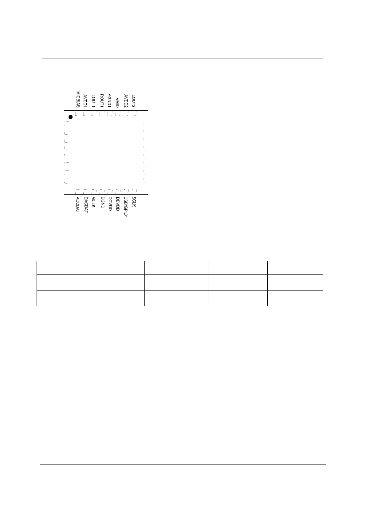
PIN CONFIGURATION .......................................................................................... 4
ORDERING INFORMATION.................................................................................. 4
PIN DESCRIPTION................................................................................................ 5
RECOMMENDED OPERATING CONDITIONS..................................................... 6
ELECTRICAL CHARACTERISTICS ..................................................................... 7
TERMINOLOGY ............................................................................................................ 12
HEADPHONE OUTPUT PERFORMANCE.......................................................... 13
POWER CONSUMPTION.................................................................................... 14
AUDIO PATHS OVERVIEW ................................................................................ 15
SIGNAL TIMING REQUIREMENTS .................................................................... 16
SYSTEM CLOCK TIMING ............................................................................................. 16
AUDIO INTERFACE TIMING – MASTER MODE.......................................................... 16
AUDIO INTERFACE TIMING – SLAVE MODE ............................................................. 17
CONTROL INTERFACE TIMING – 3-WIRE MODE ...................................................... 18
CONTROL INTERFACE TIMING – 2-WIRE MODE ...................................................... 19
INTERNAL POWER ON RESET CIRCUIT.......................................................... 20
RECOMMENDED POWER UP/DOWN SEQUENCE.................................................... 22
DEVICE DESCRIPTION ...................................................................................... 25
INTRODUCTION ........................................................................................................... 25
INPUT SIGNAL PATH ................................................................................................... 26
ANALOGUE TO DIGITAL CONVERTER (ADC) ........................................................... 33
INPUT LIMITER / AUTOMATIC LEVEL CONTROL (ALC)............................................ 37
OUTPUT SIGNAL PATH ............................................................................................... 42
3D STEREO ENHANCEMENT...................................................................................... 49
ANALOGUE OUTPUTS................................................................................................. 49
DIGITAL AUDIO INTERFACES..................................................................................... 61
AUDIO SAMPLE RATES............................................................................................... 68
MASTER CLOCK AND PHASE LOCKED LOOP (PLL) ................................................ 68
GENERAL PURPOSE INPUT/OUTPUT........................................................................ 70
OUTPUT SWITCHING (JACK DETECT)....................................................................... 72
CONTROL INTERFACE................................................................................................ 73
RESETTING THE CHIP ................................................................................................ 74
POWER SUPPLIES....................................................................................................... 75
POWER MANAGEMENT .............................................................................................. 75
POP MINIMISATION ..................................................................................................... 77
REGISTER MAP .................................................................................................. 78
DIGITAL FILTER CHARACTERISTICS .............................................................. 80
TERMINOLOGY ............................................................................................................ 80
DAC FILTER RESPONSES .......................................................................................... 81
ADC FILTER RESPONSES .......................................................................................... 81
HIGHPASS FILTER....................................................................................................... 82
5-BAND EQUALISER .................................................................................................... 83

Production Data WM8758B
wPD, Rev 4.4, January 2012
3
APPLICATIONS INFORMATION ........................................................................ 87
RECOMMENDED EXTERNAL COMPONENTS ........................................................... 87
PACKAGE DIAGRAM ......................................................................................... 88
IMPORTANT NOTICE ......................................................................................... 89
ADDRESS: .................................................................................................................... 89

WM8758B Production Data
w PD, Rev 4.4, January 2012
4
PIN CONFIGURATION
1
2
3
4
5
6
7
8
24
23
22
21
20
19
18
17
161514131211109
2526272829303132
TOP VIEW
R2/GPIO3
RIN
LIN
RIP
L2/GPIO2
LIP
LRC MODE
OUT4
HP_COM
LINE_COM
OUT3
ROUT2
SDIN
BCLK
AGND2
ORDERING INFORMATION
ORDER CODE TEMPERATURE
RANGE
PACKAGE MOISTURE
SENSITIVITY LEVEL
PEAK SOLDERING
TEMPERATURE
WM8758CBGEFL/V -40C to +85C 32-lead QFN (5 x 5 mm)
(Pb-free)
MSL3 260oC
WM8758CBGEFL/RV -40C to +85C 32-lead QFN (5 x 5 mm)
(Pb-free, tape and reel)
MSL3 260oC
Note:
Reel quantity = 3,500

Production Data WM8758B
wPD, Rev 4.4, January 2012
5
PIN DESCRIPTION
PIN NAME TYPE DESCRIPTION
1 LIP Analogue Input Left MIC pre-amp positive input
2 LIN Analogue Input Left MIC pre-amp negative input
3 L2/GPIO2 Analogue Input Left channel line input/secondary mic pre-amp positive input/GPIO2 pin
4 RIP Analogue Input Right MIC pre-amp positive input
5 RIN Analogue Input Right MIC pre-amp negative input
6 R2/GPIO3 Analogue Input Right channel line input/secondary mic pre-amp positive input/GPIO3 pin
7 LRC
Digital Input / Output DAC and ADC sample rate clock
8 BCLK
Digital Input / Output Digital audio bit clock
9 ADCDAT Digital Output ADC digital audio data output
10 DACDAT Digital Input DAC digital audio data input
11 MCLK Digital Input Master clock input
12 DGND Supply Digital ground
13 DCVDD Supply Digital core logic supply
14 DBVDD Supply Digital buffer (I/O) supply
15 CSB/GPIO1
Digital Input / Output 3-Wire control interface chip select / GPIO1 pin
16 SCLK Digital Input 3-Wire control interface clock input / 2-wire control interface clock input
17 SDIN
Digital Input / Output 3-Wire control interface data input / 2-Wire control interface data input
18 MODE Digital Input Control interface selection
19 HP_COM Analogue Input Headphone ground common feedback input
20 LINE_COM Analogue Input Line out ground common feedback input
21 OUT4 Analogue Output Right line output / mono mix output
22 OUT3 Analogue Output Left line output / mono mix output
23 ROUT2 Analogue Output Line output right 2
24 AGND2 Supply Analogue ground (return path for ROUT2/LOUT2)
25 LOUT2 Analogue Output Line output left 2
26 AVDD2 Supply Analogue supply (supply for output amplifiers ROUT2/LOUT2)
27 VMID Reference Decoupling for ADC and DAC reference voltage
28 AGND1 Supply Analogue ground (return path for all input amplifiers, PLL, ADC and
DAC, internal bias circuits, output amplifiers LOUT1, ROUT1 and
OUT3/OUT4 on AVDD1 AGND1)
29 ROUT1 Analogue Output Line or headphone output right 1
30 LOUT1 Analogue Output Line or headphone output left 1
31 AVDD1 Supply Analogue supply (feeds all input amplifiers, PLL, ADC and DAC, internal
bias circuits, output amplifiers LOUT1, ROUT1))
32 MICBIAS Analogue Output Microphone bias
Note:
It is recommended that the QFN ground paddle should be connected to analogue ground on the application PCB.

WM8758B Production Data
w PD, Rev 4.4, January 2012
6
ABSOLUTE MAXIMUM RATINGS
Absolute Maximum Ratings are stress ratings only. Permanent damage to the device may be caused by continuously
operating at or beyond these limits. Device functional operating limits and guaranteed performance specifications are given
under Electrical Characteristics at the test conditions specified.
ESD Sensitive Device. This device is manufactured on a CMOS process. It is therefore generically susceptible
to damage from excessive static voltages. Proper ESD precautions must be taken during handling and storage
of this device.
Wolfson tests its package types according to IPC/JEDEC J-STD-020B for Moisture Sensitivity to determine acceptable storage
conditions prior to surface mount assembly. These levels are:
MSL1 = unlimited floor life at <30C / 85% Relative Humidity. Not normally stored in moisture barrier bag.
MSL2 = out of bag storage for 1 year at <30C / 60% Relative Humidity. Supplied in moisture barrier bag.
MSL3 = out of bag storage for 168 hours at <30C / 60% Relative Humidity. Supplied in moisture barrier bag.
The Moisture Sensitivity Level for each package type is specified in Ordering Information.
CONDITION MIN MAX
DBVDD, DCVDD, AVDD1, AVDD2 supply voltages -0.3V +3.63V
Voltage range digital inputs DGND -0.3V DVDD +0.3V
Voltage range analogue inputs AGND1 -0.3V AVDD1 +0.3V
Storage temperature prior to soldering 30C max / 85% RH max
Storage temperature after soldering -65C +150C
Notes
1. Analogue and digital grounds must always be within 0.3V of each other.
2. All digital and analogue supplies are internally independent (i.e. not connected).
3. Analogue supply voltages should not be less than digital supply voltages.
4. DBVDD must be greater than or equal to DCVDD.
RECOMMENDED OPERATING CONDITIONS
PARAMETER SYMBOL TEST
CONDITIONS
MIN TYP MAX UNIT
Digital supply range (Core) DCVDD 1.711,2 1.8 3.6 V
Digital supply range (Buffer) DBVDD 1.71 3.3 3.6 V
Analogue supply range AVDD1, AVDD2 2.513.3 3.6 V
Ground DGND, AGND1, AGND2 0 V
Notes
1. Analogue supply voltages must not be less than digital supply voltages.
2. DBVDD must be greater than or equal to DCVDD.

Production Data WM8758B
wPD, Rev 4.4, January 2012
7
ELECTRICAL CHARACTERISTICS
Test Conditions
DCVDD=1.8V, AVDD1=AVDD2=3.0V, DBVDD=3.3V, TA = +25oC, 1kHz signal, fs = 48kHz, 24-bit audio data unless otherwise
stated.
PARAMETER SYMBOL TEST CONDITIONS MIN TYP MAX UNIT
Microphone Preamp Inputs (LIP, LIN, RIP, RIN, L2, R2)
Full-scale Input Signal Level –
Single-ended input via LIN/RIN
VINFS PGABOOST = 0dB
INPPGAVOL = 0dB
AVDD1/3.3 Vrms
Full-scale Input Signal Level –
Pseudo-differential input
VINFS PGABOOST = 0dB
INPPGAVOL = 0dB
AVDD1*0.7/
3.3
Vrms
Mic PGA equivalent input noise At 35.25dB
gain
0 to 20kHz 150 uV
Input resistance (LIN, RIN) RMICIN Gain set to 35.25dB 1.6 k
Input resistance (LIN, RIN) RMICIN Gain set to 0dB 46 k
Input resistance (LIN, RIN) RMICIN Gain set to -12dB 71 k
Input resistance (LIP, RIP) RMICIP 90 k
Input resistance (L2, R2) RL2R2 L/RIP2INPPGA = 1,
L/R2_2BOOSTVOL = 000
90 k
Input resistance (L2, R2) RL2R2 L/RIP2INPPGA = 0, Gain set
to 6dB
11 k
Input resistance (L2, R2) RL2R2 L/RIP2INPPGA = 0,
Gain set to 0dB
22 k
Input resistance (L2, R2) RL2R2 L/RIP2INPPGA = 0,
Gain set to -12dB
60 k
Input Capacitance CMICIN 10 pF
Maximum Programmable Gain +35.25 dB
Minimum Programmable Gain -12 dB
Programmable Gain Step Size Guaranteed monotonic 0.75 dB
MIC Mute Attenuation INPPGAMUTEL/R=1 100 dB
MIC Gain Boost PGABOOSTL/R=0 0 dB
PGABOOSTL/R=1 20 dB
L2, R2 Line Input Programmable Gain
Maximum Gain from L/R2 input
to boost/mixer
Gain adjusted by
L2_2BOOSTVOL
R2_2BOOSTVOL
+6 dB
Minimum Gain from L/R2 input
to boost/mixer
Gain adjusted by
L2_2BOOSTVOL
R2_2BOOSTVOL
-12 dB
L2/R2 boost step size Guaranteed monotonic 3 dB
L2/R2 Mute attenuation 100 dB
OUT4 to Left or Right Input Boost Record Path
Maximum Gain +6 dB
Minimum Gain -12 dB
Gain step size Guaranteed monotonic 3 dB
Mute attenuation 100 dB
Automatic Level Control (ALC)
Target Record Level -22.5 -1.5 dB
Programmable gain -12 35.25

WM8758B Production Data
w PD, Rev 4.4, January 2012
8
Test Conditions
DCVDD=1.8V, AVDD1=AVDD2=3.0V, DBVDD=3.3V, TA = +25oC, 1kHz signal, fs = 48kHz, 24-bit audio data unless otherwise
stated.
PARAMETER SYMBOL TEST CONDITIONS MIN TYP MAX UNIT
Analogue to Digital Converter (ADC) - Input from LIN/P and RIN/P, PGA and boost gains=0dB
Signal to Noise Ratio (Note 5,6) SNR A-weighted
AVDD1=AVDD2=3.0V
92.5 dB
A-weighted
AVDD1=AVDD2=2.5V
91.5 dB
22Hz to 20kHz
AVDD1=AVDD2=3.0V
90 dB
22Hz to 20kHz
AVDD1=AVDD2=2.5V
90 dB
Total Harmonic Distortion
(Note 7)
THD -12dBFS Input
AVDD1=AVDD2=3.0V
-75 dB
-12dBFS Input
AVDD1=AVDD2=2.5V
-75 dB
Total Harmonic Distortion + Noise
(Note 7)
THD+N -12dBFS Input
AVDD1=AVDD2=3.0V
-72 dB
-12dBFS Input
AVDD1=AVDD2=2.5V
-72 dB
Channel Separation (Note 8) 1kHz full scale input signal 100 dB
Analogue to Digital Converter (ADC) - Input from L2, R2
Signal to Noise Ratio (Note 5,6) SNR A-weighted
AVDD1=AVDD2=3.0V
85 92.5 dB
A-weighted
AVDD1=AVDD2=2.5V
92.5 dB
22Hz to 20kHz
AVDD1=AVDD2=3.0V
90 dB
22Hz to 20kHz
AVDD1=AVDD2=2.5V
90 dB
Total Harmonic Distortion
(Note 7)
THD -3dBFS Input
AVDD1=AVDD2=3.0V
-83 -75 dB
-3dBFS Input
AVDD1=AVDD2=2.5V
-66 dB
Total Harmonic Distortion + Noise
(Note 7)
THD+N -3dBFS Input
AVDD1=AVDD2=3.0V
-81 -70 dB
-3dBFS Input
AVDD1=AVDD2=2.5V
-65 dB
Channel Separation (Note 8) 1kHz input signal 100 dB

Production Data WM8758B
wPD, Rev 4.4, January 2012
9
Test Conditions
DCVDD=1.8V, AVDD1=AVDD2=3.0V, DBVDD=3.3V, TA = +25oC, 1kHz signal, fs = 48kHz, 24-bit audio data unless otherwise
stated.
PARAMETER SYMBOL TEST CONDITIONS MIN TYP MAX UNIT
DAC to L/R Mix to Line-Out (LOUT1/ROUT1 with 10k/ 50pF load, analogue volume controls set to 0dB)
Full-scale output PGA gains set to 0dB AVDD1/3.3 Vrms
Signal to Noise Ratio (Note 5,6) SNR A-weighted
AVDD1=AVDD2=3.0V
100 dB
A-weighted
AVDD1=AVDD2=2.5V
96 dB
22Hz to 20kHz
AVDD1=AVDD2=3.0V
95.5 dB
22Hz to 20kHz
AVDD1=AVDD2=2.5V
93.5 dB
Total Harmonic Distortion
(Note 7)
THD full-scale signal
AVDD1=AVDD2=3.0V
-86 dB
full-scale signal
AVDD1=AVDD2=2.5V
-86 dB
Total Harmonic Distortion + Noise
(Note 7)
THD+N full-scale signal
AVDD1=AVDD2=3.0V
-84 dB
full-scale signal
AVDD1=AVDD2=2.5V
-84 dB
Channel Separation (Note 8) 1kHz signal 100 dB
Ground noise rejection 10mV, 20kHz noise on
HPCOM, HPCOM enabled
40 dB
DAC to L/R Mix to Line-Out (LOUT2/ROUT2 with 10k/ 50pF load, analogue volume controls set to 0dB)
Full-scale output PGA gains set to 0dB AVDD1/3.3 Vrms
Signal to Noise Ratio (Note 5,6) SNR A-weighted
AVDD1=AVDD2=3.0V
95 100 dB
A-weighted
AVDD1=AVDD2=2.5V
96 dB
22Hz to 20kHz
AVDD1=AVDD2=3.0V
95.5 dB
22Hz to 20kHz
AVDD1=AVDD2=2.5V
93.5 dB
Total Harmonic Distortion
(Note 7)
THD full-scale signal
AVDD1=AVDD2=3.0V
-87 -80 dB
full-scale signal
AVDD1=AVDD2=2.5V
-82 dB
Total Harmonic Distortion + Noise
(Note 7)
THD+N full-scale signal
AVDD1=AVDD2=3.0V
-85 -75 dB
full-scale signal
AVDD1=AVDD2=2.5V
-80 dB
Channel Separation (Note 8) 1kHz signal 100 dB
Ground noise rejection 10mV, 20kHz noise on
LCOM, LCOM enabled
40 dB

WM8758B Production Data
w PD, Rev 4.4, January 2012
10
Test Conditions
DCVDD=1.8V, AVDD1=AVDD2=3.0V, DBVDD=3.3V, TA = +25oC, 1kHz signal, fs = 48kHz, 24-bit audio data unless otherwise
stated.
PARAMETER SYMBOL TEST CONDITIONS MIN TYP MAX UNIT
DAC to L/R Mix to Headphone (LOUT1/ROUT1, analogue volume controls set to 0dB)
Full-scale output PGA gains set to 0dB AVDD1/3.3 Vrms
Signal to Noise Ratio (Note 5,6) SNR A-weighted 100 dB
22Hz to 20kHz 95.5 dB
Total Harmonic Distortion
(Note 7)
THD Po = 20mW
RL=16Ω
-75 dB
Po = 20mW
RL=32Ω
-79 dB
Total Harmonic Distortion + Noise
(Note 7)
THD+N Po = 20mW
RL=16Ω
-75 dB
Po = 20mW
RL=32Ω
-79 dB
Channel Separation (Note 8) 1kHz signal 100 dB
Ground noise rejection 10mV, 20kHz noise on
HPCOM, HPCOM enabled
40 dB
DAC to L/R Mix to Headphone (LOUT2/ROUT2, analogue volume controls set to 0dB)
Full-scale output PGA gains set to 0dB AVDD1/3.3 Vrms
Signal to Noise Ratio (Note 5,6) SNR A-weighted 90 97 dB
22Hz to 20kHz 95.5 dB
Total Harmonic Distortion
(Note 7)
THD Po = 20mW
RL=16Ω
-79 dB
Po = 20mW
RL=32Ω
-82 dB
Channel Separation (Note 8) 1kHz signal 100 dB
Ground noise rejection 10mV, 20kHz noise on
LCOM, LCOM enabled
40 dB
Bypass Paths to Output Mixers
Maximum PGA gain into mixer +6 dB
Minimum PGA gain into mixer -15 dB
PGA gain step into mixer Guaranteed monotonic 3 dB
Mute attenuation 100 dB
Analogue Outputs (LOUT1, ROUT1, LOUT2, ROUT2)
Maximum Programmable Gain +6 dB
Minimum Programmable Gain -57 dB
Programmable Gain step size Guaranteed monotonic 1 dB
Mute attenuation 1kHz, full scale signal 85 dB

Production Data WM8758B
wPD, Rev 4.4, January 2012
11
Test Conditions
DCVDD=1.8V, AVDD1=AVDD2=3.0V, DBVDD=3.3V, TA = +25oC, 1kHz signal, fs = 48kHz, 24-bit audio data unless otherwise
stated.
PARAMETER SYMBOL TEST CONDITIONS MIN TYP MAX UNIT
MIC PGA to Input Boost to OUT3/OUT4 outputs (with 10k/ 50pF load)
Full-scale output voltage, 0dB
gain (Note 9)
AVDD2/3.3 Vrms
Signal to Noise Ratio (Note 5,6) SNR A-weighted
AVDD1=AVDD2=3.0V
90 98 dB
A-weighted
AVDD1=AVDD2=2.5V
96 dB
22Hz to 22kHz
AVDD1=AVDD2=3.0V
95.5 dB
22Hz to 22kHz
AVDD1=AVDD2=2.5V
93.5 dB
Total Harmonic Distortion
(Note 7)
THD full-scale signal
AVDD1=AVDD2=3.0V
-84 dB
full-scale signal
AVDD1=AVDD2=2.5V
-82 dB
Total Harmonic Distortion + Noise
(Note 7)
THD+N full-scale signal
AVDD1=AVDD2=3.0V
-82 dB
full-scale signal
AVDD1=AVDD2=2.5V
-80 dB
Channel Separation 100 dB
MIC PGA Bypass to LOUT1/ROUT1 (with 16load)
Full-scale output voltage, 0dB
gain (Note 9)
AVDD1/3.3 Vrms
Signal to Noise Ratio (Note 5,6) SNR A-weighted
AVDD1=AVDD2=3.0V
90 100 dB
A-weighted
AVDD1=AVDD2=2.5V
96 dB
22Hz to 22kHz
AVDD1=AVDD2=3.0V
95.5 dB
22Hz to 22kHz
AVDD1=AVDD2=2.5V
93.5 dB
Total Harmonic Distortion
(Note 7)
THD -5dBFS signal
AVDD1=AVDD2=3.0V
-87 -75 dB
-5dBFS signal
AVDD1=AVDD2=2.5V
-69 dB
Total Harmonic Distortion + Noise
(Note 7)
THD+N -5dBFS signal
AVDD1=AVDD2=3.0V
-85 -73 dB
-5dBFS signal
AVDD1=AVDD2=2.5V
-68 dB
Channel separation 1kHz full scale signal 100 dB

WM8758B Production Data
w PD, Rev 4.4, January 2012
12
Test Conditions
DCVDD=1.8V, AVDD1=AVDD2=3.0V, DBVDD=3.3V, TA = +25oC, 1kHz signal, fs = 48kHz, 24-bit audio data unless otherwise
stated.
PARAMETER SYMBOL TEST CONDITIONS MIN TYP MAX UNIT
Microphone Bias
Bias Voltage VMICBIAS MBVSEL=0 0.9*AVDD1 V
MBVSEL=1 0.65*AVDD1 V
Bias Current Source IMICBIAS for VMICBIAS within +/-3% 3 mA
Output Noise Voltage Vn 1kHz to 20kHz 15 nV/Hz
Digital Input / Output
Input HIGH Level VIH 0.7DBV
DD
V
Input LOW Level VIL 0.3
DBVDD
V
Output HIGH Level VOH I
OL=1mA 0.9DBV
DD
V
Output LOW Level VOL I
OH-1mA 0.1x
DBVDD
V
TERMINOLOGY
1. Signal-to-noise ratio (dB) – SNR is a measure of the difference in level between the full scale output and the output
with no signal applied. (No Auto-zero or Automute function is employed in achieving these results).
2. THD+N (dB) – THD+N is a ratio, of the rms values, of (Noise + Distortion)/Signal.
3. Channel Separation (dB) – Also known as Cross-Talk. This is a measure of the amount one channel is isolated from
the other. Normally measured by sending a full scale signal down one channel and measuring the other.
4. THD (dB) – THD is a ratio of the rms value of the first seven harmonics compared to the rms value of the fundamental.

Production Data WM8758B
wPD, Rev 4.4, January 2012
13
HEADPHONE OUTPUT PERFORMANCE
SNR Graphs TBA:
SNR vs AVDD1=AVDD2 L/ROUT1 (DAC path) for 16, 32
SNR vs AVDD1=AVDD2 L/ROUT2 (DAC path) for 16, 32
THD+N Graphs TBA:
THD+N vs output power (Analogue in to L/ROUT1) 16, 32
Plots for AVDD1=AVDD2=2.7, 3.0, 3.3, 3.6V
THD+N vs output power (Analogue in to L/ROUT2) 16, 32
Plots for AVDD1=AVDD2=2.7, 3.0, 3.3, 3.6V
PSRR Graphs TBA:
AVDD1 PSRR vs Frequency (DAC to L/ROUT1), 16
AVDD1 PSRR vs Frequency (DAC to L/ROUT2), 16
AVDD2 PSRR vs Frequency (DAC to L/ROUT2), 16

WM8758B Production Data
w PD, Rev 4.4, January 2012
14
POWER CONSUMPTION
TYPICAL SCENARIOS
Estimated current consumption for typical scenarios are shown below.
All measurements are made with quiescent signal.
Power delivered to the load is not included.
Control
Register
Clocking
Scheme
(Unless
otherwise
specified)
Load
register
settings (Hex
values)
DCVDD (V)
DCVDD (mA)
DBVDD (V)
DBVDD (mA)
AVDD1 (V)
AVDD1 (mA)
AVDD2 (V)
AVDD2 (mA)
Total Power
(mW)
Operational
Mode
Slave Mode
MCLK =
12.288Mhz
LRC = 48kHz
BCLK =
3.048MHz
Ω
3.3 0.001 3.3 0 3.3 0.01 3.3 0 0.036
2.5 0 2.5 0 2.5 0.008 2.5 0 0.020
1.8 0 1.8 0 2.5 0.008 2.5 0 0.020
3.3 0.001 3.3 0 3.3 0.145 3.3 0 0.482
2.5 0 2.5 0 2.5 0.115 2.5 0 0.288
1.8 0 1.8 0 2.5 0.115 2.5 0 0.288
3.3 6.8 3.3 0.008 3.3 5.8 3.3 0.7 43.916
2.5 4.8 2.5 0.005 2.5 4.3 2.5 0.5 24.013
1.8 3.2 1.8 0.003 2.5 4.3 2.5 0.5 17.765
3.3 6.8 3.3 0.008 3.3 5.1 3.3 0.7 41.606
2.5 4.8 2.5 0.005 2.5 3.8 2.5 0.5 22.763
1.8 3.2 1.8 0.003 2.5 3.8 2.5 0.5 16.515
3.3 6.88 3.3 0.008 3.3 5.1 3.3 0.7 41.870
2.5 4.82 2.5 0.005 2.5 3.8 2.5 0.5 22.813
1.8 3.2 1.8 0.003 2.5 3.8 2.5 0.5 16.515
3.3 7.3 3.3 0.04 3.3 8.1 3.3 0 50.952
2.5 5.1 2.5 0.03 2.5 6.5 2.5 0 29.075
1.8 3.45 1.8 0.02 2.5 6.5 2.5 0 22.496
3.3 7.5 3.3 0.04 3.3 7.6 3.3 0 49.962
2.5 5.2 2.5 0.03 2.5 6.05 2.5 0 28.200
1.8 3.55 1.8 0.02 2.5 6.05 2.5 0 21.551
3.3 3.06 3.3 7.9 3.3 7.1 3.3 0 59.598
2.5 2.18 2.5 3.5 2.5 5.24 2.5 0 27.300
1.8 3.7 1.8 1.6 2.5 5.24 2.5 0 22.640
3.3 0.001 3.3 0.001 3.3 2.15 3.3 0 7.102
2.5 0 2.5 0 2.5 1.54 2.5 0 3.850
1.8 0 1.8 0 2.5 1.54 2.5 0 3.850
L/ROUT1 Master mode Master mode / MCLK=13MHz None
R1=029, R2=180, R3=00F, R4=050, R6=149,
R32=001, R33=001, R24=007,R25=023, R26=1EA,
R27=126
OUT3/OUT4 Stereo line out Clocks on None
None
L/ROUT2 Clocks on None
R1=1FF, R3=1EF, R4=050, R6=000, R38=001,
R39=001
OFF No clocks None
Standby No clocks None
L/ROUT1 Clocks on
All default
R1= 009, R49 = 006
R1=009, R2=180, R3=06F, R4=050, R6=000,
R32=001, R33=001
R1=009, R3=06F, R4=050, R11=024, R17=004,
R6=000, R32=001, R33=001
Clocks onADC Stereo Record (psuedo MIC) N/A R1=OCD, R2=1BF, R4=050, R6=000, R2C=033,
R2D=110, R2F=000, R2E=110, R30=000
ADC Stereo Record (line in) Clocks on N/A R1=0CD, R2=1BF, R4=050, R6=000, R2F=050,
R30=050
None
BYPASS to OUT3/OUT4 No clocks R1=0CD, R2=03C, R3=180, R2F=050, R38=004,
R30=050, R39=004

Production Data WM8758B
wPD, Rev 4.4, January 2012
15
AUDIO PATHS OVERVIEW
Figure 1 Audio Paths Overview

WM8758B Production Data
w PD, Rev 4.4, January 2012
16
SIGNAL TIMING REQUIREMENTS
SYSTEM CLOCK TIMING
MCLK
t
MCLKL
t
MCLKH
t
MCLKY
Figure 2 System Clock Timing Requirements
Test Conditions
DCVDD=1.8V, DBVDD=3.3V, AVDD1=AVDD2=3.0V, DGND=AGND1=AGND2=0V, TA = +25oC, Slave Mode
PARAMETER SYMBOL CONDITIONS MIN TYP MAX UNIT
System Clock Timing Information
MCLK cycle time TMCLKY MCLK=SYSCLK (=256fs) 81.38 ns
MCLK input to PLL Note 1 20 ns
MCLK duty cycle TMCLKDS 60:40 40:60
Note:
1. PLL pre-scaling and PLL N and K values should be set appropriately so that SYSCLK is no greater than 12.288MHz.
AUDIO INTERFACE TIMING – MASTER MODE
Figure 3 Digital Audio Data Timing – Master Mode (see Control Interface)

Production Data WM8758B
wPD, Rev 4.4, January 2012
17
Test Conditions
DCVDD=1.8V, DBVDD=3.3V, AVDD1=AVDD2=3.0V, DGND=AGND1=AGND2=0V, TA=+25oC, Master Mode, fs=48kHz,
MCLK=256fs, 24-bit data, unless otherwise stated.
PARAMETER SYMBOL MIN TYP MAX UNIT
Audio Data Input Timing Information
LRC propagation delay from BCLK falling edge tDL 10 ns
ADCDAT propagation delay from BCLK falling edge tDDA 10 ns
DACDAT setup time to BCLK rising edge tDST 10 ns
DACDAT hold time from BCLK rising edge tDHT 10 ns
AUDIO INTERFACE TIMING – SLAVE MODE
Figure 4 Digital Audio Data Timing – Slave Mode
Test Conditions
DCVDD=1.8V, DBVDD=3.3V, AVDD1=AVDD2=3.0V, DGND=AGND1=AGND2=0V, TA=+25oC, Slave Mode, fs=48kHz,
MCLK= 256fs, 24-bit data, unless otherwise stated.
PARAMETER SYMBOL MIN TYP MAX UNIT
Audio Data Input Timing Information
BCLK cycle time tBCY 50 ns
BCLK pulse width high tBCH 20 ns
BCLK pulse width low tBCL 20 ns
LRC set-up time to BCLK rising edge tLRSU 10 ns
LRC hold time from BCLK rising edge tLRH 10 ns
DACDAT hold time from BCLK rising edge tDH 10 ns
ADCDAT propagation delay from BCLK falling edge tDD 10 ns
Note:
BCLK period should always be greater than or equal to MCLK period.

WM8758B Production Data
w PD, Rev 4.4, January 2012
18
CONTROL INTERFACE TIMING – 3-WIRE MODE
3-wire mode is selected by connecting the MODE pin high.
Figure 5 Control Interface Timing – 3-Wire Serial Control Mode
Test Conditions
DCVDD=1.8V, DBVDD=3.3V, AVDD1=AVDD2=3.0V, DGND = AGND1 = AGND2 = 0V, TA=+25oC, Slave Mode, fs=48kHz,
MCLK = 256fs, 24-bit data, unless otherwise stated.
PARAMETER SYMBOL MIN TYP MAX UNIT
Program Register Input Information
SCLK rising edge to CSB rising edge tSCS 80 ns
SCLK pulse cycle time tSCY 200 ns
SCLK pulse width low tSCL 80 ns
SCLK pulse width high tSCH 80 ns
SDIN to SCLK set-up time tDSU 40 ns
SCLK to SDIN hold time tDHO 40 ns
CSB pulse width low tCSL 40 ns
CSB pulse width high tCSH 40 ns
CSB rising to SCLK rising tCSS 40 ns
Pulse width of spikes that will be suppressed tps 0 5 ns

Production Data WM8758B
wPD, Rev 4.4, January 2012
19
CONTROL INTERFACE TIMING – 2-WIRE MODE
2-wire mode is selected by connecting the MODE pin low.
SDIN
SCLK
t
3
t
1
t
6
t
2
t
7
t
5
t
4
t
3
t
8
t
9
Figure 6 Control Interface Timing – 2-Wire Serial Control Mode
Test Conditions
DCVDD=1.8V, DBVDD=3.3V, AVDD1=AVDD2=3.0V, DGND=AGND1=AGND2=0V, TA=+25oC, Slave Mode, fs=48kHz,
MCLK = 256fs, 24-bit data, unless otherwise stated.
PARAMETER SYMBOL MIN TYP MAX UNIT
Program Register Input Information
SCLK Frequency 0 526 kHz
SCLK Low Pulse-Width t11.3 us
SCLK High Pulse-Width t2600 ns
Hold Time (Start Condition) t3600 ns
Setup Time (Start Condition) t4600 ns
Data Setup Time t5100 ns
SDIN, SCLK Rise Time t6300 ns
SDIN, SCLK Fall Time t7300 ns
Setup Time (Stop Condition) t8600 ns
Data Hold Time t9900 ns
Pulse width of spikes that will be suppressed tps 0 5 ns

WM8758B Production Data
w PD, Rev 4.4, January 2012
20
INTERNAL POWER ON RESET CIRCUIT
Figure 7 Internal Power on Reset Circuit Schematic
The WM8758B includes an internal Power-On-Reset Circuit, as shown in Figure 7, which is used to
reset the digital logic into a default state after power up. The POR circuit is powered from AVDD1 and
monitors DCVDD. It asserts PORB low if AVDD1 or DCVDD is below a minimum threshold.
Figure 8 Typical Power up Sequence where AVDD1 is Powered before DCVDD
Figure 8 shows a typical power-up sequence where AVDD1 comes up first. When AVDD1 goes
above the minimum threshold, Vpora, there is enough voltage for the circuit to guarantee PORB is
asserted low and the chip is held in reset. In this condition, all writes to the control interface are
ignored. Now AVDD1 is at full supply level. Next DCVDD rises to Vpord_on and PORB is released high
and all registers are in their default state and writes to the control interface may take place.
On power down, where AVDD1 falls first, PORB is asserted low whenever AVDD1 drops below the
minimum threshold Vpora_off.
This manual suits for next models
2
Table of contents
Other Wolfson Conference System manuals