Acorp 5VIA73 User manual

Chapter 1 Introduction / 1
Introduction
How This Manual is Organized
This manual is divided into the following sections:
Chapter 1 Introduction : Manual information and checklist.
Chapter 2 Features : Information and Specifications con-
cerning this mainboard.
Chapter 3 Installation : Instructions on setting up the board.
1
Chapter 1

2 / Chapter 1 Introduction
The mainboard is a high-performance mainboard based on the ad-
vanced PENTIUMTM microprocessor, the PCI Bus and the VIA MVP4
chipset.
The mainboard offers a high degree of flexibility in configuration and
is fully IBM PC/AT compatible.
This mainboard provide both power supply solution of ATX type. If
user equip with ATX power supply for the system . This board will
support more special functions as following. Please follow the de-
scription of chapter 3.
A. Touch button : (PANEL1) PWN
Soft-Off by PWR BTTN (Power On/Off) and SUSPEND MODE
SWITCHMUTIFUNCTION.
B. Resume by Ring :
To let System wake up and enter DOS OS through Modem during
system is power off.
C. Resume by Alarm :
To set up what time to let the system wake up and enter DOS OS
drung power off status.
D. Windows 95/98/2000 system Software shutdown (power off)
automatically
Note :
Please make sure your system with ATX power
supply before you set up the above function.

Chapter 1 Introduction / 3
Package Checklist
Please check that your package is complete . If you discover any item
damaged or missing , please contact with your retailer immediately.
The 5VIA73 mainboard.
1 x UDMA66 ribbon cable.
1 x VGA with mounting bracket.
1 x floppy ribbon cable.
1 x parallel and 2 com port ribbon cable.
1 x Midi Port and 3 Phone Jack in bracket.
5VIA73 support software:
- Flash Memory Write utility to update the FLASH BIOS.
- Technical Support Form.
This user's Manual

4 / Chapter 2 Features
2
Chapter 2
Features
Features of the 5VIA73 Mainboard
VIA MVP4 PCIsetTM chipset
Support either 133~550 MHz PENTIUMTM CPUs with 321pin socket 7.
Support Pentium P54C/P54CS/P55C-MMX
Support Cyrix 6x86, 6x86L, MX, AMD K5, K6, K6-2, K6-3 CPUs
support AT/ATX Power supply (20 pin) connector.

Chapter 2 Features / 5
support "Touch Button Wake up" for soft power on/off and sus-
pend mode multifunction.
support Windows 95/98 system Software shutdown (power off)
automatically
support Resume by Ring through Modem.
Support Resume by Alarm from System BIOS setting.
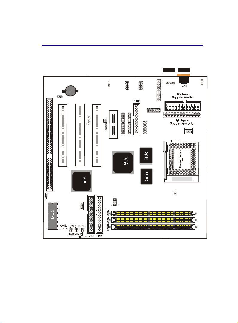
Uses 168-Pin DIMM modules x3 auto banking in multiple con-
figuration up to 640MB.
Support SDRAM/EDO DRAM Mode DRAM use 3.3 Votage 168-
pin DIMMx3.
Support Onboard Burst/Pipelined burst synchronous L2 Write
Back cache. The Cache memory combination could be 512K/1M.
3 PCI Bus slots, and 1 x 16 bits ISA Bus slots.
All 3 PCI slots support Master mode.
System BIOS support 4 IDE harddisk drivers that don't need de-
vice driver for S/W application, the capacity of each harddisk can
large than 528MB up to 8.4GB(or more).
PCI Bus master IDE interface on board with two connectors support
4 IDE devices in 2 channel, the PCI IDE Controller supports PIO
Mode 0 to Mode 4, Bus master IDE DMA Mode 2 and Ultra DMA
66MB
Support PS/2™ mouse Connector.
Support the Universal Serial Bus (U.S.B)

6 / Chapter 2 Features
System BIOS supports LS-120, ZIP driver firmware and
Green feature function, Plug and Play Flash ROM.
Use switching power supply to support CPU core voltage.
Support Software Virus Warning in BIOS
Support ACPI functionStatic Electricity Precautions

Chapter 3 Installation / 7
The 5VIA73 Mainboard layout
ISA SLOT1
JFAN1
PS/2
JIR1
JFAN2
Socket 7
K/B
CN2
CN3
LPT1
J3
JBAT1
1
J5
J6 J7
VGA
JWOL1
JP2
JP1
PS2
1
JTAG1
1
J2
1
11
USB2
12
USB1
12
2
2
COM1 COM2
12

8 / Chapter 2 Features
Installation
3
Chapter 3
Jumper
Jumper Refer to page
JBAT1 - Real time Clock RTC clean 12
JTAG1 - TAG RAM Voltage select 12
J2 - CD Line in 12
J8 - BIOS Voltage Select 13
J5, J6, J7 - AMR Control 13
JFAN1 - FAN CONN. for CPU 27
JFAN2 - FAN CONN. for System 27
JWOL1 - LAN Card Wake Up 31

Chapter 3 Installation / 9
Expansion Slot
Which to pages
168 pin DIMM Socket 16
Socket 370 17
PCI SLOT 1,2,3 -32bits PCI SLOT 25
ISA SLOT1 - 16bits ISA SLOT 25
Connectors Refer to page
USB1 - USB Port 25
USB2 - USB Port 25
COM1 - COM 1 serial port 25
COM2 - COM 2 serial port 25
LPT1 - Parallel port 25
FDC1 - FLOPPY connector 25
PS2 - PS/2 Mouse port. 26
CN2 - AT Keyboard port 26
IDE1 - Primary IDE connector 28
IDE2 - Secondary IDE connector 28
JIR1 - IrDA connector 28
PANAL 1 - HDD LED 29
PANAL 1 - Reset Switch 29
PANAL 1 - Speaker Connector 29
PANAL 1 - Power LED 29
PANAL 1 - ATX Power switch 29
CN2 - ATX Power Connector 30
CN3 - AT Power Connector 30
J3 - Audio & Game Port Connector 31

10 / Chapter 3 Installation
System Installation Setup
Before using your computer, you must finish the following steps:
1. Set jumpers on mainboard
2. Install SDRAM module.
3. Install the Processor.
4. Connect Ribbon Cables, Cabinet Wires, and Power supply.
5. Install Add on Cards.
6. Setup the BIOS software.
Static Electricity Precaution
Keep the mainboard and other system components in their anti-
static packaging until you are ready to install them.
Do all preparative work on a static-free surface with the main
board components facing up.
Unplug your computer when working on the inside.
Wear an Anti-static wrist strap.
Hold the system components, boards or cards by its edges only.
Be careful not to touch any of IC chips, circuitry, contacts or
connections, especially gold contacts on the mainboard.

Chapter 3 Installation / 11
Jumper Settings
Jumpers
Several hardware setting are made through the use of jumper caps to
connect jumper pins (Jxx) on the mainboard. See " Map of the
mainboard" for the locationed the jumpers.
The jumper settings will be described numerically such as [----], [1-2],
[2-3] for no connection, connect pins 1 & 2, and connect pins 2 & 3
respectively. Pin 1 for our mainboard is always on top one or on the
left when holding the mainboard with the keyboard away from
yourself. "P1" is written besides pin 1 on jumper with three pins. The
jumpers will also be shown graphically such as to connect pin
1&2 and to connect 2&3. Jumpers with two pins will be shown
as for Short (on )and for Open (off).For manufacturing
simplicity it may be sharing pins from other groups. Use the diagrams
in this manual instead of following the pin layout on the board. Set-
tings with two jumper numbers require that both jumpers be moved
together. To connect the pin, simply place a plastic jumper cap over
the two pins as diagrammed.

12 / Chapter 3 Installation
Real Time Clock (RTC) RAM - JBAT1 :
The CMOS RAM is powered by the onboard button cell battery. To
clear the RTC data:
(1)Turn off your computer, (2) Move this jumper to "2-3Pin Clear
Data", (3) Move the jumper back to "Default", (4) Turn on your
computer, (5) Hold down <Delete > during bootup and enter BIOS
setup to re-enter user Preferences. JBAT1 CMOS Clear
1-2 (default) Normal
2-3 Clear CMOS
P2 P3P1
P2 P3P1
TAG RAM Voltage Select - JTAG1 :
The 4-pin connectors enable the system to receive the audio output
from the CD-ROM.
CD LINE IN - J2 :
JTAG1
1-2 3.3V
2-3 5 V
(default)
P2
P3
P1
P2
P3
P1
J2
ISA SLOT1
JFAN1
PS/2
JIR1
JFAN2
Socket 7
K/B
PS2
CN2
CN3
LPT1
J3
COM1 COM2
USB2USB1
JBAT1
1
J5
J6 J7
JTAG1
VGA
JWOL1
J2
JP2
JP1
1

Chapter 3 Installation / 13
ISA SLOT1
JFAN1
PS/2
JIR1
JFAN2
Socket 7
K/B
PS2
CN2
CN3
LPT1
J3
COM1 COM2
USB2USB1
JBAT1
1
J5
J6 J7
JTAG1
VGA
JWOL1
J2
JP2
JP1
1
BIOS Voltage Select - J8 :
This allows you to select BIOS Voltage setting function.
AMR Contorl - J5, J6, J 7 :
P2
P3
P1
P2
P3
P1
J8
1-2 5 V
(Default)
2-3 12V
This mainboard provides a AMR slot. You may be enabled or disa-
bled according as your sound card's functions:
J5 J6 J7 Description
CLOSE CLOSE 1-2 AC'97 Function
CLOSE OPEN 3-4 MC'97 Function
CLOSE CLOSE 1-2,3-4 AC'97 +MC'97 Function
CLOSE OPEN 3-4 AMR Function
Note :
You must configure the setting for "Onboard Sound : Disa-
bled" in Chipset Feature Setup and "Onboard Legacy Au-
dio : Disabled" in Integrated Peripherals.
Please insert a sound card to PCI1 slot

14 / Chapter 3 Installation
System Memory ( DIMM Module)
This 5VIA73 main board supports three 168 pins DIMM of 16 MB,
32 MB, 64 MB, 128 MB ,256MB to form a memory size between 16MB
to 256MB.
The DRAM can be either 45ns,50ns,or 60ns 3.3v SDRAM,and 3.3v
Enhanced Data Output (EDO) RAM.
Install memory in any or all Banks in Combination:
Bank Memory module
DIMM 1 16MB,32MB,64MB,128MB,128MB
( Bank 0-1 ) 168 pin,3.3v SDRAM / EDO RAM
DIMM 2 16MB,32MB,64MB,128MB,256MB
( Bank 2-3 ) 168 pin 3.3v,SDRAM / EDO RAM
DIMM 3 16MB,32MB,64MB,128MB,256MB
( Bank 4-5 ) 168 pin 3.3v,SDRAM / EDO RAM
Total System Memory(Max 640 MB)
Note :
The DIMM Slot does not support any 5v EDO DIMM
module.
The DIMM Slot does not support any 5v SDRAM DIMM
module.
Memory speed setup is required through "Auto Con-
figuration" in BIOS chipset Setup of BIOS
SOFTWARE. If several speed memorious are used, You
must set Auto Configuration to low. Example If both
50ns, 60ns are used, Please set Auto configuration to
60ns.
It's allowed any DIMM module put in any DIMM slot.
It's allowed there are different capacity DIMM module
in all DIMM slot.

Chapter 3 Installation / 15
DIMM Memory Installation
Insert the module (s) as shown. Because the number pins are differ-
ent on either side of the breaks,the module will only fit in the orienta-
tion as shown. SDRAM DIMM modules have different pin contacts
on each side and therefore have a higher pin density.
168 Pin DIMM Socket
88 pins 60 pins 20 pins
ISA SLOT1
JFAN1
PS/2
JIR1
JFAN2
Socket 7
K/B
PS2
CN2
CN3
LPT1
J3
COM1 COM2
USB2USB1
JBAT1
1
J5
J6 J7
JTAG1
VGA
JWOL1
J2
JP2
JP1
1

16 / Chapter 3 Installation
The Dual Inline Memory Module (DIMM) memory module must
be 3.3v Extended Data Output (EDO) DRAM or SDRAM. You can
identify the type of DIMM module by the illustration below:
168 Pin DRAM DIMM Notch Key Definitions
The notch on the DIMM module will shift between left, center, or
right to identify the type and also to prevent the wrong type to be
inserted into the DIMM slot on the Mainboard. You must ask your
retailer for Specifications before purchasing.
Four clock signals are supported on this mainboard
RFU Unbuffered
Buffered
5.0V Reserved
3.3V
DRAM Key Position Voltage Key Position

Chapter 3 Installation / 17
CPU Installation
The motherboard provides a ZIF socket 7. The CPU that came with
the motherboard should have a fan attached to it to prevent over-
heating . If this is not the case then purchase a fan before you turn on
your system.
To install a CPU , first turn off your system and remove its cover.
Locate the ZIF socket and open it by first pulling the lever sideways
away from the socket then upwards to a 90-degree right angle. Insert
the CPU with the correct orientation shown . The notched corner
should point towards the end of the lever. Because the CPU has a
corner pin for two of the four corners, the CPU will only fit in the
orientation as shown.
Socket 7
Notch
JP1 CPU Core Voltage Selection (1-5)

18 / Chapter 3 Installation
JP1 CPU Core Voltage Selection (1-5)
Refer to the following table for more CPU core Voltage selection jumper
setting:
CPU Voltage 9-10 7-8 5-6 3-4 1-2 Vcore
OFF OFF OFF OFF OFF 0
OFF OFF OFF OFF ON 2.1
OFF OFF OFF ON OFF 2.2
OFF OFF OFF ON ON 2.3
OFF OFF ON OFF OFF 2.4
OFF OFF ON OFF ON 2.5
OFF OFF ON ON OFF 2.6
OFF OFF ON ON ON 2.7
OFF ON OFF OFF OFF 2.8
OFF ON OFF OFF ON 2.9
OFF ON OFF ON OFF 3.0
OFF ON OFF ON ON 3.1
OFF ON ON OFF OFF 3.2
OFF ON ON OFF ON 3.3
OFF ON ON ON OFF 3.4
OFF ON ON ON ON 3.5

Chapter 3 Installation / 19
JP1 CPU Core Voltage Selection (1-5)
Refer to the following table for more CPU core Voltage selection jumper
setting:
CPU Voltage 9-10 7-8 5-6 3-4 1-2 Vcore
ON ON ON ON ON 2.05
ON ON ON ON OFF 2.00
ON ON ON OFF ON 1.95
ON ON ON OFF OFF 1.90
ON ON OFF ON ON 1.85
ON ON OFF ON OFF 1.8
ON ON OFF OFF ON 1.75
ON ON OFF OFF OFF 1.7
ON OFF ON ON ON 1.65
ON OFF ON ON OFF 1.6
ON OFF ON OFF ON 1.55
ON OFF ON OFF OFF 1.50
ON OFF OFF ON ON 1.45
ON OFF OFF ON OFF 1.40
ON OFF OFF OFF ON 1.35
ON OFF OFF OFF OFF 1.30

20 / Chapter 3 Installation
JP1 CPU Ratio Selection (6-8)
This Jumpter set the frequency ratio between the internal frequency
of the CPU and the external frequency (called the bus clock) within
the CPU. These must be set together with the above Jumpter
CPU model ratio bus frequency.
JP1 CPU Ratio Selection (6-8)
CPU Ratio 15-16 13-14 11-12 Ratio
OFF ON ON 2.5
OFF ON OFF 3.0
OFF OFF ON 2.0
OFF OFF OFF 1.5/3.5
ON ON ON 4.5
ON ON OFF 5.0
ON OFF ON 4.0
ON OFF OFF 5.5
Table of contents
Other Acorp Motherboard manuals