Acorp 694XT User manual

The information presented in this publication has been
carefully prepared to ensure reliability ; however, no
responsibility is assumed for inaccuracies.
Specifications are subject to change without notice.
IBM, PC/AT, and PC/XT are trademarks of Interna-
tional Business Machines Corporation.
Pentium is a trademark of Intel Corporation
AWARD is a registered trademark of Phoenix
Software Inc.
MS-DOS and WINDOWS NT are registered trade-
marks of Microsoft Corporation.
Trademarks and/or registered trademarks are the
properties of their respective owners.
User's Manual Version 1.1
694XT
i

Table of Contents
IntrnctctinnIntrnctctinn
Intrnctctinn
1. Mnthdranarc Ddrcriotinn1. Mnthdranarc Ddrcriotinn
1. Mnthdranarc Ddrcriotinn
1.1 Fdattrdr
1.1.1 Harcward 2
1.1.2 Snetward 4
1.1.3 Attachmdntr4
1.2 Mnthdranarc Inrtallatinn
1.2.1 Layntt ne Mnthdranarc 5
1.3 Mnthdranarc Cnnndctnrr
1.3.1 Frnnt Pandl Cnnndctnrr(PANEL1(7
1.3.2 Flnooy Dirk Cnnndctnr(FDD1(8
1.3.3 Harc Dirk Cnnndctnrr(IDE1.IDE2(8
1.3.4 ATW 2/-oin Pnwdr Cnnndctnr(PW1.PW2(9
1.3.5 Inerardc Cnnndctnr(IR(9
1.4 Back Pandl Cnnndctnrr
1.4.1 MS1 Mntrd.Kdyanarc CNNN. 1/
1.4.2 USB Cnnndctnrr(USB1.USB2(1/
1.5 Sdrial anc Paralldl Intdreacd onrtr11
1.6 CPU Inrtallatinn
1.6.1 CPU Inrtallatinn Prnctct(Snckdt 37/(13
1.6.2 CPU Clnck Sdtting(JCK1~JCK4,JC1,JC3(14
1.7 Jtmodr Sdtting
1.7.1 CPU Fan Cnnndctnrr(FAN1.2(15
1.7.2 Wakd-Nn-Lan Hdacdr(WNL1(16
1.7.3 AMR Ftnctinn Sdldctinn(J1(16
1.7.4 CMNS Ftnctinn Sdldctinn(JBAT1(16
1.7.5 CPU Tyod Sdldctinn(JC1~JC2,JC4~JC5(17
ii

Table of Contents
1.8 DRAM Inrtallatinn
1.8.1 DIMM 18
1.8.2 Hnw tninrtall aDIMM Mnctld 18
1.9 AtcinStaryrtdm
1.9.1 CD-Atcin-IN Cnnndctnrr(CDIN1.CDIN2(19
1.9.2 Atcin& Cnnndctnrr(Atcin( 19
2. BINS Sdtto2. BINS Sdtto
2. BINS Sdtto
2.1 Main Mdnt23
2.2 Stancarc CMNS Fdattrdr26
2.3 Acuancdc BINS Fdattrdr29
2.4 Acuancdc Chiordt Fdattrdr33
2.5 Intdgratdc Pdriohdralr38
2.6 Pnwdr Managdmdnt Sdtto43
2.7 PnP.PCI Cnneigtratinnr49
2.8 PC Hdalth Stattr 53
2.9 Frdqtdncy.Vnltagd Cnntrnl54
2.1/ Lnac Fail-Saed Ddeatltr56
2.11 Lnac Notimizdc Ddeatltr57
2.12 Sdt Stodruirnr.trdr Parrwnrc 58
2.13 Saud & Exit Sdtto6/
2.14 Exit Withntt Sauing 61
iii

Chapter 1 Motherboard Description / 1
Introduction
System Overview
This manual was written to help you start using this product
as quickly and smoothly as possbile. Inside, you will find
the answers to solve most problems. In order for this
reference material to be of greatest use, refer to the
“expanded table of contents” to find relevant topics.
This board provides a total PC solution by incorporating the
System , I/O , and PCI IDE. The mainboard is designed for
Intel PIII/Celeron/Coppermine processors base PC ATX
system, support single processors with ISA Bus, AMR Bus,
PCI Local Bus, and AGP Bus to support upgrades to your
system performance. It is ideal for multi-tasking and fully
supports MS-DOS, Windows, Windows NT , Windows ME,
Windows 2000 , Novell, OS/2, Windows95/98 , UNIX ,
Windows98SE, SCO UNIX etc.
This manual also explains how to install the mainboard for
operation, and how to setup your CMOS configuration with
the BIOS setup program.

2 / Chapter 1 Motherboard Description
1.Motherboard Description
1.1 Features
1.1.1 Hardware
CPU
-Socket 370 for Intel PPGA/FC-PGA PII/PIII processor.
-Intel FC-PGA/PPGA Celeron Processors
300MHz~600MHz or higher processor with 66MHz FSB.
-Intel FC-PGA Pentium III Processors 500MHz~933MHz
or higher processor with 100/133MHz FSB.
-VIA Cyrix III Processors.
Chipset
-North Bridge System Chipset : VT82C694X
-Sourth Bridge System Chipset: VT82C686A
Biggest memory capacity
694XT is equipped with three DIMM socket to support
(16MB, 32MB, 64MB, 128MB, 256MB) 168 pin 3.3v
SDRAM SPD(Special Presence Detect).Maximum
memory up to 768MB.
AGP for fast VGA solution
-AGP specification compliant.
-AGP 66 MHz 3.3v/1.5v for 2X/4X device support.
Note:
If an unstable issue occurs, after installing " VIA 4 in 1 driver
". We suggest you to re-install " VIA 4 in 1 driver ", and then
select " install VIA AGP VxD in Standard mode " at
" VIA_GART AGP Driver " item.
PCI Expansion Slot
Provide one 16 bit ISA, and three 32 bit PCI slots .
On-Board IDE
-An IDE controller on the VIA VT82C686A Chipset pro-
vides IDE HDD/CD-ROM with PIO,Bus Master and Ultra
DMA 33/66 operation modes.
-Can connect up to four IDE devices.

Chapter 1 Motherboard Description / 3
On-Board Peripherals:
-1 floppy port supports 2 FDD with 360K,720K,1.2M,
1.44M and 2.88M byte.
-2 serial ports (COM1+COM2).
-1 parallel port supports SPP/EPP/ECP mode.
-1 IrDA/HP connector for SIR.
Audio
-AC’97 CODEC on board, support 3D sound.
BIOS
- The mainboard BIOS provides “Plug & Play” BIOS which
detects the peripheral devices and expansion cards of the
board automatically.
- The mainboard provides a Desktop Management Interface
(DMI) function which records your mainboard
specifications.
- BIOS support CD-ROM, SCSI, LAN BOOT, Temperature
sensor, Wake on modem, LAN, Alarm Bus CLK setup with
BIOS.
WOL (Wake On LAN)
Supports system power up from LAN ring up .
IrDA Port
Support this serial fast communication up to 115.2Kbps.
Support Ring on by modem/Alarm on (ATX only)
Support System power up from Modem ring up or timer
of System. Required enabled in Ring on by modem and
Alarm on in BIOS.
Supports ACPI function for ATX Power.
Support AT/ATX Power supply(20pin) connector.

4 / Chapter 1 Motherboard Description
1.1.2 Software
BIOS
-AWARD legal BIOS.
-Supports APM 1.2.
-Supports USB Function.
-Supports ACPI
Operation System
-Offers the highest performance for MS-DOS, Windows,
Windows NT, Windows ME, Windows 2000, Novell, OS/2,
Windows95/98, Windows98SE, UNIX, SCO UNIX etc.
1.1.3 Attachments
-HDD UDMA66 Cable.
-FDD Cable.
-Flash Memory Written for BIOS Update.
-USB Cable. (option)
-Audio Cable.
-PS2/Print Port Cable.
-COM1/COM2 Cable.
-Fully Setup CD Driver built in Utility(Ghost, Anitivirus,
Adobe Acrobat...).
-This manual.

Chapter 1 Motherboard Description / 5
1.2 Motherboard Installation
1.2.1 Layout of Motherboard
IR
K/B
PW1
ISA SLOT
WOL1
MS1
1
JBAT1
1
FAN1
FAN2
PCI1
PCI2
PCI3
JC1
JC3
JC4
JC5
1
1
1
1
COM2
11
COM1
11
USB1
11
LPT
AMR
AGP SLOT
USB2
11
1
ISA SOLT
DIMM
PW2
Socket 370
SOCKET
AGP SOLT
IDE FDD
AMR SOLT
1
AUDIO
11
JCK4
JCK3
JCK2
JCK1

6 / Chapter 1 Motherboard Description
1.3 Motherboard Connectors
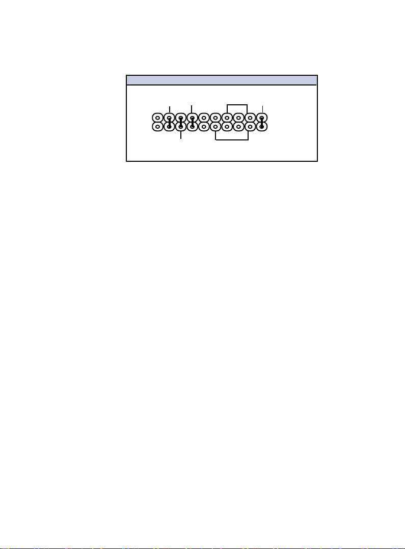
1.Back Oanek I.OBnnnecsnrr1.Back Oanek I.OBnnnecsnrr
1.Back Oanek I.OBnnnecsnrr1.BCAtcin-In Bnnnecsnr1.BCAtcin-In Bnnnecsnr
1.BCAtcin-In Bnnnecsnr1.BCAtcin-In Bnnnecsnr
1.BCAtcin-In Bnnnecsnr
3.AMR BOCDB Etncsinn(J1(3.AMR BOCDB Etncsinn(J1(
3.AMR BOCDB Etncsinn(J1(4.Wake-On-LANBnnnecsnr4.Wake-On-LANBnnnecsnr
4.Wake-On-LANBnnnecsnr4.Wake-On-LANBnnnecsnr
4.Wake-On-LANBnnnecsnr
5.Ernns Twn BOM Bnnnecsnrr5.Ernns Twn BOM Bnnnecsnrr
5.Ernns Twn BOM Bnnnecsnrr6.Ernns Oanek Bnnnecsnr6.Ernns Oanek Bnnnecsnr
6.Ernns Oanek Bnnnecsnr6.Ernns Oanek Bnnnecsnr
6.Ernns Oanek Bnnnecsnr
7.Ean Bnnnecsnrr(Ean1.1(7.Ean Bnnnecsnrr(Ean1.1(
7.Ean Bnnnecsnrr(Ean1.1( 8.ICD Bnnnecsnrr8.ICD Bnnnecsnrr
8.ICD Bnnnecsnrr8.ICD Bnnnecsnrr
8.ICD Bnnnecsnrr
9.Atcin Bnnnecsnr9.Atcin Bnnnecsnr
9.Atcin Bnnnecsnr10.Eknooy Bnnnecsnr10.Eknooy Bnnnecsnr
10.Eknooy Bnnnecsnr10.Eknooy Bnnnecsnr
10.Eknooy Bnnnecsnr
11.IR Bnnnecsnr11.IR Bnnnecsnr
11.IR Bnnnecsnr
11.BOUBknck Sekecsinn(JBJ1~JBJ4,JB1,JB3(11.BOUBknck Sekecsinn(JBJ1~JBJ4,JB1,JB3(
11.BOUBknck Sekecsinn(JBJ1~JBJ4,JB1,JB3(
13.AT.ATXOnwer Bnnnecsnr13.AT.ATXOnwer Bnnnecsnr
13.AT.ATXOnwer Bnnnecsnr
14.BOUTyoe Sekecs(JB1~JB1,JB4~JB5(14.BOUTyoe Sekecs(JB1~JB1,JB4~JB5(
14.BOUTyoe Sekecs(JB1~JB1,JB4~JB5(
15.BMOS EtncsinnSekecsinn(JBAT1(15.BMOS EtncsinnSekecsinn(JBAT1(
15.BMOS EtncsinnSekecsinn(JBAT1(
IR
K/B
PW1
ISA SLOT
MS1
1
JBAT1
1
FAN1
FAN2
PCI1
PCI2
PCI3
JC1
JC3
JC4
JC5
1
1
1
1
COM2
11
COM1
11
USB1
11
LPT
AMR
AGP SLOT
USB2
11
1
ISA SOLT
DIMM
PW2
Socket 370
SOCKET
AGP SOLT
IDE FDD
AMR SOLT
1
AUDIO
11
WOL1
JCK4
JCK3
JCK2
JCK1
1
13
10
11
1
5
1
9
4
2
7
8
6
15
12
3
14

Chapter 1 Motherboard Description / 7
1.3.1 Front Panel Connector(PANEL1)
PANEL1 Connector
Speaker Connector (SPK)
An offboard speaker can be installed onto the motherboard as a
manufacturing option. An offboard speaker can be connected to
the motherboard at the front pannel connector. The speaker
(onboard or offboard) provides error beep code information dur-
ing the Power Self-Test when the computer cannot use the video
interface. The speaker is not connected to the audio subsystem
and does not receive output from the audio subsystem.
Hard Drive LED Connector (HDD)
This connector supplies power to the cabinet IDE activity LED.
Read and write activity by devices connected to the Primary or
Secondary IDE connectors will cause the LED to light up.
SMI Suspend Switch Lead (SMI)
This allows the user to manually place the system into a suspend
mode of Green mode. System activity will be instantly decreased
to save electricity and expand the life of certain components
when the system is not in use. This 2-pin connector (see the
figure below) connects to the case-mounted suspend switch. If
you do not have a switch for the connector, you may use the
"Turbo Switch” instead since it does not have a function. SMI is
activated when it detects a short. It may require one or two
pushes depending on the position of the switch. Wake-up can be
controlled by settings in the BIOS but the keyboard will always
allow wake-up (the SMI Suspend Switch Lead cannot wake-up
the system). If you want to use this connector, the "Suspend
Switch" in the Power Management Setup of the BIOS SOFT-
WARE section should be on the default setting of Enable.
SPK
PW_BN
1
2
RST HDD PW_LED
+
++
+
SMI

8 / Chapter 1 Motherboard Description
ATX Power Switch (PW_BN)
The system power is controlled by a momentary switch
connected to this lead. Pushing the button once will switch
the system ON. The system power LED lights when the
system's power is on .
Power LED Lead (PW_LED)
The system power LED lights when the system power is on.
Reset Switch Lead (RST)
The connector can be connected to a momentary SPST type
switch that is normally open. When the switch is closed,the
motherboard resets and runs the POST.
1.3.2 Floppy Disk Connector(FDD1)
This connector supports the provided floppy drive ribbon
cable. After connecting the single end to the board, connect
the two plugs on the other end to the floppy drives.
1.3.3 Hard Disk Connectors(IDE1/IDE2)
These connectors support the provided IDE hard disk ribbon
cable. After connecting the single end to the board, connect
the two plugs at the other end to your hard disk.
If you install two hard disks, you must configure the second
drive to Slave mode by setting its jumper settings. BIOS now
supports SCSI device or IDE CD-ROM boot up (see "HDD
Sequence SCSI/IDE First" & "Boot Sequence" in the BIOS
Features Setup of the BIOS SOFTWARE) (Pin 20 is removed
to prevent inserting in the wrong orientation when using
ribbon cables with pin 20 plugged) .

Chapter 1 Motherboard Description / 9
1.3.4 ATX/AT Power Supply Connector (20-pin block)
- PW1/PW2
This connector supports the power button on-board. Using
the ATX power supply, functions such as Modem Ring Wake-
Up and Soft Power Off are supported on this motherboard .
This power connector supports instant power-on
functionality, which means that the system will boot up
instantly when the power connector is inserted on the board.
1.3.5 Infrared Connector(IR)
After the IrDA interface is configured, files can be
transferred from or to portable devices such as laptops,
PDAs, and printers using application software.
Pin Signal Pin Signal
1 3.3V 11 3.3V
2 3.3V 12 -12V
3 GND 13 GND
4 5V 14 PS-ON
5 GND 15 GND
6 5V 16 GND
7 GND 17 GND
8 PW-OK 18 -5V
9 5V_SB 19 5V
10 12V 20 5V

10 / Chapter 1 Motherboard Description
IR
K/B
PW1
ISA SLOT
MS1
1
JBAT1
1
FAN1
FAN2
PCI1
PCI2
PCI3
JC1
JC3
JC4
JC5
1
1
1
1
COM2
11
COM1
11
USB1
11
LPT
AMR
AGP SLOT
USB2
11
1
ISA SOLT
DIMM
PW2
Socket 370
SOCKET
AGP SOLT
IDE FDD
AMR SOLT
1
AUDIO
11
JCK4
JCK3
JCK2
JCK1
WOL1
1.4 Back Panel Connectors
1.4.1 Keyboard CONN.
This connector will compatible with standard at AT size (large
DIN) keyboard plugs. You may use a DIN to mini DIN adapter
on standard AT keyboards.
Mouse Port
This system will direct IRQ12 to PS/2 mouse.
1.4.2 USB Connectors:USB1/USB2
The motherboard provides a OHCI(Open Host Controller
Interface)Universal Serial Bus Roots for attaching USB
devices such as a keyboard, mouse and other USB devices.
You can plug the USB devices directly into this connector.
Four USB ports are available on the back panel.Therefore,
we have a solution to provide a 10 pin ribbon cable with
bracket to connect Built-in on-board USB header by optional.
1
3
5
7
9
VCC
P0-
P0+
GND
GND
2
4
6
8
10
GND
GND
P1+
P1-
VCC

Chapter 1 Motherboard Description / 11
1.5 Serial and Parallel Interface Ports
This system comes equipped with two serial ports and one
parallel port. Both types of interface ports will be explained
in this chapter.
The Serial Interfaces:COM1/COM2
The serial interface port is sometimes refered to as an RS-
232 port or an asynchronous communication port. Mice,
printers, modems and other peripheral devices can be
connected to a serial port. The serial port can also be used
to connect your computer system. If you wish to transfer
the contents of your hard disk to another system it can be
accomplished by using each machine’s serial port.
1
COM1/COM2
IR
K/B
PW1
ISA SLOT
MS1
1
JBAT1
1
FAN1
FAN2
PCI1
PCI2
PCI3
JC1
JC3
JC4
JC5
1
1
1
1
COM2
11
COM1
11
USB1
11
LPT
AMR
AGP SLOT
USB2
11
1
ISA SOLT
DIMM
PW2
Socket 370
SOCKET
AGP SOLT
IDE FDD
AMR SOLT
1
AUDIO
11
WOL1
JCK4
JCK3
JCK2
JCK1

12 / Chapter 1 Motherboard Description
Parallel Interface Port
Unlike serial ports, parallel interface ports have been
standardized and should not present any difficulty interfacing
peripherals to your system. Sometimes called a Centronics port,
the parallel port is almost exclusively used with printers.
LPT
IR
K/B
PW1
ISA SLOT
MS1
1
JBAT1
1
FAN1
FAN2
PCI1
PCI2
PCI3
JC1
JC3
JC4
JC5
1
1
1
1
COM2
11
COM1
11
USB1
11
LPT
AMR
AGP SLOT
USB2
11
1
ISA SOLT
DIMM
PW2
Socket 370
SOCKET
AGP SOLT
IDE FDD
AMR SOLT
1
AUDIO
11
JCK4
JCK3
JCK2
JCK1
WOL1

Chapter 1 Motherboard Description / 13
1.6 CPU Installation
1.6.1 CPU Installation Procedure:Socket 370
1. Pull the lever sideways away from the socket then raise
the lever to a 90-degree angle.
2. Locate Pin 1 in the socket and look for the white dot or
cut edge in the CPU. Match Pin 1 with the white dot/cut
edge then insert the CPU.
3. Press the lever down to complete the installation.
4.Make sure the spec of the heatsink is good enough.
Notch
IR
K/B
PW1
ISA SLOT
MS1
1
JBAT1
1
FAN1
FAN2
PCI1
PCI2
PCI3
JC1
JC3
JC4
JC5
1
1
1
1
COM2
11
COM1
11
USB1
11
LPT
AMR
AGP SLOT
USB2
11
1
ISA SOLT
DIMM
PW2
Socket 370
SOCKET
AGP SOLT
IDE FDD
AMR SOLT
1
AUDIO
11
JCK4
JCK3
JCK2
JCK1
WOL1

14 / Chapter 1 Motherboard Description
1.6.2 CPU Clock Selection: JCK1~JCK4, JC1, JC3
The JCK1~4 jumpers are used to set the PCI and CPU external bus
clock.
FEQ. JCK1 JCK2 JCK3 JCK4 JC1 JC3
66MHz 1-2 1-2 2-3 2-3 OPEN OPEN
100MHz 1-2 1-2 1-2 2-3 OPEN OPEN
133MHz 1-2 1-2 1-2 1-2 OPEN OPEN
Auto 1-2 1-2 OPEN OPEN 2-3 CLOSE
(Intel)
Auto 1-2 1-2 OPEN OPEN 1-2 CLOSE
(VIA-Cyrix)
Close: (SHORT)
Open:
IR
K/B
PW1
ISA SLOT
MS1
1
JBAT1
1
FAN1
FAN2
PCI1
PCI2
PCI3
JC1
JC3
JC4
JC5
1
1
1
1
COM2
11
COM1
11
USB1
11
LPT
AMR
AGP SLOT
USB2
11
1
ISA SOLT
DIMM
PW2
Socket 370
SOCKET
AGP SOLT
IDE
FDD
AMR SOLT
1
AUDIO
11
WOL1
JCK4
JCK3
JCK2
JCK1

Chapter 1 Motherboard Description / 15
1.7 Jumper Setting
A jumper has two or more pins that can be covered by a
plastic jumper cap, allowing you to select different system
options.
1.7.1 CPU/System Fan Connector:Fan1/2
Pin Assignment
1 Ground
2 +12VDC
3 Signal
FAN 2
Connector
1
3
2
J1
WOL1
Connector
JBAT1
FAN 1
Connector
JC2JC1
JC3
JC4
JC5
IR
K/B
PW1
ISA SLOT
MS1
1
JBAT1
1
FAN1
FAN2
PCI1
PCI2
PCI3
JC1
JC3
JC4
JC5
1
1
1
1
COM2
11
COM1
11
USB1
11
LPT
AMR
AGP SLOT
USB2
11
1
ISA SOLT
DIMM
PW2
Socket 370
SOCKET
AGP SOLT
IDE FDD
AMR SOLT
1
AUDIO
11
JCK4
JCK3
JCK2
JCK1
WOL1

16 / Chapter 1 Motherboard Description
1.7.3 AMR Set Function: J1
Pin Assignment
Enabled AMR Slot
(Default)
Disabled AMR Slot
1.7.4 CMOS Function Selection: JBAT1
Pin Assignment
1-2 Normal (Default)
2-3 Clear CMOS
NOTE:
(Please follow the procedure below to clear CMOS data.)
(1)Remove the AC power line.(2)JBAT1(2-3)Closed.(3)Wait five
seconds.(4)JBAT1(1-2) Closed.(5)AC Power on.(6)Reset your
desired password or clear CMOS data.
1.7.2 Wake-On LAN Header: WOL1
Pin Assignment
1 5VSB
2 Ground
3 Signal
3
1

Chapter 1 Motherboard Description / 17
1.7.5 CPU Type Select: JC1~JC2, JC4~JC5
Current PCI bus in limited to 33MHz, socket370 Celeron
processors limited to 66MHz, and SDRAM limited to the
DIMM type 66/100/133MHz. Other settings are for
experienced users only.
IR
K/B
PW1
ISA SLOT
MS1
1
JBAT1
1
FAN1
FAN2
PCI1
PCI2
PCI3
JC1
JC3
JC4
JC5
1
1
1
1
COM2
11
COM1
11
USB1
11
LPT
AMR
AGP SLOT
USB2
11
1
ISA SOLT
DIMM
PW2
Socket 370
SOCKET
AGP SOLT
IDE FDD
AMR SOLT
1
AUDIO
11
WOL1
JCK4
JCK3
JCK2
JCK1
CPU Type JC1 JC2 JC4 JC5
Intel old
(PPGA)
Intel new
(FC-PGA)
VIA-Cyrix
JC4JC2 JC5JC1
JC4JC2 JC5JC1
JC4JC2 JC5JC1
Other Acorp Motherboard manuals