[AKD4953-A]
<KM101802> 2010/04
- 2 -
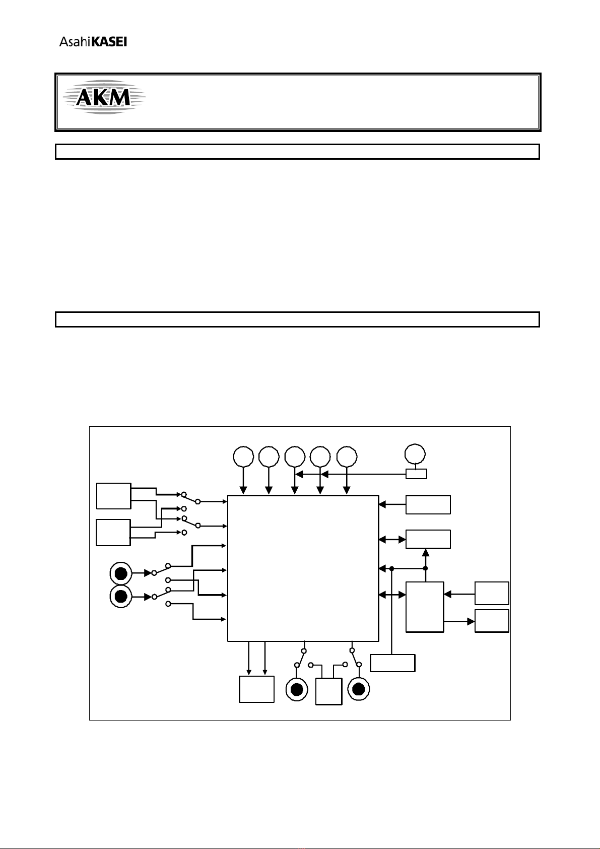
Operation Sequence
(1) Set up the power supply lines.
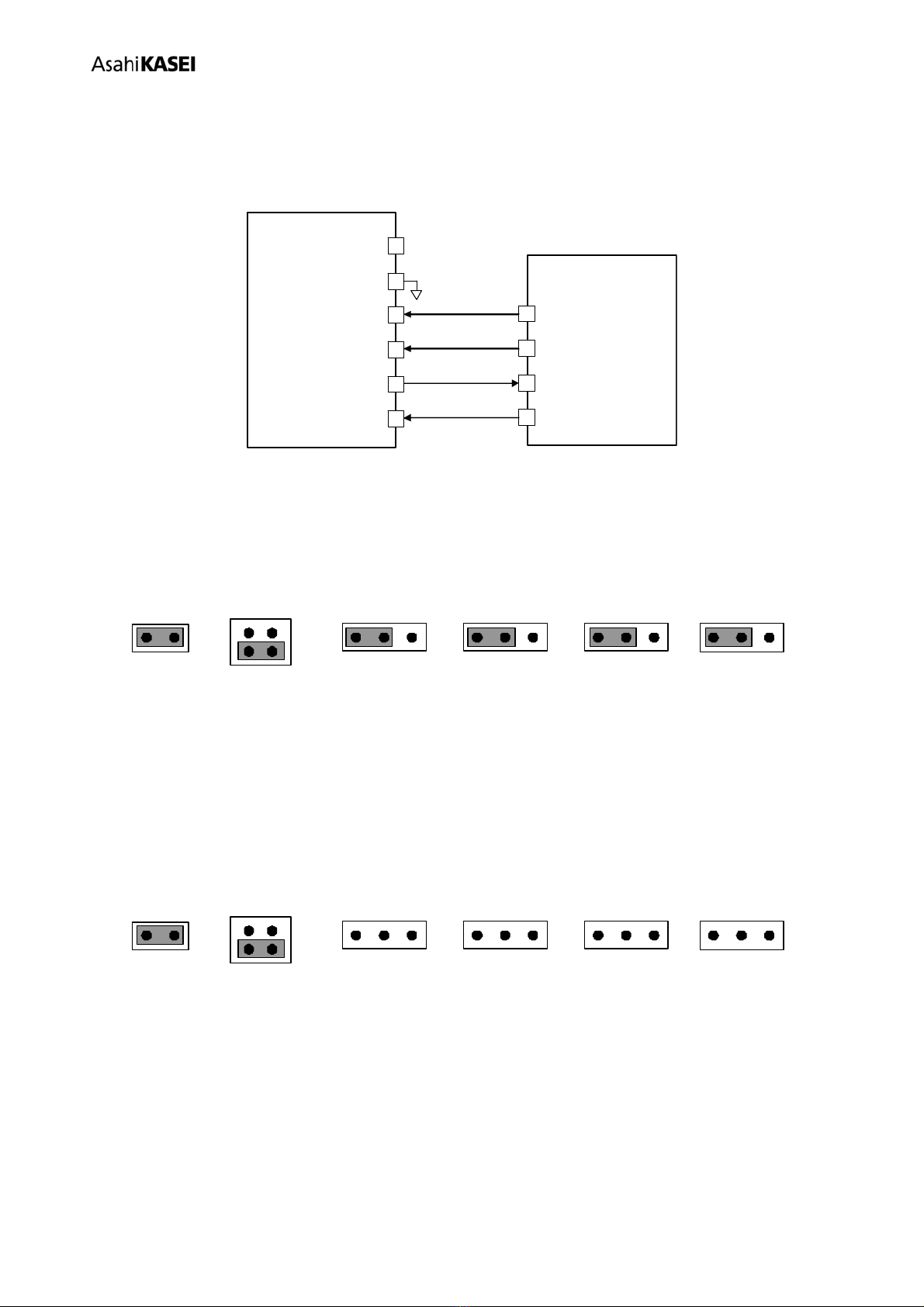
(1-1) In case of using the regulator. <Default>
JP3
SVDD-SEL JP4
AVDD-SEL JP6
TVDD-SEL JP7
VCC-SEL
Name of
Jack
Color Default Setting Using
REG red 5V for regulator (3.3V output : AVDD ,SVDD)
AVDD orange Open for AVDD of AK4953
SVDD orange Open for SVDD of AK4953
DVDD orange 1.6~2.0V (typ1.8V) for DVDD of AK4953
TVDD orange 1.6~3.5V (typ3.3V) for TVDD of AK4953
VCC orange Open for logic
D3V orange 2.7~3.6V (typ3.3V) for AK4118A and logic
AGND black 0V for analog ground
DGND black 0V for logic ground
Table 1. Set up of power supply lines
(1-2) In case of using the power supply connectors.
JP3
SVDD-SEL JP4
AVDD-SEL JP6
TVDD-SEL JP7
VCC-SEL
Name of
Jack
Color Default Setting Using
REG red Open No using
AVDD orange 3.0~3.5V (typ3.3V) for AVDD of AK4953
SVDD orange 0.9~5.5V (typ3.3V) for SVDD of AK4953
DVDD orange 1.6~2.0V (typ1.8V) for DVDD of AK4953
TVDD orange 1.6~3.5V (typ3.3V) for TVDD of AK4953
VCC orange 1.6~3.5V (typ3.3V) for logic(This voltage must be same as TVDD)
D3V orange 2.7~3.6V (typ3.3V) for AK4118A and logic
AGND black 0V for analog ground
DGND black 0V for logic ground
Table 2. Set up of power supply lines
* Each supply line should be distributed from the power supply unit.
(2) Set up the evaluation mode, jumper pins and DIP switch. (See the followings.)
(3) Power on.
The AK4953 and AK4114 should be reset once bringing SW1 (PDN) and SW2 (DIR) “L” upon power-up.
Click the reset button on the control software after releasing the reset by SW1= “H”.