[AKD4128A-A]
[KM104301] 2010/09
- 2 -
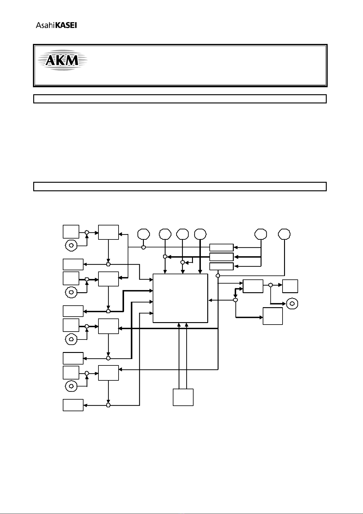
Operation sequence
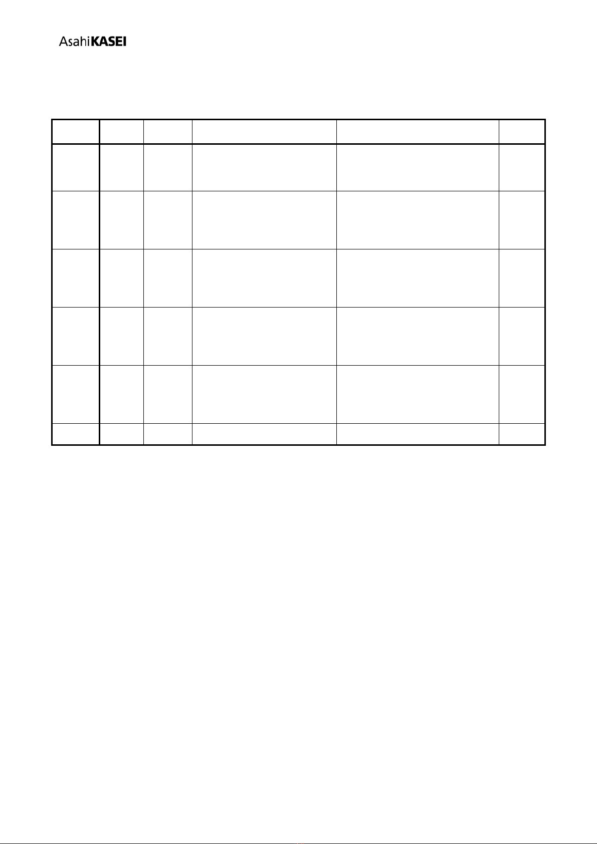
1) Set up the power supply lines.
Name of
jack Color
of jack Typ
Voltage Used for Open / Connect Default
Setting
+5V Orange +5V
Regulator T1,T2,T3:
AVDD and DVDD of
AK4128A, AK4114, Digital
Logic
Should be always connected
When default setting. +5V
AVDD Red +3.3V AVDD of AK4128A
Should be always connected
when AVDD of AK4128A is not
supplied from regulator T1.
In this case “JP1” is set to “AVDD”
side.
Open
DVDD Red +3.3V DVDD of AK4128A
Should be always connected
when DVDD of AK4128A is not
supplied from regulator T1.
In this case “JP2” is set to
“DVDD” side.
Open
D3.3V-1 Red +3.3V AK4114, Digital Logic
Should be always connected
when AK4114 and Digital Logic is
not supplied from regulator T2.
In this case “JP3” is set to
“D3.3V-1” side.
Open
D3.3V-2 Red +3.3V AK4114, Digital Logic
Should be always connected
when AK4114 and Digital Logic is
not supplied from regulator T3.
In this case “JP4” is set to
“D3.3V-2” side.
Open
GND Black 0V Ground Should be always connected GND
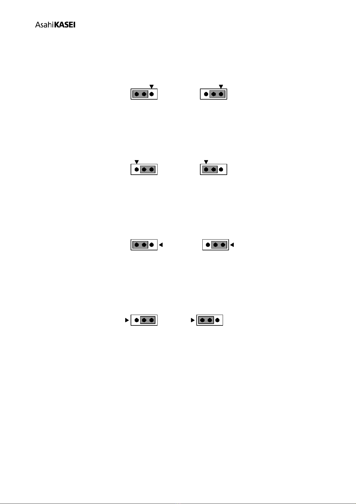
Table 1. Set up the power supply lines
Each supply line should be distributed from the power supply unit.