AKM AKD5366 User manual

[AKD5366]
<KM073601> 2007/04
- 1 -
GENERAL DESCRIPTION
AKD5366 is an evaluation board for the digital audio 24bit 48kHz A/D converter, AK5366. The AKD5366
includes the input circuit and also has a digital interface transmitter. Further, the AKD5366 can achieve
the interface with digital audio systems via opt-connector.
Ordering guide
AKD5366 --- AK5366 Evaluation Board
(Cable for connecting with printer port of IBM-AT,
compatible PC and control software are packed with this.)
FUNCTION
•DIT with optical output
•BNC connector for an external clock input
•10pin Header for serial control mode
LIN1-5
RIN1-5
AVDD,DVDD,TVDD
AK4103
(DIT) Opt
Out
Clock
Generator ROM Data
10pin Header
Control
Data
10pin Header
AVSS,DVSS
AK5366
Figure 1. AKD5366 Block Diagram
* Circuit diagram and PCB layout are attached at the end of this manual.
A
K5366 Evaluation Board Rev.
A
AKD5366

[AKD5366]
<KM073601> 2007/04
- 2 -
Evaluation Board Manual
Operation sequence
1) Set up the power supply lines.
[AVDD] (red) = 4.75
∼5.25V : for AVDD of AK5366 (typ. 5.0V)
[TVDD] (orange)= 3.0
∼5.25V : for DVDD of AK5366 (typ. 3.3V)
[D3V] (orange)= 3.0 ∼5.25V : for 74LVC541 (typ. 3.3V)
[VCC] (red) = 5V : for logic
[AGND] (black) = 0V : for analog ground
[DGND] (black) = 0V : for logic ground
Each supply line should be distributed from the power supply unit.
D3V and TVDD must be same voltage level.
2) Set up the evaluation mode, jumper pins and DIP switches. (See the followings.)
3) Power on.
The AK5366 and AK4103 should be reset once bringing SW2 = “L” upon power-up.
Evaluation mode
(1)Slave Mode
When evaluating the AK5366 using the AK4103, the setting of the AK5366’s audio interface format should be the
same as the AK4103’s format. The DIF setting ofthe AK5366 (No.1 of SW1 (I2C) in parallel mode, DIF bit in serial
mode) should be the same as the DIF setting of the AK4103 (No.1 of SW3). About the AK5366’s audio interface
format, refer to AK5366’s datasheet. About the AK4103’s audio interface format, see Table3.
(1-1) A/D evaluation using DIT function of AK4103
PORT1 (DIT) is used. DIT generates audio bi-phase signal from received data and which is output through
optical connector (TOTX176). It is possible to connect AKM’s D/A converter evaluation boards on the
digital-amplifier which equips DIR input. Nothing should be connected to PORT2 (ROM). In case of using
external clock through a BNC connector (J13), select EXT on JP8 (CLK) and short JP6 (XTE) and open JP9
(EXT).
JP8
CLK
JP2
LRCK JP4
BICK
XTL
EXT
JP6
XTE JP9
EXT

[AKD5366]
<KM073601> 2007/04
- 3 -
(2)Master Mode
(2-1) A/D evaluation using DIT function of AK4103
PORT1 (DIT) is used. DIT generates audio bi-phase signal from received data and which is output through
optical connector (TOTX176). It is possible to connect AKM’s D/A converter evaluation boards on the
digital-amplifier which equips DIR input. Nothing should be connected to PORT2 (ROM). In case of using
external clock through a BNC connector (J13), select EXT on JP8 (CLK) and short JP6 (XTE) and open JP9
(EXT).
JP8
CLK
JP2
LRCK JP4
BICK
XTL
EXT
JP6
XTE JP9
EXT
Other jumper pins set up
1. JP1 (GND) : Analog ground and Digital ground
OPEN:Separated.
SHORT: Common. (The connector “DGND” can be open.) <Default>
2. JP3 (M/S) : Select Master/Slave mode for AK5366
SLAVE :Slavemode<Default>
MASTER:Mastermode
3. JP5 (TVDD) : Select DVDD for AK5366
REG : Supply from regulator
TVDD : Supply from TVDD connector <Default>
4. JP7 (MCLK) : MCLK Frequency for 74HC4040
256 : MCLK is 256fs. (=12.288MHz@fs=48kHz) <Default>
512 : MCLK is 512fs. (=24.576MHz@fs=48kHz)

[AKD5366]
<KM073601> 2007/04
- 4 -
DIP Switch set up
[SW1] (MODE1): Setting the evaluation mode for AK5366
ON is “H”, OFF is “L”. Default is all “L”.
No. Name OFF (“L”) ON (“H”)
1 I2C 3-wire Control I2C Control
2 CAD0 Fixed to “L”
3 CAD1 Fixed to “L”
4 DIF Fixed to “L”
5 SEL2
6 SEL1
7 SEL0 See Table 2
8 ALC Fixed to “L”
Table 1. Mode Setting of AK5366
SEL2 SEL1 SEL0 Input Selector
OFF OFF OFF LIN1 / RIN1 Default
OFF OFF ON LIN2 / RIN2
OFF ON OFF LIN3 / RIN3
OFF ON ON LIN4 / RIN4
ON OFF OFF LIN5 / RIN5
Table 2. Input Selector
[SW3] (MODE2): Setting the evaluation mode for AK4103
ON is “H”, OFF is “L”. Default is all “L”.
No. Name OFF (“L”) ON (“H”)
1 DIF 24bit, MSB justified 24bit, I2S Compatible
2 CKS1
3 CKS0 See Table 4
Table 3. Mode Setting of AK4103
Mode CKS1 CKS0 MCLK fs
0 OFF OFF 256fs
∼96kHz Default
1 OFF ON N/A N/A
2 ON OFF 512fs
∼48kHz
3 ON ON 384fs
∼48kHz
Table 4. MCLK Frequency Setting of AK4103
The function of the toggle SW
Upper-side is “H” and lower-side is “L”.
[SW2] (PDN): Resets the AK5366 and AK4103. Keep “H” during normal operation.
[SW4] (SMUTE): Soft mute of AK5366.

[AKD5366]
<KM073601> 2007/04
- 5 -
Serial Control
The AK5366 can be controlled via the printer port (parallel port) of IBM-AT compatible PC. Connect PORT3 (CTRL)
with PC by 10-line flat cable packed with the AKD5366. The control software packed with this evaluation board does not
support I2C control.
Connect CSN
CCLK
CDTI
10pin Header
10pin
Connector
10 wire
flat cable
PC AKD5366
Figure 2. Connect of 10-line flat cable
Input/Output Circuits
(1) Input Circuit
Analog signal is input to LIN1-5/RIN1-5 pins via J1 ∼J12 connectors.
RIN4
+
C26
1u
J7
RIN3
LIN4
+
C27
1u
+
C20
1u
RIN5
J12
LIN5
J5
LIN2
J1
RIN1
LIN5
RIN2
+
C21
1u
+
C29
1u
LIN2
+
C30
1u
LIN1
RIN3
RIN1
J8
LIN3
J10
LIN4
J9
RIN4
J2
LIN1
LIN3
+
C28
1u
+
C31
1u
+
C24
1u
+
C23
1u
J4
RIN2
J11
RIN5
Figure 3. LIN1-5/RIN1-5 Input circuits

[AKD5366]
<KM073601> 2007/04
- 6 -
The cut-off frequency of the input circuit on this evaluation board is as below. When changing the cut-off frequency,
change the constant of the each resistor and capacitor.
(1) The cut-off frequency of HPF in front of the Pre-Amp : fc = 3.4Hz (R = 47kΩ, C = 1µF)
(2) The cut-off frequency of HPF, which is composed by the input resistance of the IPGAL/R pins and the capacitor
of between the Pre-Amp output and the IPGA input : fc = 3.4Hz. (R = 10kΩ, C = 4.7µF)
(2) Output Circuit
Signal of LOUT and ROUT pins are output via J3 (LOUT) and J6 (ROUT).
+
C25
22u
J6
ROUT
R23
47k
R22
220
R20
220
LOUT
R21
47k
+
C22
22u
ROUT
J3
LOUT
Figure 4. LOUT/ROUT Output circuits
* AKM assumes no responsibility for the trouble when using the circuit examples.

[AKD5366]
<KM073601> 2007/04
- 7 -
Control Software Manual
Set-up of evaluation board and control software
1.Set up the AKD5366 according to the “Evaluation Board Manual”.
2.Connect IBM-AT compatible PC with AKD5366 by 10-line type flat cable (packed with AKD5366). Take care of the
direction of 10pin header. (Please install the driver in the CD-ROM when this control software is used on Windows
2000/XP. Please refer “Installation Manual of Control Software Driver by AKM device control software”. In case of
Windows95/98/ME, this installation is not needed. This control software does not operate on Windows NT.)
3.Insert the CD-ROM labeled “AKD5366 Evaluation Kit” into the CD-ROM drive.
4.Access the CD-ROM drive and double-click the icon of “akd5366.exe” to set up the control program.
5.Please evaluate according to the following.
Operation flow
Keep the following flow.
1. Set up the control program according to explanation above.
2. Click “Port Reset” button.
Explanation of each buttons
1. [Port Reset]: Set up the USB interface board (AKDUSBIF-A).
2. [Write default]: Initialize the register of AK5366.
3. [All Write]: Write all registers that is currently displayed.
4. [Function1]: Dialog to write data by keyboard operation.
5. [Function2]: Dialog to write data by keyboard operation.
6. [Function3]: The sequence of register setting can be set and executed.
7. [Function4]: The sequence that is created on [Function3] can be assigned to buttons and executed.
8. [Function5]: The register setting that is created by [SAVE] function on main window can be assigned to
buttons and executed.
9. [SAVE]: Save the current register setting.
10. [OPEN]: Write the saved values to all register.
11. [Write]: Dialog to write data by mouse operation.
Indication of data
Input data is indicated on the register map. Red letter indicates “H” or “1” and blue one indicates “L” or “0”. Blank is the
part that is not defined in the datasheet.

[AKD5366]
<KM073601> 2007/04
- 8 -
Explanation of each dialog
1. [Write Dialog]: Dialog to write data by mouse operation
There are dialogs corresponding to each register.
Click the [Write] button corresponding to each register to set up the dialog. If you check the checkbox, data becomes
“H” or “1”. If not, “L” or “0”.
If you want to write the input data to AK5366, click [OK] button. If not, click [Cancel] button.
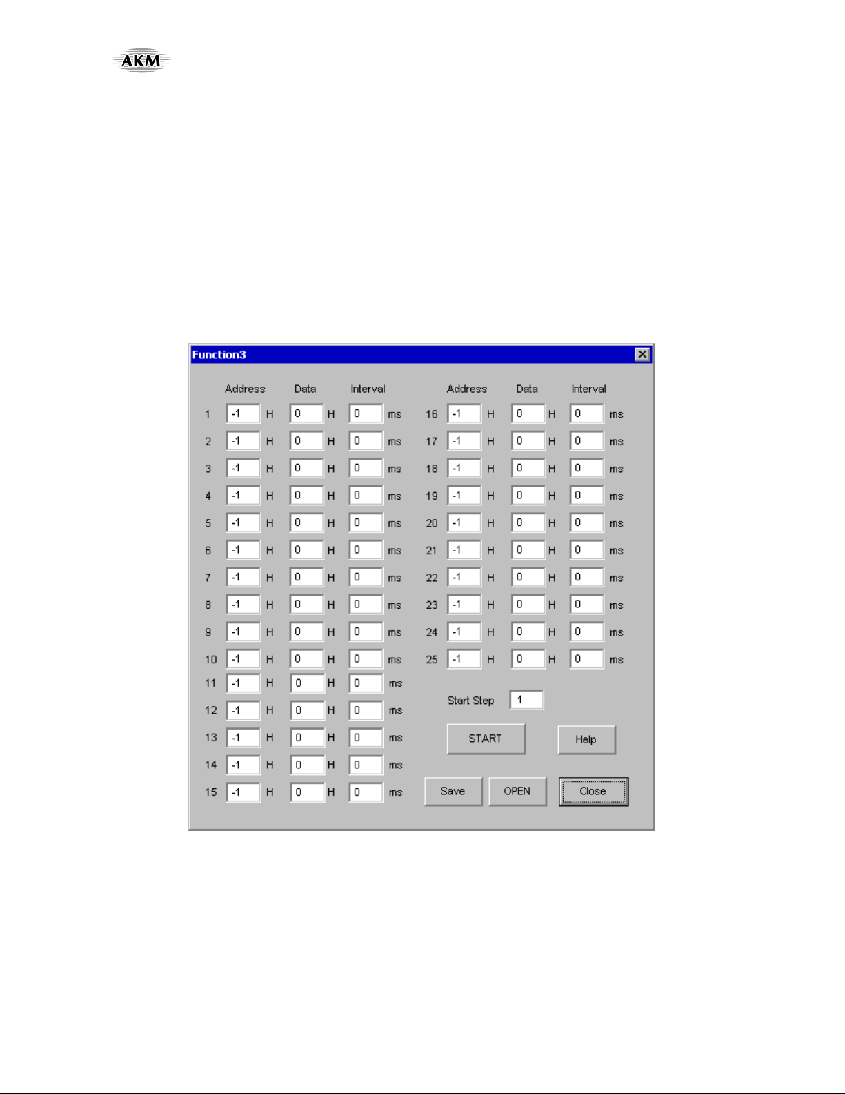
2. [Function1 Dialog]: Dialog to write data by keyboard operation
Address Box: Input registers address in 2 figures of hexadecimal.
Data Box: Input registers data in 2 figures of hexadecimal.
If you want to write the input data to AK5366, click [OK] button. If not, click [Cancel] button.
3. [Function2 Dialog]: Dialog to evaluate IPGA, DATT
This is a dialog corresponding to address: 04H, 05H, 08H, and 09H.
Address Box: Input registers address in 2 figures of hexadecimal.
Start Data Box: Input starts data in 2 figures of hexadecimal.
End Data Box: Input end data in 2 figures of hexadecimal.
Interval Box: Data is written to AK5366 by this interval.
Step Box: Data changes by this step.
Mode Select Box:
*If you check this check box, data reaches end data, and returns to start data.
[Example] Start Data = 00, End Data = 09
Data flow: 00 01 02 03 04 05 06 07 08 09 09 08 07 06 05 04 03 02 01 00
*If you do not check this check box, data reaches end data, but does not return to start data.
[Example] Start Data = 00, End Data = 09
Data flow: 00 01 02 03 04 05 06 07 08 09
If you want to write the input data to AK5366, click [OK] button. If not, click [Cancel] button.

[AKD5366]
<KM073601> 2007/04
- 9 -
4. [Save] and [Open]
4-1. [Save]
Save the current register setting data. The extension of file name is “akr”.
(Operation flow)
(1) Click [Save] Button.
(2) Set the file name and push [Save] Button. The extension of file name is “akr”.
4-2. [Open]
The register setting data saved by [Save] is written to AK5366. The file type is the same as [Save].
(Operation flow)
(1) Click [Open] Button.
(2) Select the file (*.akr) and Click [Open] Button.

[AKD5366]
<KM073601> 2007/04
- 10 -
5. [Function3 Dialog]
The sequence of register setting can be set and executed.
(1) Click [F3] Button.
(2) Set the control sequence.
Set the address, Data and Interval time. Set “-1” to the address of the step where the sequence should be paused.
(3) Click [Start] button. Then this sequence is executed.
The sequence is paused at the step of Interval="-1". Click [START] button, the sequence restarts from the paused step.
This sequence can be saved and opened by [Save] and [Open] button on the Function3 window. The extension of file name
is “aks”.
Figure 4. Window of [F3]

[AKD5366]
<KM073601> 2007/04
- 11 -
6. [Function4 Dialog]
The sequence that is created on [Function3] can be assigned to buttons and executed. When [F4] button is clicked, the
window as shown in Figure opens.
Figure 5. [F4] window

[AKD5366]
<KM073601> 2007/04
- 12 -
6-1. [OPEN] buttons on left side and [START] buttons
(1) Click [OPEN] button and select the sequence file (*.aks).
The sequence file name is displayed as shown in Figure.
Figure 6. [F4] window (2)
(2) Click [START] button, then the sequence is executed.
6-2. [SAVE] and [OPEN] buttons on right side
[SAVE]: The sequence file names can assign be saved. The file name is *.ak4.
[OPEN]: The sequence file names assign that are saved in *.ak4 are loaded.
6-3. Note
(1) This function doesn't support the pause function of sequence function.
(2) All files need to be in same folder used by [SAVE] and [OPEN] function on right side.
(3) When the sequence is changed in [Function3], the file should be loaded again in order to reflect the change.

[AKD5366]
<KM073601> 2007/04
- 13 -
7. [Function5 Dialog]
The register setting that is created by [SAVE] function on main window can be assigned to buttons and executed. When
[F5] button is clicked, the following window as shown in Figure opens.
Figure 7. [F5] window
7-1. [OPEN] buttons on left side and [WRITE] button
(1) Click [OPEN] button and select the register setting file (*.akr).
(2) Click [WRITE] button, then the register setting is executed.
7-2. [SAVE] and [OPEN] buttons on right side
[SAVE]: The register setting file names assign can be saved. The file name is *.ak5.
[OPEN]: The register setting file names assign that are saved in *.ak5 are loaded.
7-3. Note
(1) All files need to be in same folder used by [SAVE] and [OPEN] function on right side.
(2) When the register setting is changed by [Save] Button in main window, the file should be loaded again in order to
reflect the change.

[AKD5366]
<KM073601> 2007/04
- 14 -
MEASUREMENT RESULTS
[Measurement condition]
•Measurement unit: Audio Precision, System Two Cascade
•MCLK : 256fs
•BICK :64fs
•fs :48kHz
•Bit : 24bit
•Power Supply : AVDD = TVDD = 5.0V, DVDD = 3.3V
•Interface : DIT
•Temperature : Room
•External Condition : Input resistor (Ri) = 47kΩ, Feedback resistor (Rf) = 24kΩ
•IPGA Gain : 0dB
Parameter Result (Lch / Rch) Unit
Pre-Amp Characteristics:
S/(N+D) 103.9 / 103.5 dB
S/N (A-weighted) 107.9 / 107.6 dB
ADC Analog Input Characteristics: LIN1/RIN1 →Pre-Amp →IPGA →ADC, IPGA=0dB, ALC=OFF
S/(N+D) (-0.5dB Input) fs=48kHz 95.6 / 95.1 dB
D-Range (-60dB Input) fs=48kHz, A-weighted 102.6 / 102.4 dB
S/N fs=48kHz, A-weighted 102.6 / 102.4 dB
Interchannel Isolation 112.9 / 112.1 dB

[AKD5366]
<KM073601> 2007/04
- 15 -
[ADC Plot : fs=48kHz]
AKM AK5366 THD+Nvs. Input Level
AVDD=TVDD=5.0V, DVDD=3.3V, fs=48kHz, fin=1kHz
-120
-70
-115
-110
-105
-100
-95
-90
-85
-80
-75
d
B
F
S
-120 -10-110 -100 -90 -80 -70 -60 -50 -40 -30 -20
dBr
Figure 1. THD+N vs. Input Level
AKM AK5366 THD+Nvs. Input Frequency
AVDD=TVDD=5.0V, DVDD=3.3V, fs=48kHz, Input=-0.5dBr
-120
-70
-115
-110
-105
-100
-95
-90
-85
-80
-75
d
B
F
S
20 20k50 100 200 500 1k 2k 5k 10k
Hz
Figure 2. THD+N vs. Input Frequency

[AKD5366]
<KM073601> 2007/04
- 16 -
AKM AK5366 Linearity
AVDD=TVDD=5.0V, DVDD=3.3V, fs=48kHz, fin=1kHz
-140
+0
-130
-120
-110
-100
-90
-80
-70
-60
-50
-40
-30
-20
-10
d
B
F
S
-140 +0-130 -120 -110 -100 -90 -80 -70 -60 -50 -40 -30 -20 -10
dBr
Figure 3. Linearity
AKM AK5366 FrequencyResponse
AVDD=TVDD=5.0V, DVDD=3.3V, fs=48kHz, Input=-0.5dBr
-1
+0
-0.9
-0.8
-0.7
-0.6
-0.5
-0.4
-0.3
-0.2
-0.1
d
B
F
S
20 20k50 100 200 500 1k 2k 5k 10k
Hz
Figure 4. Frequency Response

[AKD5366]
<KM073601> 2007/04
- 17 -
AKM AK5366 Crosstalk
AVDD=TVDD=5.0V, DVDD=3.3V, fs=48kHz, Input=-0.5dBr
-140
-70
-135
-130
-125
-120
-115
-110
-105
-100
-95
-90
-85
-80
-75
d
B
20 20k50 100 200 500 1k 2k 5k 10k
Hz
Figure 5. Crosstalk
AKM AK5366 FFT Plot
AVDD=TVDD=5.0V, DVDD=3.3V, fs=48kHz, Input=-0.5dBr, fin=1kHz
-180
+0
-170
-160
-150
-140
-130
-120
-110
-100
-90
-80
-70
-60
-50
-40
-30
-20
-10
d
B
F
S
20 20k50 100 200 500 1k 2k 5k 10k
Hz
Figure 6. FFT Plot

[AKD5366]
<KM073601> 2007/04
- 18 -
AKM AK5366 FFT Plot
AVDD=TVDD=5.0V, DVDD=3.3V, fs=48kHz, Input=-60dBr, fin=1kHz
-180
+0
-170
-160
-150
-140
-130
-120
-110
-100
-90
-80
-70
-60
-50
-40
-30
-20
-10
d
B
F
S
20 20k50 100 200 500 1k 2k 5k 10k
Hz
Figure 7. FFT Plot
AKM AK5366 FFT Plot
AVDD=TVDD=5.0V, DVDD=3.3V, fs=48kHz, fin=None
-180
+0
-170
-160
-150
-140
-130
-120
-110
-100
-90
-80
-70
-60
-50
-40
-30
-20
-10
d
B
F
S
20 20k50 100 200 500 1k 2k 5k 10k
Hz
Figure 8. FFT Plot

[AKD5366]
<KM073601> 2007/04
- 19 -
Revision History
Date
(yy/mm/dd) Manual
Revision Board
Revision Reason Contents
04/05/25 KM073600 0 First Edition
Circuit Change Condenser Capacitance Value Change: C32, C33: Open5p07/04/23 KM073601 1 Change Control Software Manual Change
IMPORTANT NOTICE
These products and their specifications are subject to change without notice.
When you consider any use or application of these products, please make inquiries the sales office of Asahi Kasei EMD
Corporation (AKEMD) or authorized distributors as to current status of the products.
AKEMD assumes no liability for infringement of any patent, intellectual property, or other rights in the application or use of any
information contained herein.
Any export of these products, or devices or systems containing them, may require an export license or other official approval under the
law and regulations of the country of export pertaining to customs and tariffs, currency exchange, or strategic materials.
AKEMD products are neither intended nor authorized for use as critical componentsNote1) in any safety, life support, or other hazard
related device or systemNote2), and AKEMD assumes no responsibility for such use, except for the use approved with the express
written consent by Representative Director of AKEMD. As used here:
Note1) A critical component is one whose failure to function or perform may reasonably be expected to result, whether directly
or indirectly, in the loss of the safety or effectiveness of the device or system containing it, and which must therefore meet very
high standards of performance and reliability.
Note2)A hazard related device or system is one designed or intended for life support or maintenanceof safetyor for applications
in medicine, aerospace, nuclear energy, or other fields, in which its failure to function or perform may reasonably be expected to
result in loss of life or in significant injury or damage to person or property.
It is the responsibility of the buyer or distributor of AKEMD products, who distributes, disposes of, or otherwise places the product
with a third party, to notify such third party in advance of the above content and conditions, and the buyer or distributor agrees to
assume any and all responsibility and liability for and hold AKEMD harmless from any and all claims arising from the use of said
product in the absence of such notification.

A
A
B
B
C
C
D
D
E
E
E E
D D
C C
B B
A A
Title
Size Document Number Rev
Date: Sheet of
AK5366
1
AKD5366-Rev.A-44LQFP
A3
11Monday, December 18, 2006
Title
Size Document Number Rev
Date: Sheet of
AK5366
1
AKD5366-Rev.A-44LQFP
A3
11Monday, December 18, 2006
Title
Size Document Number Rev
Date: Sheet of
AK5366
1
AKD5366-Rev.A-44LQFP
A3
11Monday, December 18, 2006
+
C3
4.7u
+
C3
4.7u
+
C9
10u
+
C9
10u
C5
0.1u
C5
0.1u
R8
47k
R8
47k
1
2
3
4
5
6
7
8
9
10
11
12
CN3CN3
R4
47k
R4
47k
R7
47k
R7
47k
C4
0.1u
C4
0.1u
R11
47k
R11
47k
R2
47k
R2
47k
R12
24k
R12
24k
13
14
15
16
17
18
19
20
21
22
23
24
CN4CN4
R5
47k
R5
47k
R10
10
R10
10
LIN5
1
TEST1
2
LIN4
3
TEST2
4
LIN3
5
TEST3
6
LIN2
7
TEST4
8
LIN1
9
LOPIN
10
LOUT
11
IPGAL
12
IPGAR
13
ROUT
14
ROPIN
15
AVDD
16
AVSS
17
VCOM
18
DVSS
19
DVDD
20
SDTO
21
BICK
22
LRCK 23
MCLK 24
PDN 25
TVDD 26
SMUTE 27
SEL0 28
SEL1 29
SEL2 30
CDTI/SDA 31
CCLK/SCL 32
CSN/CAD1 33
I2C 34
M/S 35
RIN1 36
TEST5 37
RIN2 38
TEST6 39
RIN3 40
TEST7 41
RIN4 42
TEST8 43
RIN5 44
U1
AK5366
U1
AK5366
R13
24k
R13
24k
R1
47k
R1
47k
25
26
27
28
29
30
31
32
33
34
35
36
CN2CN2
R3
47k
R3
47k
R9
47k
R9
47k
+
C7
10u
+
C7
10u
+
C8
2.2u
+
C8
2.2u
+
C2
4.7u
+
C2
4.7u
R6
47k
R6
47k
C1
0.1u
C1
0.1u
37
38
39
40
41
42
43
44
45
46
47
48
CN1CN1
C6
0.1u
C6
0.1u
This manual suits for next models
1
Table of contents
Other AKM Motherboard manuals