AKM AKD4344-A User manual

[AKD4344-A]
<KM087902> 2007/07
- 1 -
GENERAL DESCRIPTION
The AKD4344-A is an evaluation board for the AK4344, 24bit and 96kHz DAC with DIT for portable and
home audio systems. The AKD4344-A has the interface with AKM’s A/D converter evaluation boards and
the interface with digital audio systems via optical connector. Therefore, it is easy to evaluate the
AK4344.
Ordering guide
AKD4344-A --- AK4344 Evaluation Board
FUNCTION
•Compatible with 2 types of input data interface
- Direct interface with AKM’s A/D converter evaluation boards via 10-pin header
- On-board AK4112B as DIR, which accepts optical or BNC Inputs
•Optical output for internal DIT
•BNC connector for an external clock input
•BNC connector for DAC output
VDD AGND
OPT
LOUT
ROUT
AK4112B
(DIR)
MCLK
OPT
Clock
Divider
Generator
Digital In Digital Out
74LVC541
10pin Header
DSP Data
VCCDGND
BNC Analog Out
AK4344
Figure 1. AKD4344-A Block Diagram
* Circuit diagram and PCB layout are attached at the end of this manual.
A
K4344 Evaluation Board Rev.2
A
KD4344-
A

[AKD4344-A]
<KM087902> 2007/07
- 2 -
Operation sequence
1) Set up the power supply lines.
[VDD] (Red) = 2.7 ∼3.6V (typ. 3.3V, for AK4344)
[VCC] (Red) = 2.7 ∼3.6V (typ. 3.3V, for AK4112B, for 74LVC541 and for logic)
[AGND] (Black) = 0V
[DGND] (Black) = 0V
Each supply line should be distributed from the power supply unit.
2) Set-up the evaluation modes, jumper pins and DIP switches (See the followings.)
3) Power on.
When AK4112B is used, The AK4112B and AK4344 should be reset once by bringing SW2 and SW1 “L”
upon power-up.
When AK4112B is not used, keep SW2 to “L”, and the AK4344 should be reset once by bringing SW1 “L”
upon power-up.
Evaluation mode
1) D/A part evaluation using optical or S/PDIF input <Default>
Use PORT1 (RX1: OPT) or J2 (RX1: BNC).
The AK4112B (DIR) generates MCLK, BICK, LRCK and SDTI1 from the received data through Optical
connector (TORX141) or BNC connector. This evaluation mode should be used for the evaluation using CD test
disk. Nothing should be connected to PORT3 (DSP). The selection of OPT and BNC should be done by JP14
(RX1)
JP7
LRCK
JP4
MCLK JP12
EXT
DI
R
EXT
DI
R
EX
T
JP5
BICK
DI
R
EX
T
JP6
SDTI1
2) D/A part evaluation using 10-pin connector on the AKM’s A/D evaluation board
Use PORT3 (DSP).
It is able to evaluate the AK4344, connecting the 10-pin connector on the AKM’s A/D evaluation board and
PORT3 (DSP) via 10-line flat cable.MCLK, BICK, LRCK and SDTI1 are sent from the A/D converter evaluation
board to the AKD4344 through PORT3 (DSP) via 10-line flat cable.
JP7
LRCK
JP4
MCLK JP12
EXT
DI
R
EXT
DI
R
EX
T
JP5
BICK
DI
R
EXT
JP6
SDTI1
3) D/A part evaluation using PORT3 (DSP), and supplying all interface signals from external equipments
In case of using PORT3 (DSP), and supplying signals (MCLK, BICK, LRCK, SDTI1) that is needed for
the AK4344 from external equipments, set up as following.
JP7
LRCK
JP4
MCLK JP12
EXT
DI
R
EXT
DI
R
EX
T
JP5
BICK
DI
R
EXT
JP6
SDTI1
In case of using PORT3 (DSP), and supplying SDTI2 from external equipments, setting of SDTI2
should be done by JP8 (SDTI2).

[AKD4344-A]
<KM087902> 2007/07
- 3 -
Other Jumper pins set up
(1) JP15 (VDD): VDD and VCC
OPEN: Separated
SHORT: Common. (The connector “VCC” can be open.) <Default>
By opening the connector “VCC”, shorting JP15 (VDD) and supplying 3.3V to the connector “VDD”, the
connector “VDD” can supply 3.3V to all circuits
(2) JP16 (GND): Analog ground and Digital ground
OPEN: Separated
SHORT: Common. (The connector “DGND” can be open.) <Default>
(3) JP10 (BCFS): Select the BICK of the AK4344
x1: BICK=128fs in case of MCLK=256fs/384fs/512fs/768fs.
BICK=64fs in case of MCLK=192fs.
x2: BICK=64fs in case of MCLK=128fs/256fs/384fs/512fs/768fs. <Default>
BICK=32fs in case of MCLK=192fs.
BICK=128fs in case of MCLK=1024fs/1536fs.
x4: BICK=32fs in case of MCLK=128fs/256fs/384fs/512fs/768fs.
BICK=64fs in case of MCLK=1024fs/1536fs.
x8: BICK=32fs in case of MCLK=1024fs/1536fs.
(4) JP11 (DIV), [JP9] (CLK), [JP13] (LRFS)
When using J1 (EXT), these jumper pins should be set according to Table 1.
(5) JP2 (CDTO / SDTI2): Select the signal of CDTO / SDTI2 pin
CDTO: Select the CDTO<Default>
SDTI2: Select the SDTI2
(6) JP8 (SDTI2): Select the input of SDTI2 pin
PORT3:Input the signal from PORT3
GND: Input the “0” Data <Default>
(When JP2 (CDTO / SDTI2): setting is CDTO, Set to GND)

[AKD4344-A]
<KM087902> 2007/07
- 4 -
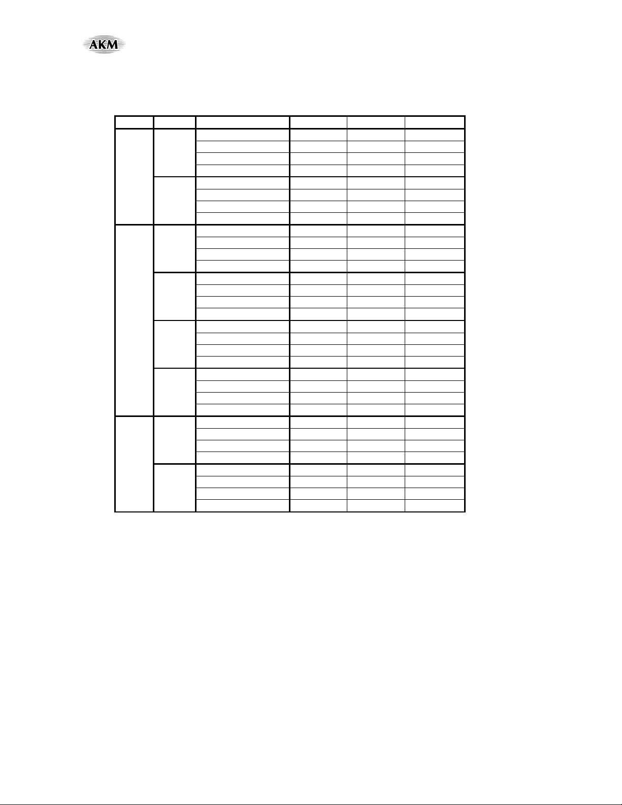
Example for External Clock setting
Refer to the following setting when MCLK, BICK and LRCK are supplied to the AK4344 from J1 (EXT).
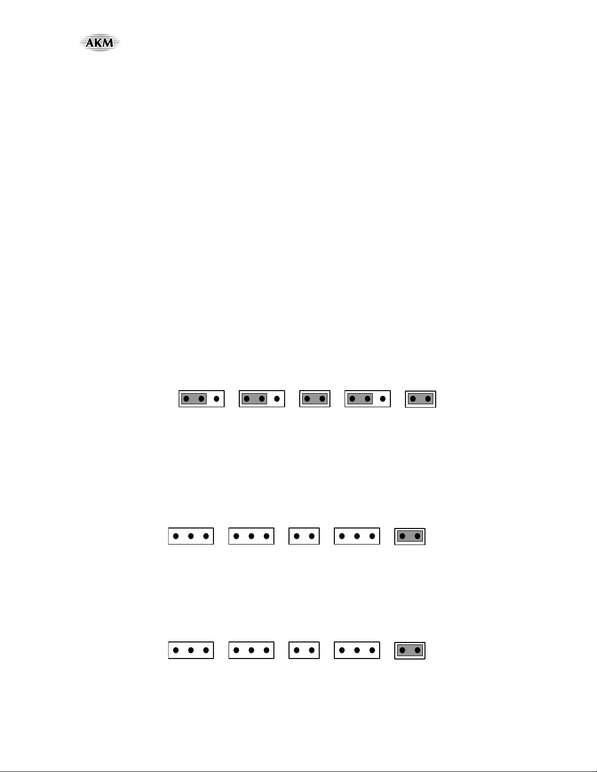
Mode fs MCLK JP11 (DIV) JP9 (CLK) JP13 (LRFS)
512fs = 4.096MHz x2 x2 x1
768fs = 6.144MHz x3 x2 x1
1024fs = 8.192MHz x2 x2 x2
8kHz
1536fs = 12.288MHz x3 x2 x2
512fs = 12.288MHz x2 x2 x1
768fs = 18.432MHz x3 x2 x1
1024fs = 24.576MHz x2 x2 x2
Half
24kHz
1536fs = 36.864MHz x3 x2 x2
256fs = 2.048MHz x1 x2 x1
384fs = 3.072MHz OPEN x3 x1
512fs = 4.096MHz x2 x2 x1
8kHz
768fs = 6.144MHz x3 x2 x1
256fs = 8.192MHz x1 x2 x1
384fs = 12.288MHz OPEN x3 x1
512fs = 16.384MHz x2 x2 x1
32kHz
768fs = 24.576MHz x3 x2 x1
256fs = 11.2896MHz x1 x2 x1 Default
384fs = 16.9344MHz OPEN x3 x1
512fs = 22.5792MHz x2 x2 x1
44.1kHz
768fs = 33.8688MHz x3 x2 x1
256fs = 12.288MHz x1 x2 x1
384fs = 18.432MHz OPEN x3 x1
512fs = 24.576MHz x2 x2 x1
Normal
48kHz
768fs = 36.864MHz x3 x2 x1
128fs = 6.144MHz OPEN x1 x1
192fs = 9.216MHz OPEN x3 x3
256fs = 12.288MHz x1 x2 x1
48kHz
384fs = 18.432MHz OPEN x3 x1
128fs = 12.288MHz OPEN x1 x1
192fs = 18.432MHz OPEN x3 x3
256fs = 24.576MHz x1 x2 x1
Double
96kHz
384fs = 36.864MHz OPEN x3 x1
Table 1. Clock Setting

[AKD4344-A]
<KM087902> 2007/07
- 5 -
DIP Switch set up
[SW3]: Setting the audio data format of the AK4112B (ON=“H”, OFF=“L”)
Mode SW3-3
DIF2 SW3-2
DIF1 SW3-1
DIF0 SDTI Format
0 L L L 16bit, LSB justified
3 L H H 24bit, LSB justified
4 H L L 24bit, MSB justified
5 H L H 24bit, I2S Compatible Default
Table 2. SW3: Audio Data Format of AK4112B
Note. The AK4112B does not support 16bit, I2S Compatible.

[AKD4344-A]
<KM087902> 2007/07
- 6 -
The function of the toggle SW
[SW1] (AK4344-PDN): Resets the AK4344. Keep “H” during normal operation.
The AK4344 should be reset once by bringing SW1 “L” upon power-up.
[SW2] (AK4112B-PDN): Resets the AK4112B. Keep “H” during normal operation.
The AK4112B should be reset once by bringing SW2 “L” upon power-up.
Analog Output Circuit
The DAC of AK4344 outputs analog audio signals through J3 and J4.
+
C13
22u R7
220
J3
BNC-R-PC
1 2
3
4
5
R9
10k
+
C17
22u
R13
10k
R12
220
J4
BNC-R-PC
1 2
3
4
5
C100
1n
C101
1n
LOU
T
ROU
T
AK4344-LOUT
AK4344-ROUT
Figure 2. LOUT/ROUT Output circuit
* AKEMD assumes no responsibility for the trouble when using the above circuit examples.
Serial control
The AKD4344-A can be controlled via the printer port (parallel port) of IBM-AT compatible PC. Connect PORT4
(uP-I/F) to PC by 10-line flat cable packed with the AKD4344-A. Take care of the direction of connector. There is a
mark at pin#1. The pin layout of PORT4 as shown Figure 3.
PORT4
uP I/F 10
9
2
1
NC
CDTO
CDTI
CCL
K
CSN
GND
GND
GND
GND
GND
Red
Figure 3. PORT4 pin layout

[AKD4344-A]
<KM087902> 2007/07
- 7 -
Control Software Manual
Set-up of evaluation board and control software
1.Set up the AKD4344-A according to the Operating Sequence located on page 2.
2.Connect IBM-AT compatible PC with AKD4344-A by 10-line type flat cable (packed with AKD4344-A). Take care
of the direction of 10pin header. (Please install the driver in the CD-ROM when this control software is used on
Windows 2000/XP. Please refer “Installation Manual of Control Software Driver by AKM device control software”.
In case of Windows95/98/ME, this installation is not needed. This control software does not operate on Windows
NT.)
3.Insert the CD-ROM labeled “AKD4344-A Evaluation Kit” into the CD-ROM drive.
4.Access the CD-ROM drive and double-click the icon of “akd4344-a.exe” to set up the control program.
5.Please evaluate according to the following.
Operation flow
Keep the following flow.
1. Set up the control program according to explanation above.
2. Click “Port Reset” button.
Explanation of each buttons
1. [Port Reset]: Set up the USB interface board (AKDUSBIF-A).
2. [Write default]: Initialize the register of AK4344.
3. [All Write]: Write all registers that is currently displayed.
4. [Function1]: Dialog to write data by keyboard operation.
5. [Function2]: Dialog to write data by keyboard operation.
6. [Function3]: The sequence of register setting can be set and executed.
7. [Function4]: The sequence that is created on [Function3] can be assigned to buttons and executed.
8. [Function5]: The register setting that is created by [SAVE] function on main window can be assigned to
buttons and executed.
9. [SAVE]: Save the current register setting.
10. [OPEN]: Write the saved values to all register.
11. [Write]: Dialog to write data by mouse operation.
Indication of data
Input data is indicated on the register map. Red letter indicates “H” or “1” and blue one indicates “L” or “0”. Blank is the
part that is not defined in the datasheet.

[AKD4344-A]
<KM087902> 2007/07
- 8 -
Explanation of each dialog
1. [Write Dialog]: Dialog to write data by mouse operation
There are dialogs corresponding to each register.
Clickthe [Write] button corresponding to each register to set up the dialog. If you check the check box, data becomes
“H” or “1”. If not, “L” or “0”.
If you want to write the input data to AK4344, click [OK] button. If not, click [Cancel] button.
2. [Function1 Dialog] : Dialog to write data by keyboard operation
Address Box: Input registers address in 2 figures of hexadecimal.
Data Box: Input registers data in 2 figures of hexadecimal.
If you want to write the input data to AK4344, click [OK] button. If not, click [Cancel] button.
3. [Function2 Dialog] : Dialog to evaluate ATT
Address Box: Input registers address in 2 figures of hexadecimal.
Start Data Box: Input starts data in 2 figures of hexadecimal.
End Data Box: Input end data in 2 figures of hexadecimal.
Interval Box: Data is written to AK4344 by this interval.
Step Box: Data changes by this step.
Mode Select Box:
*If you check this check box, data reaches end data, and returns to start data.
[Example] Start Data = 00, End Data = 09
Data flow: 00 01 02 03 04 05 06 07 08 09 09 08 07 06 05 04 03 02 01 00
*If you do not check this check box, data reaches end data, but does not return to start data.
[Example] Start Data = 00, End Data = 09
Data flow: 00 01 02 03 04 05 06 07 08 09
If you want to write the input data to AK4344, click [OK] button. If not, click [Cancel] button.

[AKD4344-A]
<KM087902> 2007/07
- 9 -
4. [Save] and [Open]
4-1. [Save]
Save the current register setting data. The extension of file name is “akr”.
(Operation flow)
(1) Click [Save] Button.
(2) Set the file name and push [Save] Button. The extension of file name is “akr”.
4-2. [Open]
The register setting data saved by [Save] is written to AK4344. The file type is the same as [Save].
(Operation flow)
(1) Click [Open] Button.
(2) Select the file (*.akr) and Click [Open] Button.

[AKD4344-A]
<KM087902> 2007/07
- 10 -
5. [Function3 Dialog]
The sequence of register setting can be set and executed.
(1) Click [F3] Button.
(2) Set the control sequence.
Set the address, Data and Interval time. Set “-1” to the address of the step where the sequence should be paused.
(3) Click [Start] button. Then this sequence is executed.
The sequence is paused at the step of Interval="-1". Click [START] button, the sequence restarts from the paused step.
This sequence can be saved and opened by [Save] and [Open] button on the Function3 window. The extension of file name
is “aks”.
Figure 4. Window of [F3]

[AKD4344-A]
<KM087902> 2007/07
- 11 -
6. [Function4 Dialog]
The sequence that is created on [Function3] can be assigned to buttons and executed. When [F4] button is clicked, the
window as shown in Figure opens.
Figure 5. [F4] window

[AKD4344-A]
<KM087902> 2007/07
- 12 -
6-1. [OPEN] buttons on left side and [START] buttons
(1) Click [OPEN] button and select the sequence file (*.aks).
The sequence file name is displayed as shown in Figure.
Figure 6. [F4] window(2)
(2) Click [START] button, then the sequence is executed.
6-2. [SAVE] and [OPEN] buttons on right side
[SAVE]: The sequence file names can assign be saved. The file name is *.ak4.
[OPEN]: The sequence file names assign that are saved in *.ak4 are loaded.
6-3. Note
(1) This function doesn't support the pause function of sequence function.
(2) All files need to be in same folder used by [SAVE] and [OPEN] function on right side.
(3) When the sequence is changed in [Function3], the file should be loaded again in order to reflect the change.

[AKD4344-A]
<KM087902> 2007/07
- 13 -
7. [Function5 Dialog]
The register setting that is created by [SAVE] function on main window can be assigned to buttons and executed. When
[F5] button is clicked, the following window as shown in Figure opens.
Figure 7. [F5] window
7-1. [OPEN] buttons on left side and [WRITE] button
(1) Click [OPEN] button and select the register setting file (*.akr).
(2) Click [WRITE] button, then the register setting is executed.
7-2. [SAVE] and [OPEN] buttons on right side
[SAVE] : The register setting file names assign can be saved. The file name is *.ak5.
[OPEN] : The register setting file names assign that are saved in *.ak5 are loaded.
7-3. Note
(1) All files need to be in same folder used by [SAVE] and [OPEN] function on right side.
(3) When the register setting is changed by [Save] Button in main window, the file should be loaded again in order to
reflect the change.

[AKD4344-A]
<KM087902> 2007/07
- 14 -
MEASUREMENT RESULTS
[Measurement condition]
•Measurement unit : Audio Precision, System Two Cascade
•MCLK : 512fs (fs=44.1KHz) / 256fs (fs=96KHz)
•BICK :64fs
•fs : 44.1kHz / 96kHz
•BW : 20Hz~20KHz (fs=44.1kHz) / 20Hz~40KHz (fs=96kHz)
•Bit : 24bit
•Power Supply : VDD = 3.3V
•Interface : PSIA
•Temperature : Room
[Measurement Results]
Parameter Results Unit
DAC Analog Output Characteristics Lch / Rch
S/(N+D)
(fs=44.1kHz, fin=1KHz, 0dBFS)
(fs=96kHz, fin=1KHz, 0dBFS)
-91.2/-91.2
-89.0/-89.1
dB
dB
D-Range
(fs=44.1kHz, fin=1KHz, -60dBFS, A-weighted)
(fs=96kHz, fin=1KHz, -60dBFS, A-weighted)
99.4/99.4
99.4/99.4
dB
dB
S/N
(fs=44.1kHz, no-input, A-weighted)
(fs=96kHz, no-input, A-weighted)
99.6/99.5
99.4/99.4
dB
dB
Interchannel Isolation (fin=1KHz, 0dBFS/ no-input) 115.0/115.2 dB

[AKD4344-A]
<KM087902> 2007/07
- 15 -
[DACPlot:fs=44.1kHz]
AKM 06/18/07 09:30:43THD+Nvs. Input Level
fs=44.1kHz, fin=1kHz
-100
-70
-98
-96
-94
-92
-90
-88
-86
-84
-82
-80
-78
-76
-74
-72
d
B
r
A
-140 +0-130 -120 -110 -100 -90 -80 -70 -60 -50 -40 -30 -20 -10
dBFS
Figure1.THD+Nvs.InputLevel(fin=1KHz)
AKM 06/18/07 09:28:48THD+N vs. Input Freqency
fs=44.1kHz, fin=0dBFs
-100
-70
-98
-96
-94
-92
-90
-88
-86
-84
-82
-80
-78
-76
-74
-72
d
B
r
A
20 20k50 100 200 500 1k 2k 5k 10k
Hz
Figure2.THD+Nvs.InputFrequency(InputLevel=0dBFS)

[AKD4344-A]
<KM087902> 2007/07
- 16 -
[DACPlot:fs=44.1kHz]
AKM 06/18/07 09:35:13Linearity
fs=44.1kHz, fin=1kHz
-140
+0
-130
-120
-110
-100
-90
-80
-70
-60
-50
-40
-30
-20
-10
d
B
r
A
-140 +0-130 -120 -110 -100 -90 -80 -70 -60 -50 -40 -30 -20 -10
dBFS
Figure3.Linearity(fin=1KHz)
AKM 06/18/07 09:49:36FreqencyResponse
fs=44.1kHz, fin=0dBFs
-1
+1
-0.9
-0.8
-0.7
-0.6
-0.5
-0.4
-0.3
-0.2
-0.1
+0
+0.1
+0.2
+0.3
+0.4
+0.5
+0.6
+0.7
+0.8
+0.9
d
B
r
A
2k 20k4k 6k 8k 10k 12k 14k 16k 18k
Hz
Figure4.FrequencyResponse(InputLevel=0dBFS)

[AKD4344-A]
<KM087902> 2007/07
- 17 -
[DACPlot:fs=44.1kHz]
AKM 06/18/07 09:56:53Crosstalk
fs=44.1kHz
-130
-70
-124
-118
-112
-106
-100
-94
-88
-82
-76
d
B
10 20k20 50 100 200 500 1k 2k 5k 10k
Hz
Figure5.Crosstalk(fin=1KHz,InputLevel=0dBFS/no-input)
AKM 06/18/07 10:07:31FFT
fs=44.1kHz, fin=0dBFs,1kHz
-160
+0
-150
-140
-130
-120
-110
-100
-90
-80
-70
-60
-50
-40
-30
-20
-10
d
B
r
A
10 20k20 50 100 200 500 1k 2k 5k 10k
Hz
Figure6.FFTPlot(fin=1KHz,InputLevel=0dBFS)

[AKD4344-A]
<KM087902> 2007/07
- 18 -
[DACPlot:fs=44.1kHz]
AKM 06/18/07 10:08:53FFT
fs=44.1kHz, fin=-60dBFs,1kHz
-160
+0
-150
-140
-130
-120
-110
-100
-90
-80
-70
-60
-50
-40
-30
-20
-10
d
B
r
A
10 20k20 50 100 200 500 1k 2k 5k 10k
Hz
Figure7.FFTPlot(fin=1KHz,InputLevel=−60dBFS)
AKM 06/18/07 10:09:30FFT Noise floor
fs=44.1kHz
-160
+0
-150
-140
-130
-120
-110
-100
-90
-80
-70
-60
-50
-40
-30
-20
-10
d
B
r
A
10 20k20 50 100 200 500 1k 2k 5k 10k
Hz
Figure8.FFTPlot(no-input)

[AKD4344-A]
<KM087902> 2007/07
- 19 -
[DACPlot:fs=96kHz]
AKM 06/18/07 10:32:35FFT Out-of-band Noise
fs=44.1kHz
-160
+0
-150
-140
-130
-120
-110
-100
-90
-80
-70
-60
-50
-40
-30
-20
-10
d
B
r
A
10 100k20 50 100 200 500 1k 2k 5k 10k 20k 50k
Hz
Figure9.FFTPlot(out-of-band-noise)
THD+NvsInputLevel
fs=96KHz,fin=1KHz
-120
-
70
-117.5
-115
-112.5
-110
-107.5
-105
-102.5
-100
-97.5
-95
-92.5
-90
-87.5
-85
-82.5
-80
-77.5
-75
-72.5
d
B
r
A
-140 +0-130 -120 -110 -100 -90 -80 -70 -60 -50 -40 -30 -20 -10
dBFS
Figure10.THD+Nvs.InputLevel(fin=1KHz)

[AKD4344-A]
<KM087902> 2007/07
- 20 -
[DACPlot:fs=96kHz] THD+NvsInputFrequency
fs=96KHz,InputLevel=0dBFS
-120
-
70
-117.5
-115
-112.5
-110
-107.5
-105
-102.5
-100
-97.5
-95
-92.5
-90
-87.5
-85
-82.5
-80
-77.5
-75
-72.5
d
B
r
A
10 40k20 50 100 200 500 1k 2k 5k 10k 20k
Hz
TTTT
Figure11.THD+Nvs.InputFrequency(InputLevel=0dBFS)
AKM 06/18/07 10:46:53Linearity
fs=96kHz
-140
+0
-130
-120
-110
-100
-90
-80
-70
-60
-50
-40
-30
-20
-10
d
B
r
A
-140 +0-130 -120 -110 -100 -90 -80 -70 -60 -50 -40 -30 -20 -10
dBFS
Figure12.Linearity(fin=1KHz)
Table of contents
Other AKM Motherboard manuals