AKM AK4686 User manual

[AKD4686-B]
A
K4686 Evaluation Board Rev.0
AKD4686-B
FEATURE
AKD4686-B is an evaluation board for AK4686, a single chip 24bit CODEC that has one stereo ADC and
two stereo DAC. This board has interfaces with AKM’s evaluation boards for A/D converter and D/A
converter and makes easy to evaluate AK4686. Also this board has the digital audio interface and then
achieves the interface with digital audio systems via RCA connector.
Ordering guide
AKD4686-B --- Evaluation Board for AK4686
(Cable for connecting with printer port of IBM-AT compatible PC and control
software are packed with this. This control software does not operate on Windows
NT.)
FUNCTION
On-board clock generators (AK4118 x 2)
Compatible with 2 types of digital audio interface
- RCA (S/PDIF) input/output
- 10pin headers for interfacing with external data source (x2)
RCA connectors for clock input with external clock source
10pin header for register control
GND
AK4686
+5V
Regulator
LOUT1/ROUT1
LOUT2/ROUT2
+3.3V
LIN / RIN
Control Data
10pin Header
RCA OUT
RCA IN
10pin Header
PORT 1
EX1
AK4118
(DIT/DIR)
EX2
10pin Header
PORT 2
AK4118
(DIR)
RCA IN
Figure 1. AKD4686-B Block Diagram
(* Circuit diagram and PCB layout are attached at the end of this manual.)
< KM103800> 2010/08
- 1 -

[AKD4686-B]
EVALUATION BOARD MANUAL
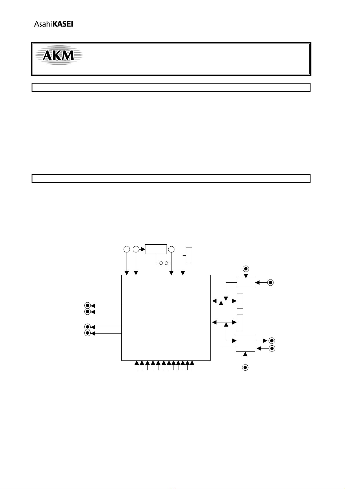
Operating sequence
1. Set up power supply lines.
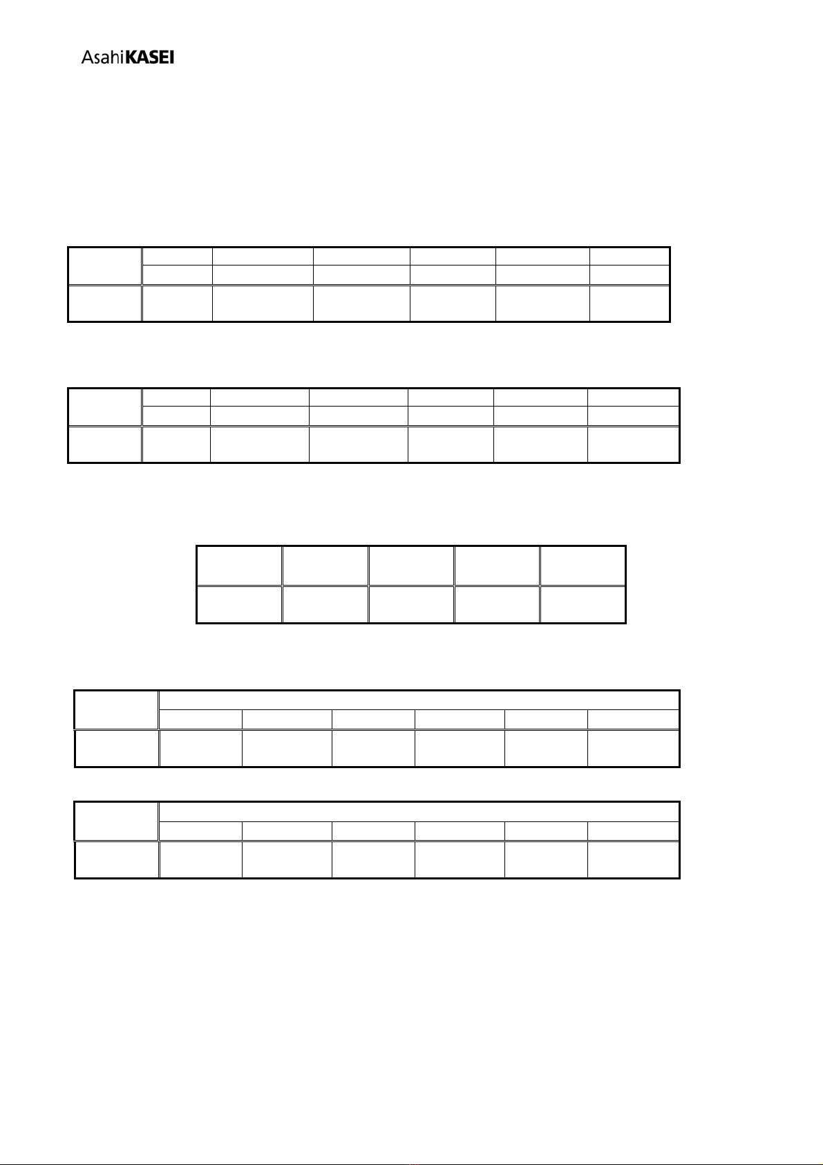
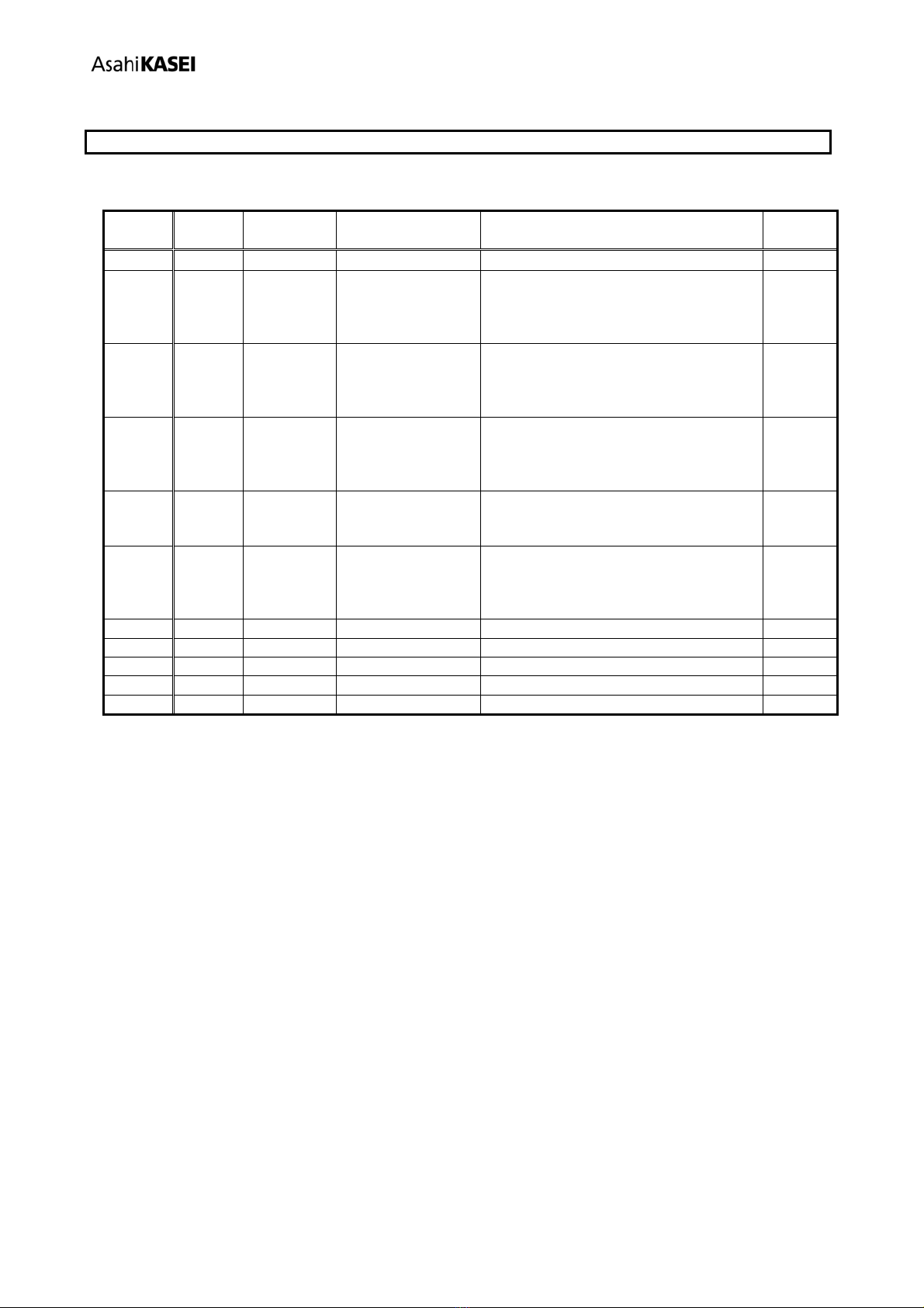
Name of
Jack
Color of
Jack Voltage Used for Comment and attention Default
+5V Red
+4.5∼+5.5V Regulator T2, T5 Should be always connected +5V
AVDD1 Orange +3.0∼+3.6V AVDD1 of AK4686
Should be open when JP40
(AVDD1_SEL) is set to REG side.
Should be connected when JP40
(AVDD1_SEL) is set to AVDD1 side.
Open
AVDD2 Orange +3.0∼+3.6V AVDD2 of AK4686
Should be open when JP41
(AVDD2_SEL) is set to REG side.
Should be connected when JP41
(AVDD2_SEL) is set to AVDD2 side.
Open
DVDD Orange
+3.0∼+3.6V DVDD of AK4686
Should be open when JP42 (DVDD_SEL)
is set to REG side.
Should be connected when JP42
(DVDD_SEL) is set to DVDD side.
Open
CVDD Orange
+3.0∼+3.6V CVDD of AK4686
Should be connected when default.
Should be open in case of using regulator
T2 when R85 is short and L7 is open.
+3.3V
D3.3V Orange
+3.0∼+3.6V Power supply of
logic
Should be open when JP45 (D3.3V_SEL)
is set to REG side.
Should be connected when JP45
(D3.3V_SEL) is set to D3.3V side.
Open
VSS1 Black 0V Analog Ground Should be always connected 0V
VSS2 Black 0V Analog Ground Should be always connected 0V
VSS3 Black 0V Analog Ground Should be always connected 0V
VSS4 Black 0V Analog Ground Should be always connected 0V
DGND Black 0V Digital Ground Should be always connected 0V
Table 1. Power supply lines
Each supply line should be distributed from the power supply unit.
2. Set up evaluation mode and jumper pins. (Refer to the following item.)
3. Connect cables. (Refer to the following item.)
4. Power on.
The AK4686 (U1) should be reset once bringing SW1 (PDN) “L” upon power-up.
Keep “H” during normal operaion.
5. Set up control software registers. (Refer to the following item.)
< KM103800> 2010/08
- 2 -

[AKD4686-B]
Evaluation modes
(1) DAC with external DIR (Synchronous mode)
1. Connection of connector
For digital (S/PDIF) input, RCA connectors J12 (PORT1 RX0) and J15 (PORT2 RX0) are available.
For analog output, RCA connectors J5 (LOUT1)/JP6 (ROUT1), J7 (LOUT2)/J8 (ROUT2) are available.
2. Setting of jumper pin
Setting of interface signal of PORT1: AK4118 (U4) is as follows.
JP19 JP20 JP21 JP22 JP23 JP50
Jumper XTI1 MCKO_SEL1 MCLK1_SEL BICK1_SEL LRCK1_SEL SDTI1
Setting Open MCKO1 Short Short Short Short (Default)
Table 2. Setting of interface signal of PORT1: AK4118 (U4) (1/3)
Setting of interface signal of PORT2: AK4118 (U7) is as follows.
JP26 JP27 JP28 JP29 JP30 JP31
Jumper XTI2 MCKO_SEL2 MCLK2_SEL BICK2_SEL LRCK2_SEL SDTI2_SEL
Setting Open Don’t care MCDIR1 BIDIR1 LRDIR1 SDDIR1
Table 3. Setting of interface signal of PORT2: AK4118 (U7) (1/3)
3. Setting of toggle switch
Switch SW2 SW5 SW6 SW7
Setting H L H H
Table 4. Setting of interface signal of PORT1, PORT2: AK4118 (U4,U7) (2/3)
4. Setting of DIP switch
SW3
Switch DIF0 DIF1 DIF2 CM0 OCKS0 OCKS1
Setting H L H L L H
Table 5. Setting of interface signal of PORT1: AK4118 (U4) (3/3)
SW4
Switch DIF0 DIF1 DIF2 CM0 OCKS0 OCKS1
Setting Don’t care Don’t care Don’t care Don’t care Don’t care Don’t care
Table 6. Setting of interface signal of PORT2: AK4118 (U7) (3/3)
< KM103800> 2010/08
- 3 -

[AKD4686-B]
(2) DAC with external DIR (Asynchronous mode)
1. Connection of connector
For digital (S/PDIF) input, RCA connectors J12 (PORT1 RX0) and J15 (PORT2 RX0) are available.
For analog output, RCA connectors J5 (LOUT1)/JP6 (ROUT1), J7 (LOUT2)/J8 (ROUT2) are available.
2. Setting of jumper pin
Setting of interface signal of PORT1: AK4118 (U4) is as follows.
JP19 JP20 JP21 JP22 JP23 JP50
Jumper XTI1 MCKO_SEL1 MCLK1_SEL BICK1_SEL LRCK1_SEL SDTI1
Setting Open MCKO1 Short Short Short Short (Default)
Table 7. Setting of interface signal of PORT1: AK4118 (U4) (1/3)
Setting of interface signal of PORT2: AK4118 (U7) is as follows.
JP26 JP27 JP28 JP29 JP30 JP31
Jumper XTI2 MCKO_SEL2 MCLK2_SEL BICK2_SEL LRCK2_SEL SDTI2_SEL
Setting Open MCKO1 MCDIR2 BIDIR2 LRDIR2 SDDIR2 (Default)
Table 8. Setting of interface signal of PORT2: AK4118 (U7) (1/3)
3. Setting of toggle switch
Switch SW2 SW5 SW6 SW7
Setting H H H H
Table 9. Setting of interface signal of PORT1, PORT2: AK4118 (U4, U7) (2/3)
4. Setting of DIP switch
SW3
Switch DIF0 DIF1 DIF2 CM0 OCKS0 OCKS1
Setting H L H L L H (Default)
Table 10. Setting of interface signal of PORT1: AK4118 (U4) (3/3)
SW4
Switch DIF0 DIF1 DIF2 CM0 OCKS0 OCKS1
Setting H L H L L H (Default)
Table 11. Setting of interface signal of PORT2: AK4118 (U7) (3/3)
< KM103800> 2010/08
- 4 -

[AKD4686-B]
(3) ADC with external DIT
1. Connection of connector
For analog input, RCA connector JL1(LIN1), JL2(LIN2), JL3(LIN3), JL4(LIN4), JL5(LIN5), JL6(LIN6) and
JR1(RIN1), JR2(RIN2), JR3(RIN3), JR4(RIN4), JR5(RIN5), JR6(RIN6) are available.
For digital (S/PDIF) output, RCA connector J13 (PORT1 TX1) is available.
2. Setting of jumper pin
Setting of interface signal of PORT1: AK4118 (U4) is as follows.
X1 (24.576MHz) is used as Clock (512fs) .
JP19 JP20 JP21 JP22 JP23 JP24
Jumper XTI1 MCKO1_SEL MCLK1_SEL BICK1_SEL LRCK1_SEL SDTO1_SEL
Setting Open MCKO1 Short Short Short Short (Default)
Table 12. Setting of interface signal of PORT1: AK4118 (U4) (1/3)
3. Setting of toggle switch
Switch SW2 SW5
Setting H L
Table 13. Setting of reset of PORT1 AK4118 (U4) (2/3)
4. Setting of DIP switch
SW3
Switch DIF0 DIF1 DIF2 CM0 OCKS0
OCKS1 MS1
Setting H L H H L H L
Table 14. Setting of interface signal of PORT1: AK4118 (U4) (3/3)
< KM103800> 2010/08
- 5 -

[AKD4686-B]
Register control
AKD4686-B can be controlled via the printer port (parallel port) of IBM-AT compatible PC. Connect PORT3
(uP-I/F) to PC by 10-line flat cable packed with this. Take care of the direction of connector.
SDA
SDA
(
ACK
)
SCL
AKD4686-B
10-pin header
10-pin connector10-wire flat cable
Connect
PC
RED
9
1
2
PORT3
UP-I/F
10
Figure 2. PORT1 pin layout
Set-up DIP switch (SW3, 4)
No. Name Content Default
SW3-1 DIF0 ON
SW3-2 DIF1 OFF
Setting of AK4118 Audio Interface Format
Table 16.)
(Refer
SW3-3 DIF2 ON
Selection of AK4118 Clock Mode (Clock Source)
SW3-4 CM0 OFF
Table 17.)
(Refer
SW3-6 OCKS0 OFF
SW3-7 OCKS1
Selection of AK4118 Master Clock Output frequency
Table 18.)(Refer ON
PORT1 Master Mode/Slave Mode Switch
SW3-8 MS1 OFF
(Refer to the AK4686’s datasheet)
SW4-1 DIF0 ON
SW4-2 DIF1 OFF
Setting of AK4118 Audio Interface Format
(Refer Table 16.)
SW4-3 DIF2 ON
Selection of AK4118 Clock Mode (Clock Source)
SW4-4 CM0 OFF
Table 17.)
(Refer
SW4-6 OCKS0 OFF
SW4-7 OCKS1
Selection of AK4118 Master Clock Output frequency
(Refer Table 18.) ON
Table 15. Set up modes of AK4118 (U4, U7) and AK4686 (U1)
LRCK BICK
Mode DIF2 DIF1 DIF0 DAUX SDTO I/O I/O
0 0 0 0 24bit, Left justified 16bit, Right justified H/L O 64fs O
1 0 0 1 24bit, Left justified 18bit, Right justified H/L O 64fs O
2 0 1 0 24bit, Left justified 20bit, Right justified H/L O 64fs O
3 0 1 1 24bit, Left justified 24bit, Right justified H/L O 64fs O
4 1 0 0 24bit, Left justified 24bit, Left justified H/L O 64fs O
5 1 0 1 24bit, I2S 24bit, I2S L/H O 64fs O <Default>
6 1 1 0 24bit, Left justified 24bit, Left justified H/L I 64-128fs I
7 1 1 1 24bit, I2S 24bit, I2S L/H I 64-128fs I
Table 16. AK4118 Audio Interface Format
Mode CM0 PLL X'tal Clock source SDTO
0 0 ON ON PLL RX <Default>
1 1 OFF ON X'tal DAUX
Table 17. AK4118 Clock Mode (Clock Source)
< KM103800> 2010/08
- 6 -

[AKD4686-B]
No. OCKS1 OCKS0 MCKO1 MCKO2 X’tal fs (max)
0 0 0 256fs 256fs 256fs 96 kHz
1 0 1 256fs 128fs 256fs 96 kHz
2 1 0 512fs 256fs 512fs 48 kHz <Default>
3 1 1 128fs 64fs 128fs 192 kHz
Table 18. AK4118 Master Clock Output Frequency
Toggle switch
[SW1] PDN:
A switch for power down reset of AK4686 (U1). Keep “H” during operation of AK4686 (U1).
Power down reset of AK4686 will be done by setting SW1 to “L” once, after power on.
[SW2] AK4118 (U4)-PDN:
A switch for power down reset of AK4118 (U4). Keep “H” during operation of AK4118 (U4).
Power down reset of AK4118 (U4) will be done by setting SW2 to “L” once, after power on.
[SW5] AK4118 (U7)-PDN:
A switch for power down reset of AK4118 (U7). Keep “H” during operation of AK4118 (U7).
Power down reset of AK4118 (U7) will be done by setting SW5 to “L” once, after power on.
[SW6] MT1N:
A switch for LOUT1/ROUT1 mute control. Keep SW6 “H” during normal operation of AK4686 (U1)’s DAC1.
Analog output will be muted by setting SW6 to “L”.
Refer to Page 20 of AK4686’s datasheet for analog soft mute function of AK4686.
[SW7] MT2N:
A switch for LOUT2/ROUT2 mute control. Keep SW7 “H” during normal operation of AK4686 (U1)’s DAC2.
Analog output will be muted by setting SW7 to “L”.
Refer to Page 20 of AK4686’s datasheet for analog soft mute function of AK4686.
LED indication
[LED1] ERF:
An error detection for AK4118(U4). It turns on when output of AK4118 (U4): INT0 is “H”.
[LED2] ERF:
An error detection for AK4118(U7). It turns on when output of AK4118 (U7): INT0 is “H”.
< KM103800> 2010/08
- 7 -

[AKD4686-B]
Analog Input Circuit
LIN3
JL3
MR-552LS
2
3
1
+
C7
(short)
VSS1
RIN3
JR3
MR-552LS
2
3
1
+
C8
(short)
VSS1
RIN5
JR5
MR-552LS
2
3
1
+
C15
(short)
VSS1
LIN5
JL5
MR-552LS
2
3
1
+
C14
(short)
VSS1
RIN4
JR4
MR-552LS
2
3
1
VSS1
+
C11
(short)
LIN4
JL4
MR-552LS
2
3
1
VSS1
+
C10
(short)
LIN1
LIN1
LIN2
LIN3
LIN4
LIN5
LIN6
LIN2
JL2
MR-552LS
2
3
1
+
C1
(short)
VSS1
RIN2
JR2
MR-552LS
2
3
1
+
C3
(short)
VSS1
RIN1
RIN2
RIN3
RIN4
RIN5
RIN6
RIN6
JR6
MR-552LS
2
3
1
+
C29
(short)
VSS1
LIN6
JL6
MR-552LS
2
3
1
+
C28
(short)
VSS1
RIN1
JR1
MR-552LS
2
3
1
+
C27
(short)
VSS1
JL1
MR-552LS
2
3
+
C26
(short)
1
VSS1
Figure 3. Analog Input Circuit
For analog input, RCA connector: JL1(LIN1), JL2(LIN2), JL3(LIN3), JL4(LIN4), JL5(LIN5), JL6(LIN6) and
JR1(RIN1), JR2(RIN2), JR3(RIN3), JR4(RIN4), JR5(RIN5), JR6(RIN6) are available to use.
Analog inputs are single-ended and input range of each channel is 2.2Vrms (typ) when AVDD1=3.3Vrms.
< KM103800> 2010/08
- 8 -

[AKD4686-B]
Analog Output Circuit
VSS2 VSS2
R45
(open)
R43
(short)
+
C30
(short) LOUT1
LOUT1
VSS2
+
C32
(open)
J5
MR-552LS
2
3
1
VSS2 VSS2
VSS2
R50
(open)
R48
(short)
+
C35
(short)
ROUT2
ROUT2
+
C37
(open)
J8
MR-552LS
2
3
1
VSS2
VSS2VSS2
R46
(open)
R44
(short)
ROUT1
+
C31
(short) ROUT1
+
C33
(open)
J6
MR-552LS
2
3
1
VSS2
VSS2VSS2
R49
(open)
R47
(short)
LOUT2
+
C34
(short) LOUT2
+
C36
(open)
J7
MR-552LS
2
3
1
Figure 4. Analog Output Circuit
For analog output, RCA connector: J5 (LOUT1), J6 (ROUT1), J7 (LOUT2), J8 (ROUT2) are available to use.
Analog outputs are single-ended and output range of each channel is 2Vrms(typ) when AVDD1=AVDD2=3.3Vrms.
< KM103800> 2010/08
- 9 -

[AKD4686-B]
Digital Input Circuit (External DIR: PORT1 RX0, PORT2 RX0)
DGND DGND
J12
MR-552LS
2
3
1
PORT1 RX0
C38
0.1u
R55
75
PORT2 RX0
J15
MR-552LS
2
3
1
C49
0.1u
R62
75
DGND DGND
Figure 5. Digital Input Circuit (External DIR)
For digital input, RCA connector: J12 (PORT1 RX0), J15 (PORT2 RX0) are available.
Digital Output Circuit (External DIT: PORT1 TX1)
R59
240
PORT1 TX1
DGND
DGND
J13
MR-552LS
2
3
1
R60
150
T1
DA02F
1 5
4 8
Figure 6. Digital Output Circuit (External DIT)
For digital output, RCA connector: J13 (PORT1 TX1) is available.
< KM103800> 2010/08
- 10 -

[AKD4686-B]
Control Soft Manual
■Evaluation Board and Control Soft Settings
1. Set an evaluation board properly.
2. Connect the evaluation board to an IBM PC/AT compatible PC by a 10wire flat cable. Be aware of the direction of
the 10pin header. When running this control soft on the Windows 2000/XP, the driver which is included in the CD
must be installed. Refer to the “Driver Control Install Manual for AKM Device Control Software” for installing the
driver. When running this control soft on the windows 95/98/ME, driver installing is not necessary. This control soft
does not support the Windows NT.
3. Proceed evaluation by following the process below.
■Operation Screen
1. Start up the control program following the process above.
The operation screen is shown below.
< KM103800> 2010/08
- 11 -

[AKD4686-B]
■Operation Overview
Function, register map and testing tool can be controlled by this control soft. These controls are selected by upper tabs.
Buttons which are frequently used such as register initializing button “Write Default”, are located outside of the switching
tab window. Refer to the “■Dialog Boxes” for details of each dialog box setting.
1. [Port Reset]: For when connecting to USB I/F board (AKDUSBIF-A)
Click this button after the control soft starts up when connecting USB I/F board (AKDUSBIF-A).
2. [Write Default]: Register Initializing
When the device is reset by a hardware reset, use this button to initialize the registers.
3. [All Write]: Executing write commands for all registers displayed.
4. [All Read]: Executing read commands for all registers displayed.
5. [Save]: Saving current register settings to a file.
6. [Load]: Executing data write from a saved file.
7. [All Req Write]: “All Req Write” dialog box is popped up.
8. [Data R/W]: “Data R/W” dialog box is popped up.
9. [Sequence]: “Sequence” dialog box is popped up.
10. [Sequence(File)]: “Sequence(File)” dialog box is popped up.
11. [Read]: Reading current register settings and display on to the Register area (on the right of the main window).
This is different from [All Read] button, it does not reflect to a register map, only displaying
hexadecimal.
< KM103800> 2010/08
- 12 -

[AKD4686-B]
■Tab Functions
1. [REG 0H〜5H]: Register Map
This tab is for a register writing and reading.
Each bit on the register map is a push-button switch.
Button Down indicates “H” or “1” and the bit name is in red (when read only it is in deep red).
Button Up indicates “L” or “0” and the bit name is in blue (when read only it is in gray)
Grayout registers are Read Only registers. They can not be controlled.
The registers which is not defined in the datasheet are indicated as “---”.
< KM103800> 2010/08
- 13 -

[AKD4686-B]
[Write]: Data Writing Dialog
It is for when changing two or more bits on the same address at the same time.
Click [Write] button located on the right of the each corresponded address for a pop-up dialog box.
When checking the checkbox, the register will be “H” or “1”, when not checking the register will be “L” or ”0”.
Click [OK] to write setting value to the registers, or click [Cancel] to cancel this setting.
[Read]: Data Read
Click [Read] button located on the right of the each corresponded address to execute register reading.
After register reading, the display will be updated regarding to the register status.
Button Down indicates “H” or “1” and the bit name is in red (when read only it is in deep red).
Button Up indicates “L” or “0” and the bit name is in blue (when read only it is in gray)
Please be aware that button statuses will be changed by Read command.
< KM103800> 2010/08
- 14 -

[AKD4686-B]
2. [Tool]: Testing Tools
This tab screen is for evaluation testing tool.
Click buttons for each testing tool.
< KM103800> 2010/08
- 15 -

[AKD4686-B]
■Dialog Boxes
1. [All Req Write]: All Req Write dialog box
Click [All Reg Write] button in the main window to open register setting files.
Register setting files saved by [SAVE] button can be applied.
[Open (left)]: Selecting a register setting file (*.akr).
[Write]: Executing register writing.
[Write All]: Executing all register writings.
Writings are executed in descending order.
[Help]: Help window is popped up.
[Save]: Saving the register setting file assignment. The file name is “*.mar”.
[Open (right)]: Opening a saved register setting file assignment “*. mar”.
[Close]: Closing the dialog box and finish the process.
*Operating Suggestions
(1) Those files saved by [Save] button and opened by [Open] button on the right of the dialog “*.mar” should be
stored in the same folder.
(2) When register settings are changed by [Save] button in the main window, re-read the file to reflect new register
settings.
< KM103800> 2010/08
- 16 -

[AKD4686-B]
2. [Data R/W]: Data R/W Dialog Box
Click the [Data R/W] button in the main window for data read/write dialog box.
Data write is available to specified address.
Address Box: Input data address in hexadecimal numbers for data writing.
Data Box: Input data in hexadecimal numbers.
Mask Box: Input mask data in hexadecimal numbers.
This is “AND” processed input data.
[Write]: Writing to the address specified by “Address” box.
[Read]: Reading from the address specified by “Address” box.
The result will be shown in the Read Data Box in hexadecimal numbers.
[Close]: Closing the dialog box and finish the process.
Data writing can be cancelled by this button instead of [Write] button.
*The register map will be updated after executing [Write] or [Read] commands.
< KM103800> 2010/08
- 17 -

[AKD4686-B]
3. [Sequence]: Sequence Dialog Box
Click [Sequence] button to open register sequence setting dialog box.
Register sequence can be set in this dialog box.
Sequence Setting
Set register sequence by following process bellow.
(1)Select a command
Use [Select] pull-down box to choose commands.
Corresponding boxes will be valid.
< Select Pull-down menu >
· No_use: Not using this address
· Register: Register writing
· Reg(Mask): Register writing (Masked)
· Interval: Taking an interval
· Stop: Pausing the sequence
· End: Finishing the sequence
(1) Input sequence
[Address]: Data address
[Data]: Writing data
[Mask]:Mask
[Data] box data is ANDed with [Mask] box data. This is the actual writing data.
When Mask = 0x00, current setting is hold.
When Mask = 0xFF, the 8bit data which is set in the [Data] box is written.
When Mask =0x0F, lower 4bit data which is set in the [Data] box is written.
Upper 4bit is hold to current setting.
< KM103800> 2010/08
- 18 -

[AKD4686-B]
[ Interval ]: Interval time
Valid boxes for each process command are shown bellow.
· No_use: None
· Register: [Address], [Data], [Interval]
· Reg(Mask): [Address], [Data], [Mask], [Interval]
· Interval: [Interval]
· Stop: None
· End: None
< KM103800> 2010/08
- 19 -

[AKD4686-B]
Control Buttons
The function of Control Button is shown bellow.
[Start]: Executing the sequence
[Help]: Opening a help window
[Save]: Saving sequence settings as a file. The file name is “*.aks”.
[Open]: Opening a sequence setting file “*.aks”.
[Close]: Closing the dialog box and finish the process.
Stop of the sequence
When “Stop” is selected in the sequence, processing is paused and it starts again when [Start] button is clicked.
Restarting step number is shown in the “Start Step” box. When finishing the process until the end of sequence, “Start
Step” will return to “1”.
The sequence can be started from any step by writing the step number to the “Start Step” box.
Write “1” to the “Start Step” box and click [Start] button, when restarting the process from the beginning.
< KM103800> 2010/08
- 20 -
This manual suits for next models
1
Table of contents
Other AKM Motherboard manuals