Alinx AX301 User manual

FPGA Development Board
AX301
User Manual

FPGA Development Board AX301 User Manual
2 / 36
Amazon Store: https://www.amazon.com/alinx
Version Record
Revision
Date
Release By
Description
Rev 1.0
2020-01-01
Rachel Zhou
First Release

FPGA Development Board AX301 User Manual
3 / 36
Amazon Store: https://www.amazon.com/alinx
Table of Contents
Version Record.......................................................................................... 2
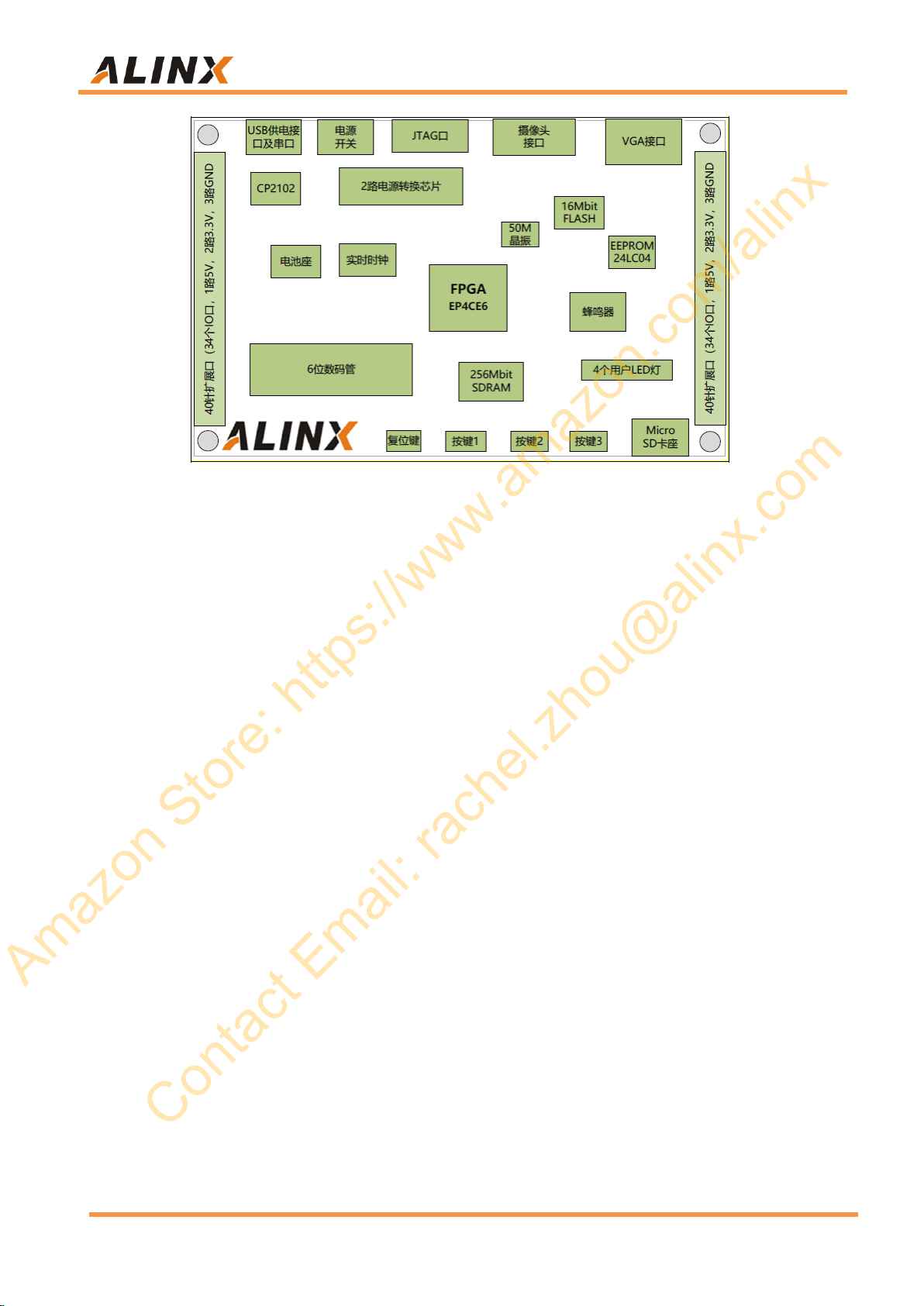
Part 1: FPGA Development Board Introduction..........................................5
Part 2: Power Supply..................................................................................7
Part 3: FPGA ..............................................................................................8
Part 3.1: JTAG Interface......................................................................9
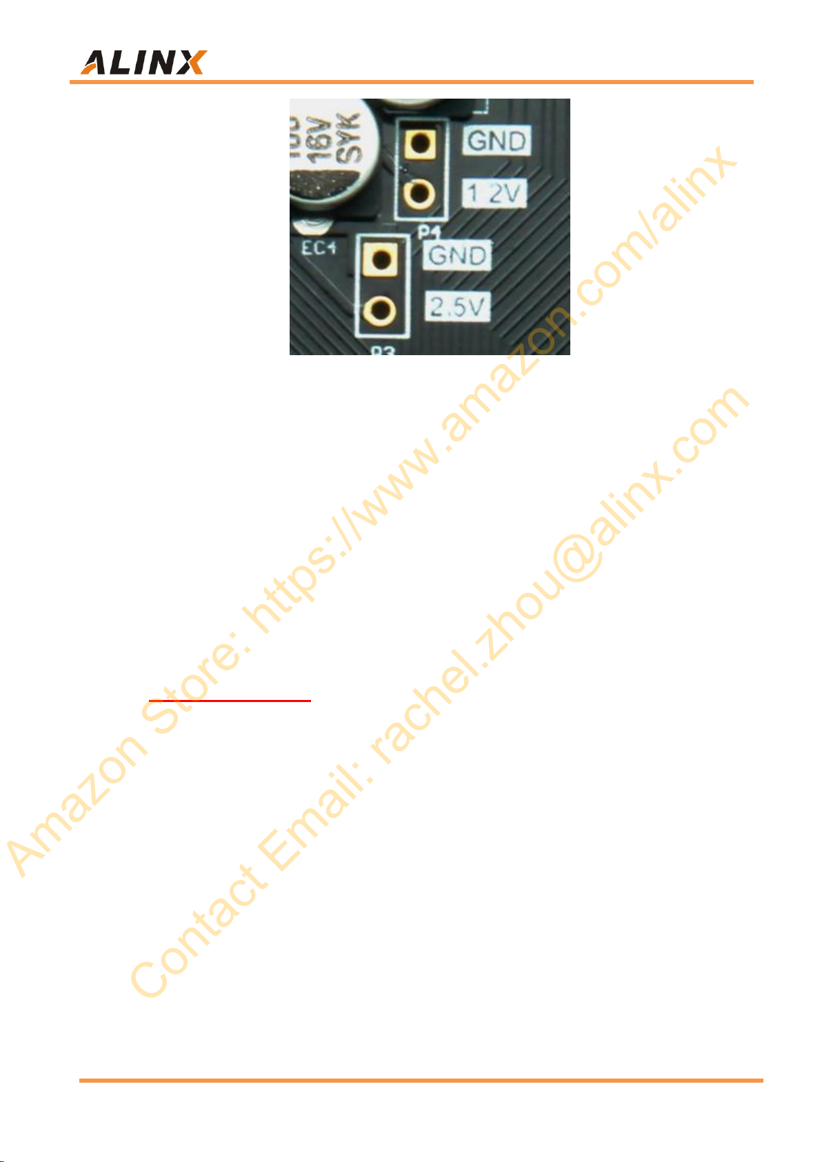
Part 3.2: FPGA power and GND pins................................................10
Part 4: 50M Active Crystal ........................................................................12
Part 5: SPI Flash ......................................................................................13
Part 6: SDRAM.........................................................................................14
Part 7: EEPROM 24LC04.........................................................................17
Part 8: Real-time clock DS1302 ...............................................................18
Part 9: USB to Serial Port.........................................................................19
Part 10: VGA Interface..............................................................................21
Part 11: SD Card Slot ...............................................................................24
Part 12: LEDs ...........................................................................................26
Part 13: User Keys ...................................................................................27
Part 14: Camera Module interface............................................................28
Part 15: Digital Tube.................................................................................29
Part 16: Buzzer.........................................................................................32
Part 17: Expansion Ports..........................................................................33

FPGA Development Board AX301 User Manual
4 / 36
Amazon Store: https://www.amazon.com/alinx
The ALINX AX301 development board is an entry-level product for
ALTERA FPGAs and is primarily targeted at FPGA beginners. AX301 uses
ALTERA's Cyclone IV series chip, the model is EP4CE6F17C8, and it is a
256-pin FBGA package. The configuration of the entire development board is
practical. There are two ALINX standard 40-pin 2.54 pitch expansion ports, a
total of 34 * 2 = 68 IOs. In addition, 5V power, 3.3V power, and multiple GNDs
are also available. It is a very good choice for DIY players. In addition, many
ALINX supporting modules can also be directly connected to the expansion
port of this FPGA development board, such as ADDA module, 4.3 inch LCD
screen, audio module, camera, etc. provide more options. The following is a
detailed introduction to AX301.

FPGA Development Board AX301 User Manual
5 / 36
Amazon Store: https://www.amazon.com/alinx
Part 1: FPGA Development Board Introduction
The AX301 development board uses ALTERA's Cyclone IV series FPGA,
the model is EP4CE6F17C8, and a 256-pin FBGA package. The resources of
this FPGA are shown below:
The main parameters as below:
Parameters
Value
Logic elements(LEs)
6272
Embedded memory(Kbits)
270
Embedded 18x18multipliers
15
Global Phase Locked Loop (PLLs)
2
Global Clock Networks
10
Maximum number of available IOs
179
Core voltage
1.15V-1.25V(recommend 1.2V);
Operating temperature
0-85℃
The structure of the entire system is shown in Figure 1-1:

FPGA Development Board AX301 User Manual
6 / 36
Amazon Store: https://www.amazon.com/alinx
Through the diagram, we can see the functions that the development
platform can achieve:
USB interface power supply, and realize USB to serial port function
A large-capacity 256Mbit SDRAM can be used as data cache
A 16Mbit SPI FLASH can be used as FPGA configuration file and user
data storage
One camera interface for 5 million OV5640 camera module
One VGA interface, VGA interface is 16bit, can display 65536 colors,
can display color pictures and other information
One piece of RTC real-time clock, equipped with a battery holder, the
battery model is CR1220
One EEPROM 24LC04 with IIC interface
4 red LEDs, can realize the function of running light
4 buttons, 1 reset button, 3 user button
50M active crystal on board, providing stable clock source for
development board
Two 40-pin ALINX standard expansion ports (2.54mm pitch), of which 34
IO ports, one 5V power supply, two 3.3V power supplies, and three
GND. Two expansion modules can be connected at the same time,

FPGA Development Board AX301 User Manual
7 / 36
Amazon Store: https://www.amazon.com/alinx
such as 4.3-inch TFT module and AD / DA module
The JTAG port is reserved for debugging and program curing of the
FPGA.
1 Micro SD card slot, support SPI mode One 6-digit digital tube, can
display 6 digits dynamically
Part 2: Power Supply
The AX301 development board is powered by USB. Use a MINI USB
cable to connect the development board to the computer's USB and press the
power switch to power the development board. The power supply design
diagram of the development board is as Figure 2-1:
Figure 2-1: Power Supply Schematic
The development board is powered by USB and generates three power
sources: + 3.3V, + 2.5V, and + 1.2V through three LDO power chips to meet the
bank voltage and core voltage of the FPGA.
In the PCB design, a 4-layer PCB is used, and a separate power supply
layer and GND layer are reserved, so that the power supply of the entire
development board has very good stability. Test points for each power supply
are reserved on the PCB so that the user can confirm the voltage on the board.

FPGA Development Board AX301 User Manual
8 / 36
Amazon Store: https://www.amazon.com/alinx
Figure 2-2: Test Points for Power supply on the Board
Part 3: FPGA
The FPGA model used by the AX301 development board is
EP4CE6F17C8, which belongs to ALTERA's Cyclone IV. This model is a BGA
package with 256 pins. The definition of FPGA pins is explained again. Many
people use FPGAs that are non-BGA packages, such as 144-pin, 208-pin
FPGA chips. Their pin definitions are composed of numbers, such as 1 to 144,
1 to 208, and so on. When we use a BGA packaged chip, the pin names
become letters + numbers, such as E3, G3, etc. Therefore, when reading the
schematic diagram, the letters + numbers in this form represent the FPGA Pin.
Having said this, let's look at the functions of various parts related to FPGA.
Figure 3-1 is the FPGA chip used in the development board.

FPGA Development Board AX301 User Manual
9 / 36
Amazon Store: https://www.amazon.com/alinx
Figure 3-1: The FPGA chip on the Board
Part 3.1: JTAG Interface
First of all, let's talk about the configuration and debugging interface of
FPGA: JTAG interface. The function of the JTAG interface is to download the
compiled program (.sof) into the FPGA or the FLASH configuration program
(.jic) to the SPI FLASH. After the sof file is downloaded to the FPGA, it will be
lost after power failure. You need to power on and download again. At this time,
we can convert the sof file into a jic file through the Quartus software. After
downloading the jic file to the development board's FLASH through JTAG, it will
not be lost after power off, and the FPGA will read the jic configuration file in
FLASH and run after power on again.
Figure 3-2 is the schematic part of the JTAG port, which involves the four
signals TCK, TDO, TMS, TDI. These four signals are directly derived from the
FPGA pins, and each signal has a diode overvoltage protection circuit on the

FPGA Development Board AX301 User Manual
10 / 36
Amazon Store: https://www.amazon.com/alinx
development board.
Figure 3-2: The JTAG port schematic
The JTAG interface uses a 10-pin 2.54mm standard connector. Figure 3-3
is the JTAG interface on the development board.
Figure 3-3: The JTAG port on the FPGA Board
Part 3.2: FPGA power and GND pins
Next, let's talk about the power pins of the FPGA. It includes the power
supply pin, core voltage pin, analog voltage and phase-locked loop power
supply pin of each bank. VCCINT is the FPGA core power supply pin, which is
connected to 1.2V. VCCIO is the power supply voltage of each bank of the

FPGA Development Board AX301 User Manual
11 / 36
Amazon Store: https://www.amazon.com/alinx
FPGA. Among them, VCCIO0 is the power supply pin of FPGA BANK0.
Similarly, VCCIO1 ~ VCCIO3 are the power supply pins of FPGA BANK ~
BANK3 respectively. In the development board, VCCIO is connected to 3.3V
voltage. Both pins are 3.3V input and output. VCCA is the FPGA analog power
supply pin, which is connected to 2.5V, VCCD_PLL is the FPGA phase-locked
loop power supply pin, and also connected to 1.2V. The power connection
diagram of the FPGA chip is shown in Figure 3-4.
Figure 3-4: FPGA power pins
In addition, there are many pins on the FPGA that need to be connected to
GND to ensure a stable ground reference inside the FPGA. The GND
connected to the FPGA is shown in Figure 3-5

FPGA Development Board AX301 User Manual
12 / 36
Amazon Store: https://www.amazon.com/alinx
Figure 3-5: FPGA GND Pin
Part 4: 50M Active Crystal
Figure 4-1 is a 50M active crystal circuit that provides a clock source for
the development board. Crystal output is connected to FPGA global input clock
pin (CLK1 pin E1). This CLK1 can be used to drive the user logic circuit in the
FPGA. The user can configure the FPGA's internal PLL (Phase Locked Loop)
to divide and multiply to achieve clocks of other frequencies.
Figure 4-1: 50M Active Crystal Circuit
Figure 4-2: 50M Active Crystal on the FPGA Board

FPGA Development Board AX301 User Manual
13 / 36
Amazon Store: https://www.amazon.com/alinx
Clock pin assignment:
Pin Name
FPGA Pin
CLK
E1
Part 5: SPI Flash
The AX301 FPGA development board is equipped with a 16Mbit SPI
FLASH chip, model W25P16, which uses the 3.3V CMOS voltage standard
and completely replaces the configuration chip EPCS16 of ALTERA. Due to its
non-volatile characteristics, in use, SPI FLASH can be used as the boot image
of the FPGA system. These images mainly include the JIC configuration files
for the FPGA, soft application code, and other user data files.
The specific model and related parameters of SPI FLASH are shown in
Table 5-1.
Position
Model
Capacity
Factory
U8
W25P16
16M Byte
ST
Table 5-1: SPI FLASH Specification
The SPI Flash schematic is shown in Figure 5-2
Figure 5-1: SPI Flash Connection Diagram

FPGA Development Board AX301 User Manual
14 / 36
Amazon Store: https://www.amazon.com/alinx
Figure 5-2: SPI Flash on the FPGA Board
Configure chip pin assignments:
Pin Name
FPGA Pin
DCLK
H1
nCSO
D2
DATA0
H2
ASDO
C1
Part 6: SDRAM
The AX301 FPGA development board has an SDRAM chip on board,
model: HY57V2562GTR, capacity: 256Mbit (16M * 16bit), 16bit bus. SDRAM
can be used for data buffering. For example, the data collected by the camera
is temporarily stored in SDRAM and then displayed through the VGA interface.
Here SDRAM is used for data caching.
The hardware connection of SDRAM is shown in Figure 6-1

FPGA Development Board AX301 User Manual
15 / 36
Amazon Store: https://www.amazon.com/alinx
Figure 6-1: SDRAM schematic
Figure 6-2: SDRAM on the FPGA Board

FPGA Development Board AX301 User Manual
16 / 36
Amazon Store: https://www.amazon.com/alinx
SDRAM pin assignment:
Pin Name
FPGA Pin
S_CLK
B14
S_CKE
F16
S_NCS
K10
S_NWE
J13
S_NCAS
J12
S_NRAS
K11
S_DQM<0>
J14
S_DQM<1>
G15
S_BA<0>
G11
S_BA<1>
F13
S_A<0>
F11
S_A<1>
E11
S_A<2>
D14
S_A<3>
C14
S_A<4>
A14
S_A<5>
A15
S_A<6>
B16
S_A<7>
C15
S_A<8>
C16
S_A<9>
D15
S_A<10>
F14
S_A<11>
D16
S_A<12>
F15
S_DB<0>
P14
S_DB<1>
M12
S_DB<2>
N14
S_DB<3>
L12
S_DB<4>
L13
S_DB<5>
L14
S_DB<6>
L11
S_DB<7>
K12
S_DB<8>
G16

FPGA Development Board AX301 User Manual
17 / 36
Amazon Store: https://www.amazon.com/alinx
S_DB<9>
J11
S_DB<10>
J16
S_DB<11>
J15
S_DB<12>
K16
S_DB<13>
K15
S_DB<14>
L16
S_DB<15>
L15
Part 7: EEPROM 24LC04
AX301 FPGA development board contains an EEPROM, model 24LC04,
and has a capacity of 4Kbit (2*256*8bit). It consists of two 256-byte blocks and
communicates via the IIC bus. The EEPROM is generally used in the design of
instruments and meters, and is used to store some parameters. This kind of
chip is easy to operate and has a very high price-performance ratio, so
although the capacity ratio is high, the price is very cheap. It is a good choice
for those products that require high cost. Figure 7-1 is the schematic diagram
of EEPROM
Figure 7-1: EEPROM Schematic

FPGA Development Board AX301 User Manual
18 / 36
Amazon Store: https://www.amazon.com/alinx
Figure 7-2: EEPROM on the FPGA Board
EEPROM Pin Assignment
Pin Name
FPGA Pin
SDA
E6
SCL
D1
Part 8: Real-time clock DS1302
The AX301 FPGA development board contains a real-time clock RTC chip,
model DS1302, which provides a calendar function up to 2099, with days,
minutes, minutes, seconds and weeks. If time is needed in the system, then the
RTC needs to be involved in the product. It needs to connect a 32.768KHz
passive clock to provide an accurate clock source to the clock chip, so that the
RTC can accurately provide clock information to the product. At the same time,
in order to power off the product, the real-time clock can still operate normally.
Generally, a battery is required to supply power to the clock chip. In Figure 8-1,
the U10 is the battery holder, and the button battery (model CR1220, voltage is
3V) is placed. After the system is turned off, the button battery can also supply
power to the DS1302. This way, regardless of whether the product is powered
or not, the DS1302 will operate normally without interruption and provide

FPGA Development Board AX301 User Manual
19 / 36
Amazon Store: https://www.amazon.com/alinx
continuous time information. Figure 8-1 shows the design of the DS1302:
Figure 8-1: DS1302 schematic
Figure 8-12: DS1302 on the FPGA Board
DS1302 interface pin assignment:
Pin Name
FPGA Pin
RTC_SClK
P6
RTC_nRST
N8
RTC_DATA
M8
Part 9: USB to Serial Port
The development board contains the Silicon Labs CP2102GM USB-UAR

FPGA Development Board AX301 User Manual
20 / 36
Amazon Store: https://www.amazon.com/alinx
chip. The USB interface uses the MINI USB interface. This USB interface
implements the power supply function, and it can implement the USB to serial
port function. You can use a USB cable to connect it to the USB port of the PC
for serial data communication.
The schematic diagram of the serial port is shown in Figure 9-1
Figure 9-1: USB to serial port schematic
Figure 9-2: USB to serial port on the FPGA Board
Other manuals for AX301
1
Table of contents
Other Alinx Motherboard manuals

Alinx
Alinx ARTIX-7FPGA User manual

Alinx
Alinx AXKU041 User manual

Alinx
Alinx ZYNQ7000 FPGA User manual

Alinx
Alinx AXU4EVB-E User manual

Alinx
Alinx ZYNQ7000 FPGA User manual

Alinx
Alinx AV4040 User manual

Alinx
Alinx ACU3EG User manual

Alinx
Alinx Zynq UltraScale+MPSoC User manual

Alinx
Alinx ZYNQ7000 FPGA User manual

Alinx
Alinx AX7202 User manual

Alinx
Alinx AX7102 User manual

Alinx
Alinx AV4075 User manual

Alinx
Alinx ZYNQ UltraScale+ User manual

Alinx
Alinx ARTIX-7 FPGA User manual

Alinx
Alinx ARTIX-7FPGA User manual

Alinx
Alinx AXKU040 User manual

Alinx
Alinx KINTEX-7 FPGA User manual

Alinx
Alinx ZYNQ7000 FPGA User manual

Alinx
Alinx AC7Z100 User manual

Alinx
Alinx ACU15EG User manual