Alinx AV4075 User manual

FPGA Video Processing
Development Platform
AV4075
User Manual

FPGA Video Processing Development Platform AV4075 User Manual
2 / 56
Amazon Store: https://www.amazon.com/alinx
Version Record
Version
Date
Release By
Description
Rev 1.0
2019-05-01
Rachel Zhou
First Release

FPGA Video Processing Development Platform AV4075 User Manual
3 / 56
Amazon Store: https://www.amazon.com/alinx
Table of Contents
Version Record.......................................................................................... 2
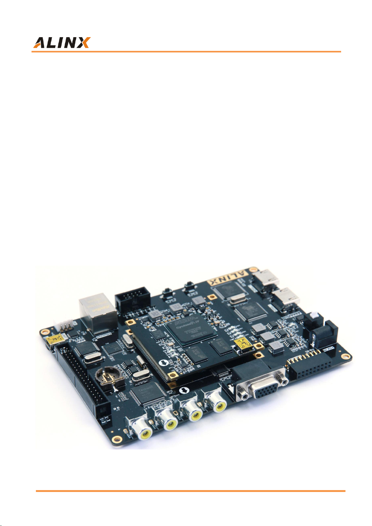
Part 1: FPGA Development Board Introduction......................................... 6
Part 2: Function realization........................................................................ 8
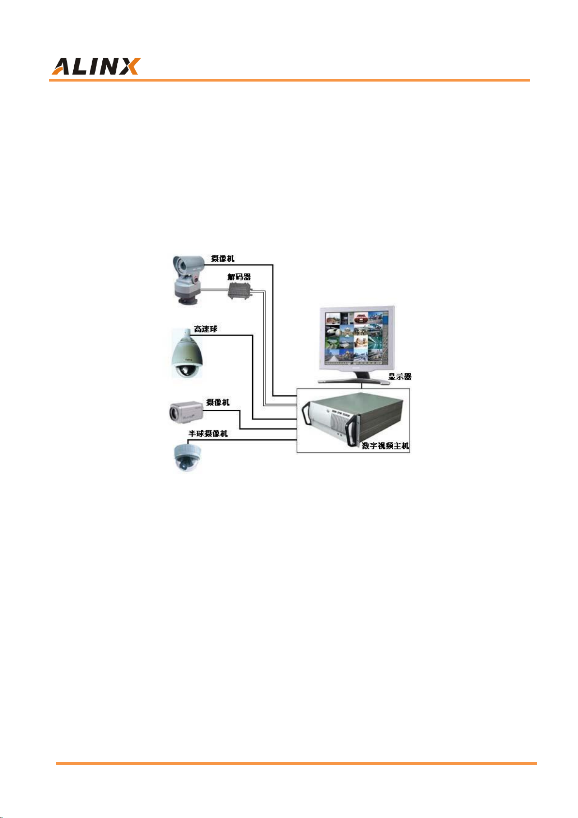
Part 2.1: Video Input............................................................................8
Part 2.2: Video Output.......................................................................11
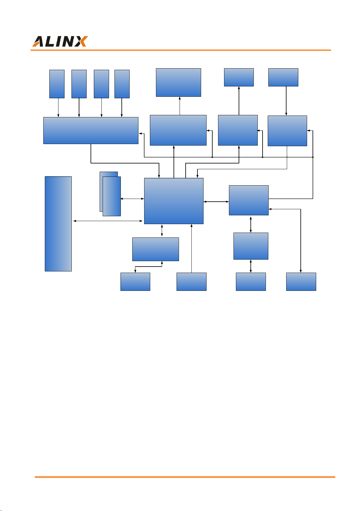
Part 3: AC4075 core board...................................................................... 12
Part 3.1: AC4075 Core Board Introduction........................................13
Part 3.2: DDR2 DRAM ......................................................................13
Part 3.3: SPI Flash ............................................................................16
Part 3.4: FPGA Power Supply...........................................................17
Part 3.5: Expansion Ports..................................................................19
Part 3.6: Powe interface on Core Board............................................22
Part 3.7: Crystal oscillator on Core Board .........................................23
Part 3.8: LED Light on Core Board....................................................25
Part 3.9: Structure Diagram...............................................................28
Part 4: Carrier Board ................................................................................29
Part 4.1: Carrier Board Introduction ..................................................29
Part 4.2: VGA Display Interface.........................................................30
Part 4.3: HDMI Output Interface........................................................33
Part 4.4: HDMI Input Interface...........................................................35
Part 4.5: Video input interface...........................................................37
Part 4.6: Gigabit Ethernet Interface...................................................39
Part 4.7: ARM Controller ...................................................................42
Part 4.8: Camera Module Interface ...................................................49
Part 4.9: Expansion Header ..............................................................50
Part 4.10: JTAG Interface..................................................................52

FPGA Video Processing Development Platform AV4075 User Manual
4 / 56
Amazon Store: https://www.amazon.com/alinx
Part 4.11: Buttons..............................................................................53
Part 4.12: Power Supply....................................................................54

FPGA Video Processing Development Platform AV4075 User Manual
5 / 56
Amazon Store: https://www.amazon.com/alinx
Professional ALTERA FPGA Video Processing development platform
(module: AV4075) adopts the core board + carrier board mode, which is
convenient for users to use the core board for secondary development.
This FPGA video image processing development platform is derived from
the improvement of our company's ALTERA video development board AX822.
In terms of hardware design, we added HDMI input, Gigabit Ethernet, CMOS
Camera interface and Micro in the original design. This greatly enriches the
functions of the video image processing board, not only satisfies the functions
of FPGA video image processing, but also provides network communication for
video image storage and video images. Therefore, this development platform
can be called "professional" and "all-round". Such a product is very suitable for
students, engineers and other groups engaged in FPGA video image
processing or video image communication and storage.

FPGA Video Processing Development Platform AV4075 User Manual
6 / 56
Amazon Store: https://www.amazon.com/alinx
Part 1: FPGA Development Board Introduction
The entire structure of the AV4075 FPGA development board is inherited
from our consistent core board + carrier board model. A high-speed inter-board
connector is used between the core board and the carrier board.
The core board is mainly composed of FPGA+ 2DDR2+ FLASH. It
undertakes the core algorithm of video image processing, fully utilizes the
parallel processing capability of FPGA, and the high-speed data reading and
writing between FPGA and DDR2. The bandwidth of the whole system is up to
8.5Gb/s (266.7M*32bit); In addition, DDR2 capacity is up to 2Gbit, which meets
the need for high buffers during video processing. The selected FPGA is the
high-speed FPGA chip of EP4CE75F23C8 of ALTERA CYCLONE IV series.
The FPGA is packaged in BGA484. The FPGA and two DDR2 chips are
connected to form a 32-bit bus width. The communication frequency between
FPGA and DDR2 is 133.3Mhz, and the internal frequency of DDR2 is
266.7Mhz. This high frequency and high bandwidth design fully meets the
needs of four 1080p video processing.

FPGA Video Processing Development Platform AV4075 User Manual
7 / 56
Amazon Store: https://www.amazon.com/alinx
ALTERA
EP4CE75F23
C8
ARM
DDR2
TW2867
视频
输入
接口
视频
输入
接口
视频
输入
接口
视频
输入
接口
ADV7123
VGA输出
SiI9134
HDMI输出
SiI9013
HDMI输入
RTL8211E
以太网网
口CMOS接口
CP2102
USB UART SD Card
40PIN Connector
DDR2
Figure 1-1-1: The Schematic Diagram of the AV4075
Through this diagram, you can see the interfaces and functions that the
AV4075 FPGA Development Board contains:
4-channel video input
Select Techwell TW2867, can input 4 composite video signals,
PAL/NTSC/SECAM automatic identification, output BT656,
multiplexable bus, FPGA-side demultiplexing, saving IO
1-channel VGA Output
The ADV7123, a three-channel, 10-bit DAC converter from Analog
Devices, supports RGB digital input and VGA output. Supports

FPGA Video Processing Development Platform AV4075 User Manual
8 / 56
Amazon Store: https://www.amazon.com/alinx
conversion rates up to 240MSPS, up to 1080p@60Hz video image
output
1-channel HDMI Output
Select Silion Image SIL9134 HDMI encoding chip, support up to
1080P@60Hz output, support 3D output.
1-channel HDMI Input
Select Silion Image SIL9013 HDMI decoder chip, support up to
1080P@60Hz input, support different formats of data output
1-channel 10/100M/1000M Ethernet with RJ-45 interface
The Gigabit Ethernet interface chip uses Realtek's RTL8211EG
Ethernet PHY chip to provide network communication services to users.
The RTL8211EG chip supports 10/100/1000 Mbps network
transmission rate;
1-channel CMOS Input
CMOS camera interface, can be connected to ALINX 5 megapixel
OV5640 camera module
On the FPGA carrier board, an ARM chip (STM32F103) is mounted on the
board, and each interface chip and FPGA on the board are configured through
I2C.
Part 2: Function realization
Part 2.1: Video Input
The video development board can input 4 composite video signals through
TW2867, PAL/NTSC/SECAM automatically recognizes and output BT656; or
through SIL9013, can input HDMI video signals; or through CMOS interface,
can input image signals acquired by CMOS camera. Therefore, there are many

FPGA Video Processing Development Platform AV4075 User Manual
9 / 56
Amazon Store: https://www.amazon.com/alinx
video sources available for development boards, such as:
1)Surveillance cameras
Through the FPGA development board, it is possible to realize
four-channel surveillance camera through the display (VGA/DVI/HDMI
interface, which can realize 1080p) for split-screen display. Our development
board is equivalent to the digital video host in the Figure below.
Figure 2-1-1: Split Screen Display Surveillance cameras
2)Set top box
The video source obtained by connecting the HDMI output of the set-top
box can be used to implement picture-in-picture (PIP) function through FPGA
development platform.

FPGA Video Processing Development Platform AV4075 User Manual
10 / 56
Amazon Store: https://www.amazon.com/alinx
Figure 2-1-2: Set top box
3)Camera Module
CMOS camera interface, plug in ALINX 30 megapixel camera module or 5
megapixel camera module, real-time display 1080P video image on VGA
display or HDMI display.
Figure 2-1-3: 5 megapixel camera module AN5640

FPGA Video Processing Development Platform AV4075 User Manual
11 / 56
Amazon Store: https://www.amazon.com/alinx
Part 2.2: Video Output
There are two kinds of video output on the FPGA development board: you
can connect a VGA monitor to display VGA images; you can also connect
HMDI monitors or TV to display HDMI video signals. The video display for VGA
and HDMI output is up to 1080P@60Hz.
Current computer monitors basically support one of VGA or HDMI inputs.
As long as one of the VGA/HDMI interfaces of the display is connected to the
FPGA development board, the effect demonstration of the video image can be
realized. The picture below shows a computer monitor with VGA and HDMI
display connectors.
Figure 2-2-1: VGA/HDMI interfaces of the computer monitor

FPGA Video Processing Development Platform AV4075 User Manual
12 / 56
Amazon Store: https://www.amazon.com/alinx
Part 3: AC4075 core board

FPGA Video Processing Development Platform AV4075 User Manual
13 / 56
Amazon Store: https://www.amazon.com/alinx
Part 3.1: AC4075 Core Board Introduction
FPGA+ 2DDR2 core board is based on ALTERA CYCLONE IV series
EP4CE75F23C8. This chip develops a high-performance core board with high
speed, high bandwidth and high capacity. It is suitable for video image
processing and high-speed data acquisition.
This core board uses two pieces of MICRON's MT47H64M16HR-3IT
DDR2 chip with a total capacity of 2Gbit; two DDR2s form a 32-bit bus mode,
and the read/write data bandwidth between FPGA and DDR2 is up to 8.5Gb;
this configuration can satisfy 4 channels of 1080p video processing needs.
This core board extends 168 IO ports (73 pairs of LVDS differential), which
is a good choice for users who need a lot of IO. Moreover, the FPGA chip to the
interface is treated with the same length, and the core board size is only 60*60
(mm), which is very suitable for secondary development.
Part 3.2: DDR2 DRAM
Figure 3-2-1 detailed part of the DDR2 schematic (For details, please refer
to the schematic provided by us.)
Figure 3-2-1: DDR2 schematic

FPGA Video Processing Development Platform AV4075 User Manual
14 / 56
Amazon Store: https://www.amazon.com/alinx
Further, in order to allow DDR2 work properly, it is necessary to provide a
reference voltage VREF and the termination voltage VTT is DDR2 DDR2 chip
address lines and control lines, and VTT voltage VREF are 0.9V. Figure 3-2-1
detailed the power supply schematic below:
Figure 3-2-2: DDR2 Power for VTT/VREF
Figure 3-2-3: DDR2 Power Circuit on the Core Board
DDR2 connected to the BANK3 and BANK4 of the FPGA.
DDR2 Pin Assignment
Pin Name
FPGA Pin
Pin Name
FPGA Pin
DDR2_A[0]
R14
DDR2_A[11]
AA3

FPGA Video Processing Development Platform AV4075 User Manual
15 / 56
Amazon Store: https://www.amazon.com/alinx
DDR2_A[1]
AB5
DDR2_A[12]
AA20
DDR2_A[2]
T16
DDR2_BA[0]
AA6
DDR2_A[3]
U17
DDR2_BA[1]
R16
DDR2_A[4]
AA4
DDR2_BA[2]
AB10
DDR2_A[5]
U15
DDR2_nCAS
Y17
DDR2_A[6]
Y4
DDR2_CKE
AA8
DDR2_A[7]
AA19
DDR2_CLK_P
Y14
DDR2_A[8]
AB3
DDR2_CLK_N
Y15
DDR2_A[9]
U16
DDR2_DQ[16]
AB18
DDR2_A[10]
Y6
DDR2_DQ[17]
W15
DDR2_nRAS
U14
DDR2_DQ[18]
W17
DDR2_nWE
AB6
DDR2_DQ[19]
AB16
DDR2_ODT
AA17
DDR2_DQ[20]
V14
DDR2_DM[0]
AA7
DDR2_DQ[21]
AB20
DDR2_DM[1]
V5
DDR2_DQ[22]
V15
DDR2_DM[2]
AA16
DDR2_DQ[23]
T15
DDR2_DM[3]
A10
DDR2_DQ[24]
AA15
DDR2_DQ[0]
Y10
DDR2_DQ[25]
AA13
DDR2_DQ[1]
AB7
DDR2_DQ[26]
AB15
DDR2_DQ[2]
AA9
DDR2_DQ[27]
AA14
DDR2_DQ[3]
AB8
DDR2_DQ[28]
AB13
DDR2_DQ[4]
U10
DDR2_DQ[29]
U12
DDR2_DQ[5]
V11
DDR2_DQ[30]
AB14
DDR2_DQ[6]
Y8
DDR2_DQ[31]
W13
DDR2_DQ[7]
W10
DDR2_DQS[0]
AB9
DDR2_DQ[8]
V8
DDR2_DQS[1]
V10
DDR2_DQ[9]
AA5
DDR2_DQS[2]
V13
DDR2_DQ[10]
Y7
DDR2_DQS[3]
Y13
DDR2_DQ[11]
W7
DDR2_DQ[12]
W6
DDR2_DQ[13]
U9
DDR2_DQ[14]
Y3
DDR2_DQ[15]
W8

FPGA Video Processing Development Platform AV4075 User Manual
16 / 56
Amazon Store: https://www.amazon.com/alinx
Part 3.3: SPI Flash
The AC4075 FPGA core board is equipped with one 64MBit SPI FLASH,
and the model is M25P64, which uses the 3.3V CMOS voltage standard. Due
to the non-volatile nature of SPI FLASH, it can be used as a boot device for the
system to store the boot image of the system. These images mainly include
FPGA bit files, core application code and other user data files. The specific
models and related parameters of SPI FLASH are shown in Table 3-3-1.
Position
Model
Capacity
Factory
U8
M25P64
64M Bit
ST
Table 3-3-1: SPI FLASH Specification
Figure 3-3-1: SPI Flash schematic
Figure 3-3-2: M25P64 chip on the FPGA Board

FPGA Video Processing Development Platform AV4075 User Manual
17 / 56
Amazon Store: https://www.amazon.com/alinx
SPI Flash pin assignments:
Pin Name
FPGA Pin
DCLK
K2
nCSO
E2
DATA0
K1
ASDO
D1
Part 3.4: FPGA Power Supply
In order for FGPA to work properly, we need to provide 3.3V, 1.8V, 2.5V,
1.2V and VCCIO five-way power for the FPGA. Let's talk about the power pin
portion of the FPGA, which includes the power pins for each bank, the core
voltage pins, the analog voltage, and the phase-locked loop power supply pins.
VCCINT is the FPGA core power supply pin, connected to 1.2V; VCCIO is
the power supply voltage of each BANK of the FPGA, where VCCIO1 is the
power supply pin of the BANK1 of the FPGA. Similarly, VCCIO2~VCCIO8 are
the power supply of the BANK2~BANK8 of the FPGA respectively. In the
AC4040 core board, VCCIO3 and VCCIO4 are connected to 1.8V, because
BANK3 and BANK4 are IOs connected to DDR2. The other BANK (BANK1~2,
BANK5~8) voltages are connected to the adjustable VCCIO, which enables the
BANK IO voltage of the FPGA to be flexibly adjusted. By adjusting the
resistance value of the VCCIO power supply part, different output voltages are
obtained, so that the FPGA core The board's IO level can be applied to different
voltages (the default VCCIO voltage is 3.3V). In addition, with DDR2 on the
core board, a termination power supply VTT and a reference power supply
VREF for DDR2 are required.
The power supply (VCCIO, 1.2V, 1.8V) with three large current
requirements on the FPGA development board adopts the TLV62130RGT
DCDC chip imported from TI Company of the United States. It has high

FPGA Video Processing Development Platform AV4075 User Manual
18 / 56
Amazon Store: https://www.amazon.com/alinx
efficiency, small size, no heat, can provide large current, small ripple, etc. It is
an excellent power solution for FPGA; a large number of high-grade imported
capacitors are used to ensure the system's power supply is stable and reliable.
The three-way DCDC power supply circuit is designed as follows:
Figure 3-4-1: DC-DC Power Supply Schematic

FPGA Video Processing Development Platform AV4075 User Manual
19 / 56
Amazon Store: https://www.amazon.com/alinx
The other two channels (3.3V and 2.5V) use less LDO chips
SPX3819M5-L-3-3 and SPX3819M5-L-2-5 because of the low current required.
Figure 3-4-2: LDO Power Supply Schematic
Figure 3-4-3: Power Supply Circuit on the Core Board
Part 3.5: Expansion Ports
The core board has a total of two high-speed expansion ports, which is
connected with the FPGA carrier board by two 100-pin inter-board connectors.
The inter-board connector uses AMP Tyco board-to-board connector
5177984-4, with a PIN pitch of 0.8mm, and a male connector with a height of
5mm. It is connected with the female AMP connector 5177983-4 of the FPGA

FPGA Video Processing Development Platform AV4075 User Manual
20 / 56
Amazon Store: https://www.amazon.com/alinx
carrier board, which is configured for high speed data communication.
Figure 3-5-1: Expansion Ports P1
Table of contents
Other Alinx Motherboard manuals

Alinx
Alinx ZYNQ7000 FPGA User manual

Alinx
Alinx AC7Z035B User manual

Alinx
Alinx ARTIX-7 FPGA User manual

Alinx
Alinx ZYNQ7000 FPGA User manual

Alinx
Alinx AX301 User manual

Alinx
Alinx ZYNQUltraScale+ AXU3EGB User manual

Alinx
Alinx AXKU040 User manual

Alinx
Alinx ACU15EG User manual

Alinx
Alinx AX7102 User manual

Alinx
Alinx AXU4EVB-E User manual

Alinx
Alinx ACU3EG User manual

Alinx
Alinx AXU2CGA User manual

Alinx
Alinx ZYNQ UltraScale+ User manual

Alinx
Alinx ZYNQ7000 FPGA User manual

Alinx
Alinx Cyclone IV FPGA User manual

Alinx
Alinx AV4040 User manual

Alinx
Alinx AX7202 User manual

Alinx
Alinx ZYNQ UltraScale+ AXU9EGB User manual

Alinx
Alinx Zynq UltraScale+MPSoC User manual

Alinx
Alinx ZYNQ7000 FPGA User manual