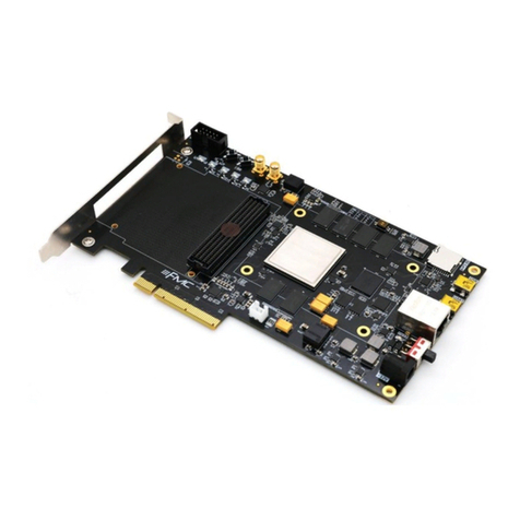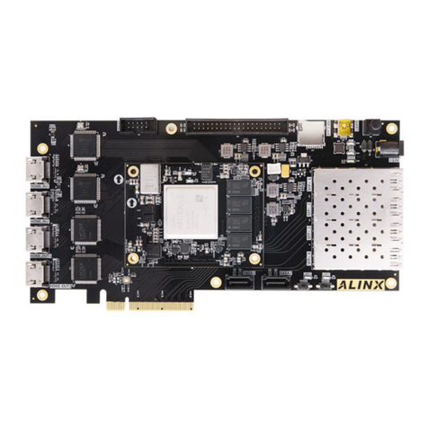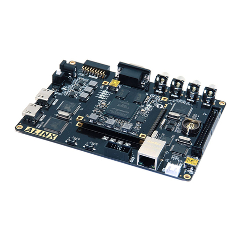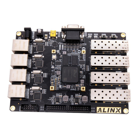
-External Memory Interface, Support 32/64bit DDR4/3/3L、LPDDR4/3 interface.
-Static storage interface, Support NAND, 2xQuad-SPI FLASH.
-High speed connection interface, SupportPCIe Gen2 x4, 2xUSB3.0, Sata 3.1,
DisplayPort, 4x Tri-mode Gigabit Ethernet.
-Ordinary connection interface:2xUSB2.0, 2x SD/SDIO, 2x UART, 2x CAN 2.0B, 2x
I2C, 2x SPI, 4x 32b GPIO.
-Power management: Support division of four power sources Full/Low/PL/Battery
-Encryption algorithm: Support RSA, AES & SHA.
-System monitor: 10 bit 1Mbps AD sampling for temperature and voltage
detection.
The main parameters of the PL logic part are as follows:
- System Logic Cells:1143K;
- CLB flip-flops): 1045K;
- CLBLUTs : 523K;
- Block RAM:34.6Mb;
- Clock Management Unit(CMTs): 11 pieces
- DSP Slices:1968 pieces
- GTH 16.3Gb/s Transceiver: 44 pieces
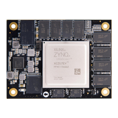
The speed level of XCZU19EG-2FFVC1760I chip is -2, industrial grade, and
packaged as FFVC1760.
Part 1.2 DDR4 DRAM
The ACU19EG core board is equipped with 9 Micron (Micron) 1GB DDR4 chips,
model MT40A1G16KD-062E, with 5 DDR4 chips mounted on the PS side, forming a 72
bit data bus bandwidth (supporting ECC), and each DDR chip has a capacity of 1GB.
Mount four DDR4 chips on the PL end to form a 64 bit data bus bandwidth, with each
DDR chip having a capacity of 1GB. The maximum operating speed of the DDR4
SDRAM on the PS side can reach 1200MHz (data rate 2400Mbps), and the four DDR4
storage systems are directly connected to the storage interface of the BANK504 on
the PS. The maximum operating speed of the DDR4 SDRAM on the PL side can reach
1200MHz (data rate 2400Mbps), and four DDR4 chips are connected to the
BANK69,70,71 interfaces of the FPGA. The specific configurations of DDR4 SDRAM on
the PS and PL ends are shown in Table 2-3-1.
