CONTENT
1.
OVER VIEW............................................................................................... 5
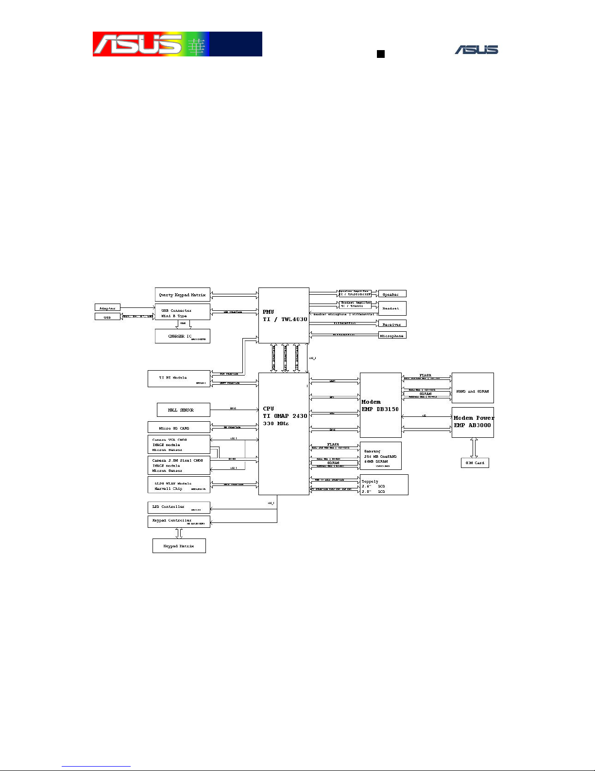
1.1
S
YSTEM BLOCK DIAGRAM
............................................................................ 5
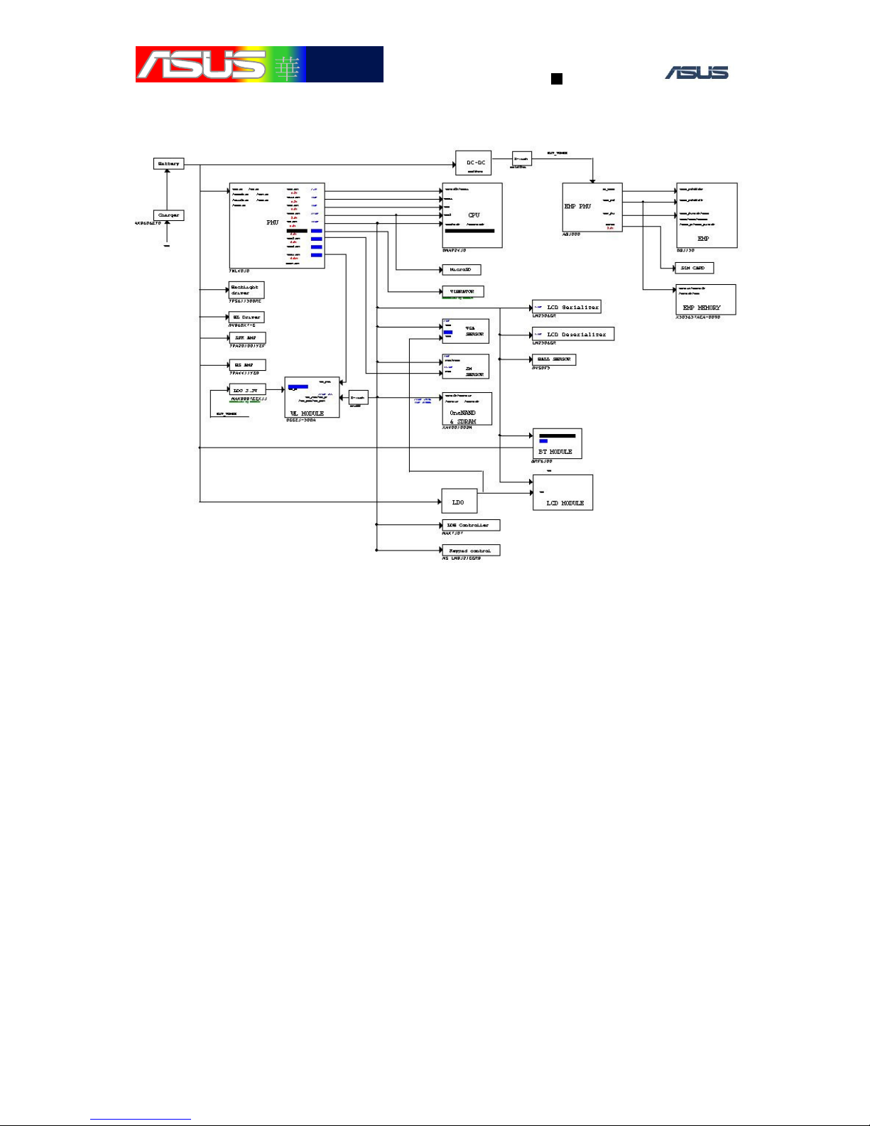
1.2
P
OWER
D
OMAIN
B
LOCK
.............................................................................. 6
1.3
P
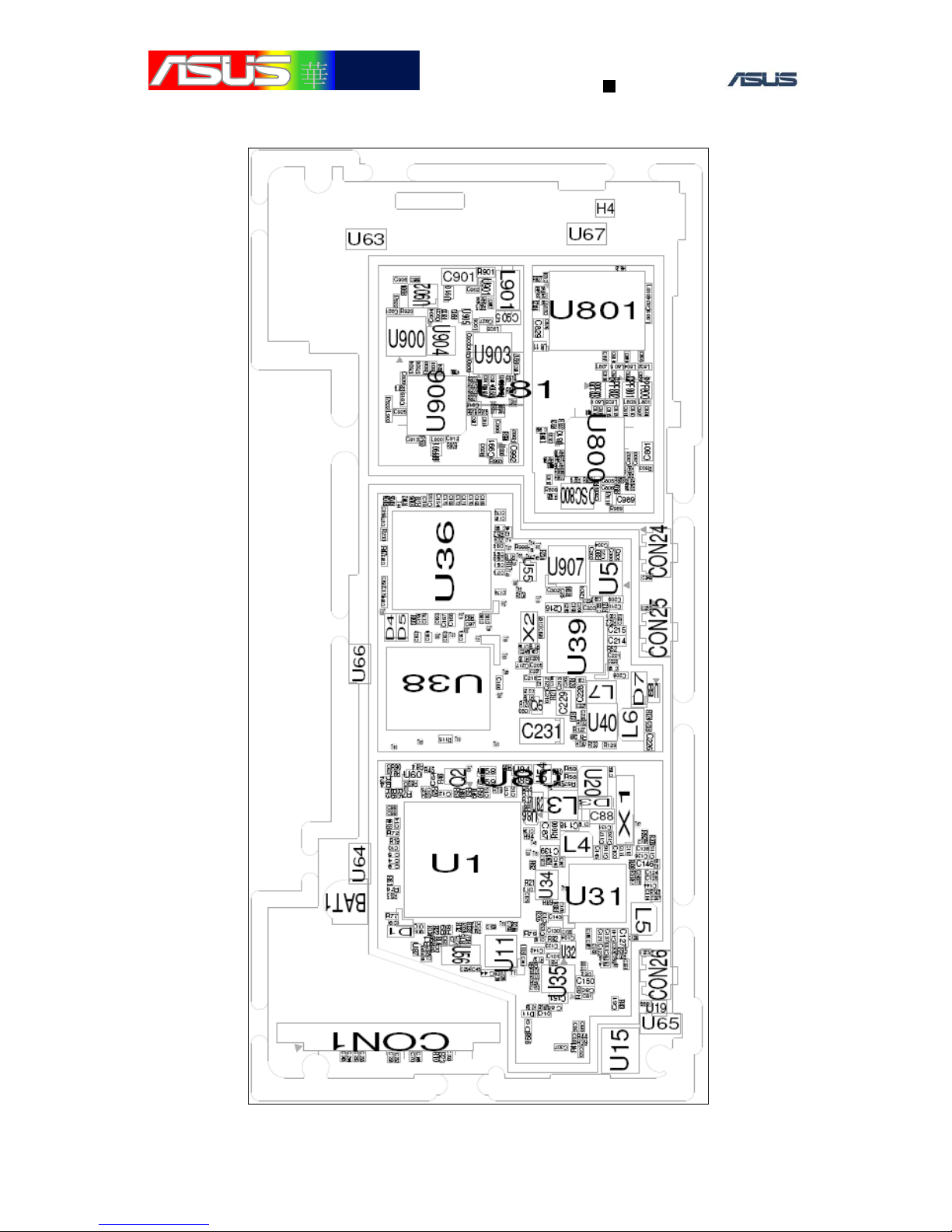
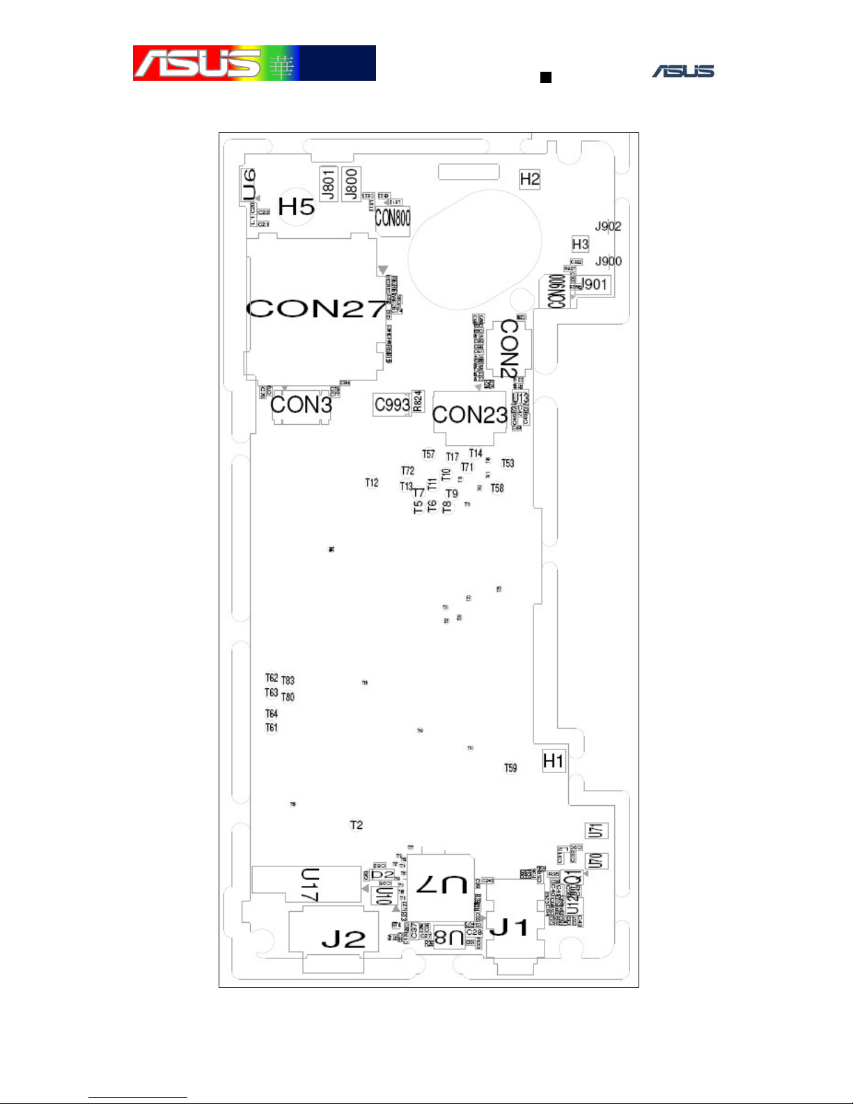
LACEMENT
TOP
V
IEW
............................................................................... 7
1.4
P
LACEMENT
B
OTTOM
V
IEW
......................................................................... 8
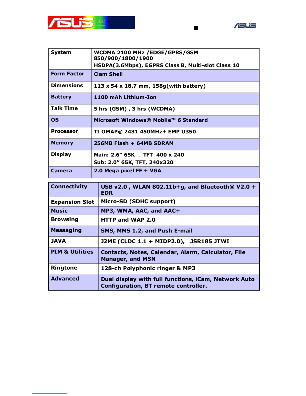
1.5
S
PECIFICATION
............................................................................................. 9
2.
SYSTEM CAN’T BOOT ......................................................................... 10
3.1
P
OWER
-
ON SEQUENCE
................................................................................ 10
1.2
O
THERS
...................................................................................................... 11
3.
MMI TEST ITEM .................................................................................... 13
4.1
M
ICRO
SD
T
EST
......................................................................................... 13
4.2
SIM
T
EST
.................................................................................................. 13
4.3
D
ISPLAY
T
EST
............................................................................................ 14
4.4
V
IBRATOR
T
EST
......................................................................................... 15
4.5
LED
T
EST
.................................................................................................. 15
2.5.1
RGB Led fail ..................................................................................... 15
2.5.2 Keypad LED fail ................................................................................ 15
4.6
2M
C
AMERA
&
VGA
C
AMERA
T
EST
......................................................... 16
4.7
SDRAM
&
F
LASH
T
EST
............................................................................ 17
4.8
A
UDIO
T
EST
............................................................................................... 18
4.8.1 Headset fail........................................................................................ 18
4.8.2 Speaker .............................................................................................. 19
4.8.3 On-Board Microphone can’t record ................................................. 20
4.8.4 Receiver ............................................................................................. 20
4.9
K
EYPAD
T
EST
............................................................................................ 21
4.9.1 Board level test:................................................................................. 21
4.9.2 External Keypad ................................................................................ 21
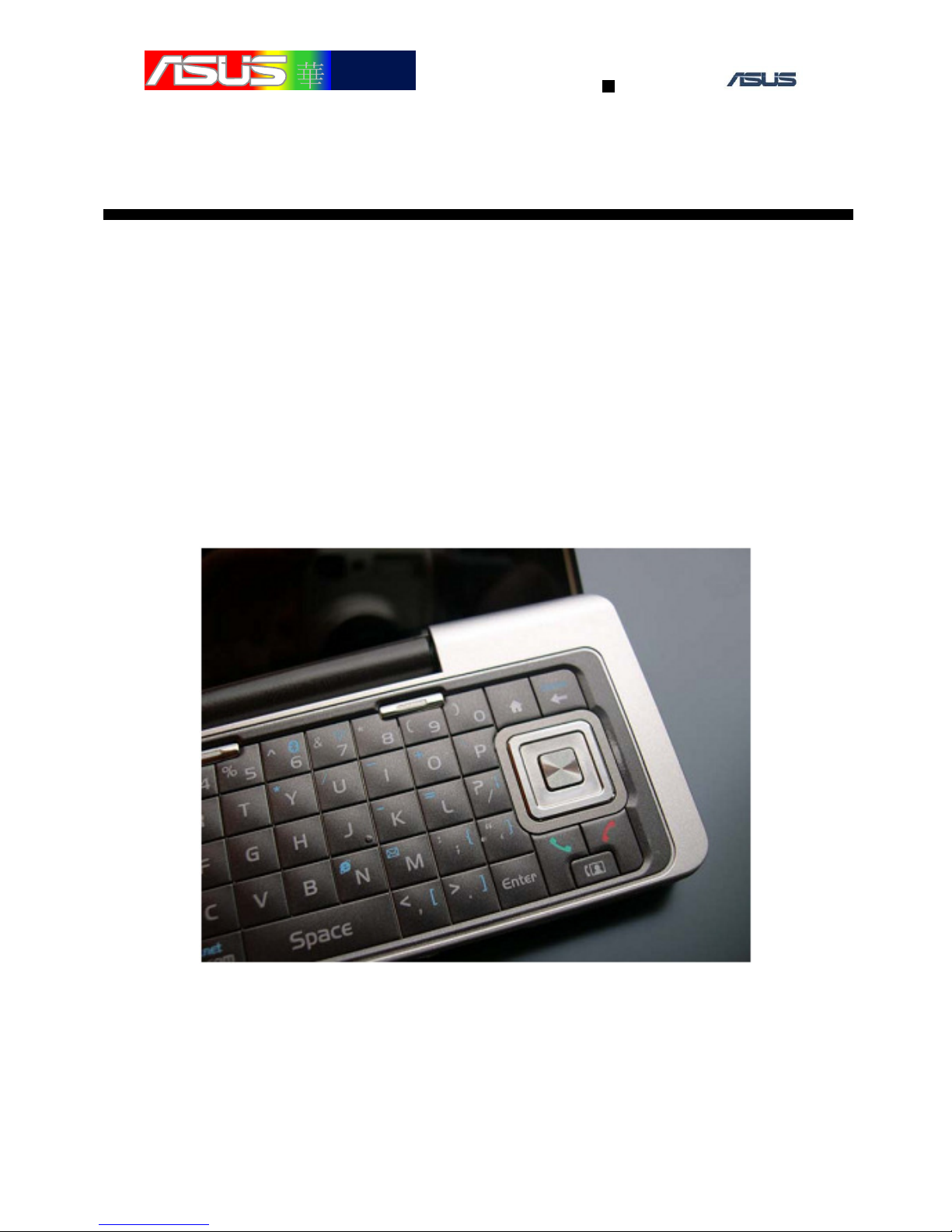
4.9.3 Internal Qwerty Keypad .................................................................... 22
4.10
BT
T
EST
.................................................................................................. 22
4.11
W
I
F
I
T
EST
............................................................................................... 23


 Operation and maintenance manual")