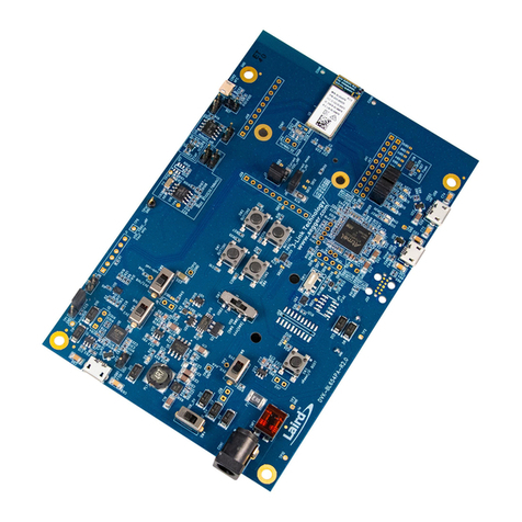
Avnet Xilinx Zynq 7Z045 User manual

Page 1
Copyright © 2017 Avnet, Inc. AVNET, “Reach Further,” and the AV logo are registered
trademarks of Avnet, Inc. All other brands are the property of their respective owners.
LIT# 5151-GSG-AES-7Z7045-G-01-V1
Xilinx®Zynq®7Z045
Mini-Module Plus
Development Kit
Version 1.0

Page 2
Document Control
Document Version: 1.0
Document Date: 8/28/2013
Revision History
Version
Date
Comment
1.0
8/28/2013
Initial release for production board (AES-MMP-7Z045-G Revision B)

Page 3
Avnet Design Kit Technical Support Files and Downloads
Web Access Instructions
Thank you for purchasing an Avnet design kit. The technical support documents associated with this kit,
including the User Guide, Bill of Materials, Schematics, Source Code and Application Notes, are available
online. You, the Customer, can access these documents at any time by visiting Avnet’s Design Resource
Center (“DRC”) at: avnet.com/us/drc
On your first visit to the DRC, You will be required to site register before you can download the documents. To
get started, select the name of the manufacturer associated with your design kit from the drop down menu. A
completelistingof availabledesign kitswill appear.Selectthekityoupurchased.Scrolltothe bottom ofthedesign
kit page to access the support files. Before you download a file, you will be prompted to login.If youareanexisting
user, please login. If you are a new user, click on the “Need to sign-up?” text. Please complete the short
registration form. Upon completion, be sure to retain your login and password information for future visits to
Avnet’s DRC. Logging in once gives you unlimited access to all technical support files and downloads. You will
also have the chance to request email notifications whenever there are updates to your design kit.
License Agreement
THE AVNET DESIGN KIT (“DESIGN KIT” OR “PRODUCT”) AND ANY SUPPORTING
DOCUMENTATION (“DOCUMENTATION” OR “PRODUCT DOCUMENTATION”) IS SUBJECT TO
THIS LICENSE AGREEMENT (“LICENSE”). USE OF THE PRODUCT OR DOCUMENTATION
SIGNIFIES ACCEPTANCE OF THE TERMS AND CONDITIONS OF THIS LICENSE. THE TERMS
OF THIS LICENSE AGREEMENT ARE IN ADDITION TO THE AVNET CUSTOMER TERMS AND
CONDITIONS, WHICH CAN BE VIEWED AT www.avnet.com. THE TERMS OF THIS LICENSE
AGREEMENT WILL CONTROL IN THE EVENT OF A CONFLICT.
1. Limited License. Avnet grants You, the Customer, (“You” “Your” or “Customer”) a limited, non-
exclusive, non-transferable, license to: (a) use the Product for Your own internal testing, evaluation
and design efforts at a single Customer site; (c) make, use and sell the Product in a single production
unit. No other rights are granted and Avnet and any other Product licensor reserves all rights not
specifically granted in this License Agreement. Except as expressly permitted in this License, neither
the Design Kit, Documentation, nor any portion may be reverse engineered, disassembled,
decompiled, sold, donated, shared, leased, assigned, sublicensed or otherwise transferred by
Customer. The term of this License is in effect until terminated. Customer may terminate this license
at any time by destroying the Product and all copies of the Product Documentation.
2. Changes. Avnetmay make changes to the Product or Product Documentation at anytimewithout notice.
Avnet makes no commitment to update orupgrade theProduct or Product Documentation andAvnet
reserves the right to discontinue the Product orProduct Documentation atany time without notice.
3. Product Documentation. Product Documentation is provided by Avnet on an “AS-IS” basis and does
not form a part of the properties of the Product. All Product Documentation is subject to change
without notice. Avnet makes no representation as to the accuracy or completeness of the Product
Documentation, and DISCLAIMS ALL REPRESENTATIONS, WARRANTIES AND LIABILITIES
UNDER ANY THEORY WITH RESPECT TO PRODUCT INFORMATION.
4. LimitedProductWarranty.AVNETWARRANTSTHATATTHETIMEOFDELIVERY,THEPRODUCTSSHALL
MEETTHESPECIFICATIONSSTATEDINAVNETDOCUMENTATIONFORSIXTY(60)DAYSFROM
DELIVERYOFPRODUCTS.IFTHECUSTOMERCANPROVIDEPROOFTHATTHEQUALIFIEDAVNET
PRODUCTWASPURCHASEDFORTHEPURPOSEOFANDDEPLOYEDASACOMPONENTINTHE
CUSTOMER’S COMMERCIALLY AVAILABLE PRODUCT THE WARRANTY WILL BE EXTENDED TO TWELVE
(12)MONTHSFROMTHEDATEOFPURCHASE.TOTHEEXTENTPERMITTEDBYLAW,AVNETMAKESNO
OTHERWARRANTY,EXPRESSORIMPLIED,SUCHASWARRANTYOFMERCHANTABILITY,FITNESSFOR
PURPOSEORNON-INFRINGEMENT. YOUR SOLE AND EXCLUSIVE REMEDY FOR BREACH OF AVNET’S
WARRANTY IS, AT AVNET’S CHOICE: (I) REPAIR THE PRODUCTS;(ii)REPLACETHEPRODUCTSATNO
COSTTOYOU;OR(iii)REFUNDYOUTHEPURCHASEPRICEOFPRODUCTS.

Page 4
5. LIMITATIONS OF LIABILITY. CUSTOMER SHALL NOT BE ENTITLED TO AND AVNET WILL NOT
LIABLE FOR ANY INDIRECT, SPECIAL, INCIDENTAL OR CONSEQUENTIAL DAMAGES OF ANY
KIND OR NATURE, INCLUDING, WITHOUT LIMITATION, BUSINESS INTERRUPTION COSTS,
LOSS OF PROFIT OR REVENUE, LOSS OF DATA, PROMOTIONAL OR MANUFACTURING
EXPENSES, OVERHEAD, COSTS OR EXPENSES ASSOCIATED WITH WARRANTY OR
INTELLECTUAL PROPERTY INFRINGEMENT CLAIMS, INJURY TO REPUTATION OR LOSS OF
CUSTOMERS, EVEN IF AVNET HAS BEEN ADVISED OF THE POSSIBILITY OF SUCH
DAMAGES. THE PRODUCTS AND DOCUMENTATION ARE NOT DESIGNED, AUTHORIZED OR
WARRANTED TO BE SUITABLE FOR USE IN MEDICAL, MILITARY, AIR CRAFT, SPACE OR LIFE
SUPPORT EQUIPMENT NOR IN APPLICATIONS WHERE FAILURE OR MALFUNCTION OF THE
PRODUCTS CAN REASONABLY BE EXPECTED TO RESULT IN A PERSONAL INJURY, DEATH
OR SEVERE PROPERTY OR ENVIRONMENTAL DAMAGE. INCLUSION OR USE OF PRODUCTS
IN SUCH EQUIPMENT OR APPLICATIONS, WITHOUT PRIOR AUTHORIZATION IN WRITING OF
AVNET, IS NOT PERMITTED AND IS AT CUSTOMER’S OWN RISK. CUSTOMER AGREES TO
FULLY INDEMNIFY AVNET FOR ANY DAMAGES RESULTING FROM SUCH INCLUSION OR USE.
6. LIMITATION OF DAMAGES. CUSTOMER’S RECOVERY FROM AVNET FOR ANY CLAIM SHALL
NOT EXCEED CUSTOMER’S PURCHASE PRICE FOR THE PRODUCT GIVING RISE TO SUCH
CLAIM IRRESPECTIVE OF THE NATURE OF THE CLAIM, WHETHER IN CONTRACT, TORT,
WARRANTY, OR OTHERWISE.
7. INDEMNIFICATION. AVNET SHALL NOT BE LIABLE FOR AND CUSTOMER SHALL INDEMNIFY,
DEFEND AND HOLD AVNET HARMLESS FROM ANY CLAIMS BASED ON AVNET’S
COMPLIANCE WITH CUSTOMER’S DESIGNS, SPECIFICATIONS OR IN¬STRUCTIONS, OR
MODIFICATION OF ANY PRODUCT BY PARTIES OTHER THAN AVNET, OR USE IN
COMBINATION WITH OTHER PRODUCTS.
8. U.S. Government RestrictedRights. The Product and Product Documentation are provided with
“RESTRICTED RIGHTS.” If the Product and Product Documentation and related technology or
documentation are providedto or made availableto the UnitedStates Government, any use, duplication, or
disclosure by theUnited States Government is subject to restrictionsapplicableto proprietary commercial
computer software asset forth in FAR 52.227-14 and DFAR 252.227-7013, etseq., its successor and other
applicable laws and regulations. Use of the Product by theUnited StatesGovernment constitutes
acknowledgment of the proprietary rights of Avnet and any third parties. Noother governments are
authorized to use the Product without written agreement of Avnet and applicable third parties.
9. Ownership. Licensee acknowledges and agrees that Avnet or Avnet’s licensors are the sole and exclusive
owner of all Intellectual Property Rights inthe Licensed Materials, and Licensee shall acquire no right, title,
or interest in the Licensed Materials, other than any rights expressly granted in this Agreement.
10. Intellectual Property.All trademarks, servicemarks, logos, slogans, domainnames and trade names
(collectively “Marks”) are the properties of their respective owners. Avnet disclaims any proprietaryinterest
in Marks other than its own. Avnet and AV design logos are registered trademarks and service marks of
Avnet, Inc. Avnet’s Marks may be used only with the prior written permission of Avnet, Inc.
11. General. The terms and conditions set forth in the License Agreement or at www.avnet.com will apply
notwithstanding any conflicting, contrary or additional terms and conditions in any purchase order,
sales acknowledgement confirmation or other document. If there is any conflict, the terms of this
License Agreement will control. This License may not be assigned by Customer, by operation of law,
merger or otherwise, without the prior written consent of Avnet and any attempted or purported
assignment shall be void. Licensee understands that portions of the Licensed Materials may have
been licensed to Avnet from third parties and that such third parties are intended beneficiaries of the
provisions of this Agreement. In the event any of the provisions of this Agreement are for any reason
determined to be void or unenforceable, the remaining provisions will remain in full effect. This
constitutes the entire agreement between the parties with respect to the use of this Product, and
supersedes all prior or contemporaneous understandings or agreements, written or oral, regarding
such subject matter. No waiver or modification is effective unless agreed to in writing and signed by
authorized representatives of both parties. The obligations, rights, terms and conditions shall be
binding on the parties and their respective successors and assigns. The License Agreement is
governed by and construed in accordance with the laws of the State of Arizona excluding any law or
principle, which would apply the law of any other jurisdiction. The United Nations Convention for the
International Sale of Goods shall not apply.
Page 5
Contents
1Introduction...........................................................................................................8
1.1 Description..........................................................................................................................8
1.2 Board Features...................................................................................................................8
1.3 Reference Designs..............................................................................................................8
1.4 Ordering Information............................................................................................................9
2Functional Description ........................................................................................10
2.1 Xilinx Zynq 7Z045 AP SoC ................................................................................................ 11
2.2 GTX Interface....................................................................................................................11
2.2.1 GTX Reference Clock Inputs...........................................................................12
2.2.2 PCI Express x4 Interface.................................................................................13
2.2.3 GTX forFMC Expansion Connector, SFP, Display Port and SMA (Baseboard)...14
2.3 Memory.............................................................................................................................15
2.3.1 DDR3 SDRAM Interface..................................................................................15
2.3.2 Parallel Flash Interface....................................................................................18
2.3.3 QSPI Flash Interface.......................................................................................19
2.3.4 I2C EEPROM Interface....................................................................................20
2.3.5 Micro SD Card Interface..................................................................................20
2.4 Clock Sources...................................................................................................................21
2.4.1 CDCM61001 Programmable LVDS Clock Synthesizer....................................22
2.5 Communication .................................................................................................................24
2.5.1 10/100/1000 Ethernet PHY..............................................................................24
2.5.2 USB UART......................................................................................................25
2.5.3 USB 2.0 On-the-Go (OTG)..............................................................................25
2.6 Real-Time Clock (RTC) .....................................................................................................26
2.7 Power-on Reset.................................................................................................................26
2.8 Configuration.....................................................................................................................27
2.8.1 Configuration Modes and Boot Settings ..........................................................27
2.8.2 JTAG Interface (PL TAP and ARM DAP).........................................................27
2.8.3 PJTAG Interface (ARM DAP)..........................................................................28
2.9 Expansion Connectors.......................................................................................................29
2.10 Power................................................................................................................................33
2.11 Thermal Management........................................................................................................34
3Pre-Programmed Memory ..................................................................................35
3.1 QSPI –PCI Express Endpoint ...........................................................................................35
3.2 Micro SD Card –Linux.......................................................................................................35
Appendix A –Assembly drawing and Jumper Definitions .........................................36

Page 6
Figures
Figure 1 –Zynq 7Z045 Mini-Module Plus Development Board Picture........................9
Figure 2 –Zynq 7Z045 Mini-Module Plus Development Board Block Diagram..........10
Figure 3 –GTXClockSourcesontheZynq7Z045Mini-ModulePlusDevelopmentBoard .....12
Figure4–PCIExpressx4 Interface............................................................................13
Figure5–DDR3SDRAMInterface.............................................................................16
Figure6–ParallelFlashInterface..............................................................................18
Figure7–7Z045QSPIFlashInterface.......................................................................20
Figure 8 –Clock Nets Connected to Global Clock Inputs...........................................21
Figure 9 –CDCM61001 Clock Synthesizer................................................................22
Figure10–10/100/1000EthernetInterface ...............................................................24
Figure11–JTAGInterface.........................................................................................28
Figure12–PowerSupplyDiagram ............................................................................33
Figure 13 –Board Jumpers.......................................................................................36

Page 7
Tables
Table 1 –Ordering Information ...................................................................................9
Table 2 –Zynq 7Z045 AP SoC Features ..................................................................11
Table 3 –GTX Interface Pin Assignments ................................................................12
Table 4 –GTX Pin Assignments for PCI Express .....................................................14
Table 5 –GTX Pin Assignments for Baseboard FMC, SFP, DP and SMA Connectors....15
Table 6 –7Z045 Pin Assignments for DDR3.............................................................17
Table 7 –Parallel Flash Pin Assignments.................................................................19
Table 8 –I2C EEPROM Pin Assignments .................................................................20
Table 9 –CDCM61001 Clock Synthesizer Pin Description.......................................23
Table 10 –CDCM61001 Common Application Settings............................................23
Table 11 –Ethernet PHY Pin Assignments...............................................................25
Table 12 –USB UART Pin Assignments...................................................................25
Table 13 –USB 2.0 Pin Assignments .......................................................................26
Table 14 –RTC Pin Assignments .............................................................................26
Table 15 –Setting the Configuration Mode “SW5”....................................................27
Table 16 –PJTAG Pin Assignments .........................................................................28
Table 17 –JX1 Pin Assignments and Baseboard Signal Mapping............................29
Table 18 –JX2 Pin Assignments and Baseboard Signal Mapping............................31

Page 8
1 Introduction
The purpose of this manual is to describe the functionality and contents of the Zynq 7Z045 Mini-Module
Plus Development Kit from Avnet Electronics Marketing. This document includes instructions for operating
the board, descriptions of the hardware features and explains out-of-the-box design code programmed in
the on-board QSPI flash.
1.1 Description
The Zynq Z7045 Mini-Module Plus Development Kit provides a complete hardware environment
for designers to accelerate their time to market. The kit delivers a stable platform to develop and
test designs targeted to the advanced Xilinx Zynq AP PSoC family. The installed Zynq Z7045
device offers aprototyping environmentto effectively demonstratethe enhanced benefitsof leading
edge Xilinx AP PSoC solutions. Reference designs are included with the kit to exercise standard
peripherals on the evaluation board for a quick start to device familiarization.
The Zynq Z7045 Mini-Module Plus Development Board is a SOM (System on a Module) that
requires mating it to a baseboard for access non-local peripherals and power. Currently the Zynq
Z7045 Mini-Module Plus is compatible with one Avnet designed baseboard.
Avnet Designed Baseboard
Avnet Orderable Part Number
Mini-Module Plus Baseboard 2
AES-MMP-BB2-G
1.2 Board Features
1.3 Reference Designs
Reference designs that demonstrate some of the potential applications of the Zynq Z7045 Mini-
Module Plus Development Kit can be downloaded from the Avnet Design Resource Center
(www.em.avnet.com/MMP-7Z045-G). The reference designs include all of the source code and
project files necessary to implement the designs. See the PDF document included with each
reference design for a complete description of the design and detailed instructions for running a
demonstration on the development board. Check the DRC periodically for updates and new designs.
–Zynq AP PSoC
–Xilinx XC7Z045-1FFG900
–I/O Connectors
–Two (2) Mictor style connectors providing
132 user I/O signals and 8 Giga-bit
transceivers to the baseboard.
–Multi-gigabit Serial transceivers (GTX)
–Eight (8) GTX ports
–Memory
–1 GB DDR3 SDRAM components
(2 banks of 256 MB x 16)
–128 MB Parallel Flash (x16)
–32 MB QSPI Flash
–8 KB I2C EEPROM
–Micro SD Card
–Communication
–USB-UART
–USB 2.0
–10/100/1000 Ethernet
–Configuration
–32 MB QSPI Flash
–Micro SD Card
–JTAG via baseboard
–Other
–Programmable LVDS clock source
–Processor PJTAG port
–XADC header
–Real-time clock (I2C)

Page 9
Figure 1 –Zynq 7Z045 Mini-Module Plus Development Board Picture
1.4 Ordering Information
The following table lists the development kit part number. Internet link at
www.em.avnet.com/MMP-7Z045-G.
Part Number
Hardware
AES-MMP-7Z045-G
XilinxZynq 7Z045 Mini-ModulePlus Development Kitpopulated withan
XC7Z045FFG900
–1 speed grade device
Table 1 –Ordering Information

Page 10
2 Functional Description
A high-level block diagram of the Zynq 7Z045 Mini-Module Plus development board is shown below
followed by a brief description of each sub-section.
Figure 2 –Zynq 7Z045 Mini-Module Plus Development Board Block Diagram

Page 11
2.1 Xilinx Zynq 7Z045 AP SoC
The Zynq 7Z045 AP SoC device available in the FFG900 package has an impressive list of
features. The device is made up of two main systems one of which is the Processing System (PS)
and the other Programmable Logic (PL). The table below lists some of the 7Z045 features.
Processing System
Processor Core
Dual ARM Cortex-A9 MPCore
Processor Extensions
NEON andSingle/Double Precision Floating Pointfor each processor
Max Frequency
667 MHz (-1)
L1 cache
32 KB Instruction, 32 KB Data per processor
L2 cache
512 KB
On-Chip Memory
256 KB
External Memory Controllers
DDR3, DDR3L, DDR2, LPDDR2
External Static Memory Controllers
2X Quad SPI, NAND, NOR
DMA Channels
8 (4 dedicated to PL)
Peripherals
2x UART, 2x CAN, 2x SPI, 2x I2C, 4x 32b GPIO
Security
RSA, AES, SHA 256b
Programmable Logic
Programmable Logic Cells
350 K
LUTs
218,600
Flip-Flops
437,200
Block RAM
2,180 KB
DSP Slices
900
PCIExpress(RootComplexor Endpoint)
Gen2 x8
Analog Mixed Signal
2x 12-bit, MSPS ADCs with up to 17 differential inputs
Security
AES, SHA 256b
Table 2 –Zynq 7Z045 AP SoC Features
2.2 GTX Interface
The GTX transceiver is a full-duplex serial transceiver for point-to-point transmission applications.
Up to 16 transceivers are available on a single 7Z045 FFG900 device. The transceiver block is
designed to operate at up to 12.5 Gb/s per channel, including the specific bit rates used by the
communications standards listed in the following table. Only the -3 speed grade part is capable of
12.5 Gb/s. The -1 speed grade part is capable of 8.0 Gb/s in the FF package.
The Zynq 7Z045 GTX transceivers are grouped into four transceivers per bank. Banks 109, 110,
111, and 112 are the GTX banks. Each GTX bank has two inputs for reference clocks. The Zynq
Mini-Module Plus Development Board only uses Bank 109 and 112. GTX banks 110 and 11 are
left unconnected.
When mated with a Mini-Module Plus Baseboard 2, bank 112 interfaces to a PCI Express x4
connector while Bank 109 interfaces to a FMC serial gigabit lane, and SFP module, a Display Port
connector (TX Only), and one lane of SMA connectors.

Page 12
GTX Bank
GTP Interface
Lanes
Number 7Z045
109
FMC
1
GTX0_109
GTX_XDY3
109
SFP
1
GTX1_109
GTX_XDY2
109
Display Port
1/2
GTX2_109
GTX_XDY1
109
SMA
1
GTX3_109
GTX_X0Y0
112
PCI Express x4
0
GTX3_112
GTX_X0Y15
112
1
GTX2_112
GTX_X0Y14
112
2
GTX1_112
GTX_X0Y13
112
3
GTX0_112
GTX_X0Y12
Table 3 –GTX Interface Pin Assignments
2.2.1 GTX Reference Clock Inputs
Each GTX bank has reference clock inputs. One of these reference clock inputs are supplied
by on-board clock sources while two others are supplied from the baseboard. A single
programmable LVDS synthesizer is used to provide variable frequency clock sources to GTX
bank 109. This synthesizer provides reference clock frequencies that support the full range of
line rates. The following figure shows the clock sources provided to the dedicated GTX clock
inputs from the baseboard and the on-board synthesizer.
Figure 3 –GTX Clock Sources on the Zynq 7Z045 Mini-Module Plus Development Board

Page 13
2.2.2 PCI Express x4 Interface
Oneof theGTXtransceiverbanksisconnectedtothePCI Expressx4cardedgeinterfaceontheMini-
ModulePlusBaseboard 2. PCI Expressisanenhancement tothePCI architecture wherethe parallel
bus hasbeenreplaced with a scalable, fully serial interface. The differences in the electrical interface
are transparent to the software so existing PCI software implementations are compatible. Use of the
Zynq 7Z045 Mini-Module Plus Development Board in a PCI Express application requires the
implementation of the PCI Express protocol in the ZYNQ PL. The PCI Express Endpoint Block
embeddedin theZynq 7Z045implementsthePCI Express protocol andthephysical layer interfaceto
the GTXports. Thisblock must be instantiatedin the user design. Refer to UG963 documentation on
theXilinx websiteformoredetails.
The PCI Express electrical interface on the Zynq 7Z045 Mini-Module Plus Development Board
consists of 4 lanes, having unidirectional transmit and receive differential pairs. It supports
second generation PCI Express data rates of 5.0 Gbps. In addition to the data lanes there is a
100 MHz reference clock that is provided from the system slot. In order to work in open
systems, add-in cards must use the reference clock provided over the PCI Express card edge
to befrequencylockedwith the host system. The 100MHz clock is sourced fromthe baseboard
edge connector and forwarded to a jitter attenuator prior to being forwarded to the Zynq Mini-
Module Plus via the JX2 connector.
There is also a side band signal from the PCI Express card edge that connects to a standard
I/O pin on the Zynq 7Z045. The “PERST#” signal is an active low reset signal provided by the
host PCI Express slot. The following figure shows the PCI Express interface to the Zynq 7Z045.
Figure 4 –PCI Express x4 Interface

Page 14
The PCI Express transmit lanes are AC coupled (DC blocking capacitors are included in the
signal path) on the baseboard as required by the PCI Express specification.
Bank 112 GTX Instance
Net Name
7Z045 Pin #
GTX_X0Y15
(PCIE LANE 0)
JX2_MGTTX2_P
N4
JX2_MGTTX2_N
N3
JX2_MGTRX2_P
P6
JX2_MGTRX2_N
P5
GTX_X0Y14
(PCIE LANE 1)
JX2_MGTTX3_P
P2
JX2_MGTTX3_N
P1
JX2_MGTRX3_P
T6
JX2_MGTRX3_N
T5
GTX_X0Y13
(PCIE LANE 2)
JX2_MGTTX0_P
R4
JX2_MGTTX0_N
R3
JX2_MGTRX0_P
U4
JX2_MGTRX0_N
U3
GTX_X0Y12
(PCIE LANE 3)
JX2_MGTTX1_P
T2
JX2_MGTTX1_N
T1
JX2_MGTRX1_P
V6
JX2_MGTRX1_N
V5
PERST#
JX1_SE_IO_32
AC14
Table 4 –GTX Pin Assignments for PCI Express
2.2.2.1 PCI Express Configuration Timing
The Zynq 7Z045 Mini-Module Plus Development Board meets the 200 ms configuration
time requirement for ATX based PC systems when configuring from the QSPI interface.
2.2.3 GTX for FMC Expansion Connector, SFP, Display Port and SMA (Baseboard)
Four other high-speed gigabit interfacesfrom the Mini-Module PlusBaseboard 2 are connected
to the 7Z045 via the JX1 connector. Each interface is one lane wide and all reside on bank 109
of the 7Z045.
One GTX transceiver port is connected to the baseboard’s FMC LPC connector. The FMC
LPC connector has one gigabit lane dedicated to it for use with FMC daughter cards.
One GTX transceiver port is connected to the baseboard’s SFP interface.
One GTX transceiver port is connected to the baseboard’s SMA interface.
One GTX transceiver port is connected to the baseboard’s Display Port interface (TX only).

Page 15
Bank 109 GTX Instance
Net Name
7Z045 Pin #
GTX_X0Y0
(SMA)
JX1_MGTTX3_P
AK2
JX1_MGTTX3_N
AK1
JX1_MGTRX3_P
AE8
JX1_MGTRX3_N
AE7
GTX_X0Y1
(Display Port)
JX1_MGTTX2_P
AJ4
JX1_MGTTX2_N
AJ3
JX1_MGTRX2_P
AG8
JX1_MGTRX2_N
AG7
GTX_X0Y2
(SFP)
JX1_MGTTX1_P
AK6
JX1_MGTTX1_N
AK5
JX1_MGTRX1_P
AJ8
JX1_MGTRX1_N
AJ7
GTX_X0Y3
(FMC)
JX1_MGTTX0_P
AK10
JX1_MGTTX0_N
AK9
JX1_MGTRX0_P
AH10
JX1_MGTRX0_N
AH9
Table 5 –GTX Pin Assignments for Baseboard FMC, SFP, DP and SMA Connectors
2.3 Memory
The Zynq 7Z045 Mini-Module Plus Development Board is populated with both high-speed RAM
and non-volatile ROM to support various types of applications. Each development board has five
memory interfaces:
1. DDR3: 1GB x32 DDR3 SDRAM
2. 32 MB QSPI Flash
3. 256 MB Parallel Flash x16
4. 8 KB I2C EEPROM
5. SD Micro Card
2.3.1 DDR3 SDRAM Interface
Two Micron DDR3 SDRAM devices, part number MT41K256M16HA-125E:E, make up the 1
GB x32 SDRAM memory interface. Each device provides 512 MB of memory on a single IC
and is organized as 32 Megabits x 16 x 8 banks. The device has an operating voltage of 1.5 V
and the interface is JEDEC Standard SSTL_15 (Class I for unidirectional signals, Class II for
bidirectional signals). The -125E speed grade supports 1.25 ns cycle times with 11 clock read
latency (DDR3-1600). The following figures show a high-level block diagram of the DDR3
SDRAM interface on the development board

Page 16
Figure 5 –DDR3 SDRAM Interface
The DDR3 signals are connected to bank 502 of the 7Z045. The 7Z045 VCCO pins for the
bank 502 are connected to 1.5 V. This supply rail can be measured at the test point labeled
1.5_1.35 V On the Mini-Module Plus Baseboard 2. The reference voltage pins (VREF) for the
DDR3 bank are connected to the reference output of the Texas Instruments TPS51200. This
device provides the termination voltage and reference voltage necessary for the DDR3 and
7Z045 devices. The termination and reference voltage is 0.75 V.
The following guidelines were used in the design of the DDR3 interface to the 7Z045. These
guidelines are based on Micron recommendations and board level simulation
–DDR3 devices routed with daisy-chain topology for shared signals of the two devices
(clock, address, control).
–40 ohm* controlled trace impedance for single ended signals. 80 ohm* differential
impedance for differential signals.
–Dedicated data bus with matched trace lengths (+/- 50 mils).
–Memory clocks and data strobes routed differentially.
–Seriesterminationfollowingthememorydeviceconnectiononsharedsignals(control,address).
–Termination supply that can both source and sink current.
* Ideal impedance values. Actual may vary.

Page 17
All DDR3 signals are compliant to the Xilinx recommended and MIG generated pin out. The
following table contains the ZYNQ PL pin assignments used for the DDR3 SDRAM interface.
Table 6 –7Z045 Pin Assignments for DDR3
Net Name
7Z045 Pin
DDR3_D0
A25
DDR3_D1
E25
DDR3_D2
B27
DDR3_D3
D25
DDR3_D4
B25
DDR3_D5
E26
DDR3_D6
D26
DDR3_D7
E27
DDR3_D8
A29
DDR3_D9
A27
DDR3_D10
A30
DDR3_D11
A28
DDR3_D12
C28
DDR3_D13
D30
DDR3_D14
D28
DDR3_D15
D29
DDR3_D16
H27
DDR3_D17
G27
DDR3_D18
H28
DDR3_D19
E28
DDR3_D20
E30
DDR3_D21
F28
DDR3_D22
G30
DDR3_D23
F30
DDR3_D24
J29
DDR3_D25
K27
DDR3_D26
J30
DDR3_D27
J28
DDR3_D28
K30
DDR3_D29
M29
DDR3_D30
L30
DDR3_D31
M30
DDR3_DM1
B30
DDR3_DM2
H29
DDR3_DM3
K28
DDR3_CS#
N22
Net Name
7Z045 Pin
DDR3_A0
L25
DDR3_A1
K26
DDR3_A2
L27
DDR3_A3
G25
DDR3_A4
J26
DDR3_A5
G24
DDR3_A6
H26
DDR3_A7
K22
DDR3_A8
F27
DDR3_A9
J23
DDR3_A10
G26
DDR3_A11
H24
DDR3_A12
K23
DDR3_A13
H23
DDR3_A14
J24
DDR3_BA0
M27
DDR3_BA1
M26
DDR3_BA2
M25
DDR3_WE#
N23
DDR3_RAS#
N24
DDR3_CAS#
M24
DDR3_RST#
F25
DDR3_ODT
L23
DDR3_CKE
M22
DDR3_CK0_P
K25
DDR3_CK0_N
J25
DDR3_DQS0_P
C26
DDR3_DQS0_N
B26
DDR3_DQS1_P
C29
DDR3_DQS1_N
B29
DDR3_DQS2_P
G29
DDR3_DQS2_N
F29
DDR3_DQS3_P
L28
DDR3_DQS3_N
L29

Page 18
2.3.2 Parallel Flash Interface
The parallel flash memory consistsof asingle128MBMicron deviceina 64-ball BGApackage, part
number PC28F00AP30TFA. The PC28F device is an asynchronous memorythat also supports a
synchronous-burst read mode for high-performance applications. The PC28F device has a 100
nanosecondaccesstime.ThePC28FflashconnectstoBank34ofthe7Z045.TheFlashI/Ovoltage
is 1.8 V. The followingfigure showsthe PC28Fflash interface on the development board.
Figure 6 –Parallel Flash Interface

Page 19
The following table contains the ZYNQ PL pin number assignments for the Flash interface.
Table 7 –Parallel Flash Pin Assignments
2.3.3 QSPI Flash Interface
The Zynq 7Z045 Mini-Module Plus Development Board utilizes two on-board Spansion multi-
bit (x4) SPI flash devices, part number S25FL128SAGMFIR0, to configure the Zynq PL quickly
using theQSPI configurationmode. TheQSPI devicesare connectedto bank 500of the 7Z045.
For PCI Expressapplicationsthe QSPIinterfacemust be used to configure the 7Z045 to insure
meeting the 200 ms PCI Express configuration time requirement.
Net Name
7Z045 Pin #
PFLASH_D0
L12
PFLASH_D1
H12
PFLASH_D2
L10
PFLASH_D3
K12
PFLASH_D4
J11
PFLASH_D5
K10
PFLASH_D6
J10
PFLASH_D7
K7
PFLASH_D8
G10
PFLASH_D9
H11
PFLASH_D10
L9
PFLASH_D11
L8
PFLASH_D12
H7
PFLASH_D13
L7
PFLASH_D14
J8
PFLASH_D15
G9
PFLASH_CE#
B10
PFLASH_WE#
J9
PFLASH_OE#
H8
PFLASH_RST#
E7
PFLASH_ADV#
G7
PFLASH_WAIT
H9
PFLASH_CLK
K11
Net Name
7Z045 Pin #
PFLASH_A1
A9
PFLASH_A2
D10
PFLASH_A3
D6
PFLASH_A4
F7
PFLASH_A5
F8
PFLASH_A6
A10
PFLASH_A7
G11
PFLASH_A8
B9
PFLASH_A9
D11
PFLASH_A10
F10
PFLASH_A11
F9
PFLASH_A12
E11
PFLASH_A13
A8
PFLASH_A14
C7
PFLASH_A15
D8
PFLASH_A16
E8
PFLASH_A17
E10
PFLASH_A18
A7
PFLASH_A19
C9
PFLASH_A20
C6
PFLASH_A21
D9
PFLASH_A22
B7
PFLASH_A23
M10
PFLASH_A24
K8
PFLASH_A25
B6
PFLASH_A26
C8
PFLASH_A27
M12

Page 20
The figure below shows the interface between the SPI flash and the 7Z045 AP PSoC
Figure 7 –7Z045 QSPI Flash Interface
To configure the 7Z045 using the QSPI flash interface the configuration mode for the 7Z045 must
be settoQSPImode. Thisisaccomplishedby settingtheconfigurationmodeswitchestothe proper
setting. The configuration mode switch is SW5 on the Mini-Module. It is afive position slide switch.
Setting SW5 to SW[5:0] = x001x will put the 7Z045 inQSPI configuration mode at power-on. See
Section 2.8.1 formore details on the various7Z045 configuration modes.
2.3.4 I2C EEPROM Interface
The Zynq 7Z045 Mini-Module Plus Development Board has an on-board 8 KB I2C EEPROM for
additionaldatastorage.AMicronM24C08-Risthedeviceused.TheI2CEEPROMisonthe shared
I2Cbuswiththe I2Crealtimeclock(RTC).Thetablebelowshowsthe pinconnectionstothe7Z045.
Table 8 –I2C EEPROM Pin Assignments
2.3.5 Micro SD Card Interface
The Zynq 7Z045 Mini-Module Plus Development Board implements a micro SD card interface
that can be used for boot configuration as well as additional data storage. The module ships
with a 4 GB micro SD card installed into the card slot at J1 on the bottom side of the board.
When boot code is stored on themicro SD card, configuration of the PS can be done by setting
the configuration mode switch SW5 to the proper setting. The proper setting for configuring
from the micro SD card is SW[5:0]=x011x. See Section 2.8.1 for more details on the various
7Z045 configuration modes.
Net Name
7Z045 Pin #
I2C_SDA
F19
I2C_SCL
A19
Table of contents
Other Avnet Microcontroller manuals