Epson S1D13704 User manual

S1D13704 Embedded Memory Color LCD Controller
S1D13704
TECHNICAL MANUAL
Issue Date: 01/02/12
Document Number: X26A-Q-001-04
Copyright © 2001 Epson Research and Development, Inc. All Rights Reserved.
Information in this document is subject to change without notice. Youmay download and use this document, butonly for your own use in
evaluating Seiko Epson/EPSON products. You may not modify the document. Epson Research and Development, Inc. disclaims any
representation that the contents of this document are accurate or current. The Programs/Technologies described in this document may contain
material protected underU.S. and/or InternationalPatent laws.
EPSON is a registered trademark of Seiko Epson Corporation. All other Trademarks are the property of their respective owners
*

Page 2 Epson Research and Development
Vancouver Design Center
S1D13704 TECHNICAL MANUAL
X26A-Q-001-04 Issue Date: 01/02/12
THIS PAGE LEFT BLANK
*

Epson Research and Development Page 3
Vancouver Design Center
TECHNICAL MANUAL S1D13704
Issue Date: 01/02/12 X26A-Q-001-04
Customer Support Information
Comprehensive Support Tools
Seiko Epson Corp. provides to the system designer and computer OEM manufacturer a
complete set of resources and tools for the development of graphics systems.
Evaluation / Demonstration Board
• Assembled and fully tested graphics evaluation board with installation guide and sche-
matics.
• To borrow an evaluation board, please contact your local Seiko Epson Corp. sales repre-
sentative.
Chip Documentation
• Technical manual includes Data Sheet, Application Notes, and Programmer’s Refer-
ence.
Software
• OEM Utilities.
• User Utilities.
• Evaluation Software.
• To obtain these programs, contact Application Engineering Support.
Application Engineering Support
Engineering and Sales Support is provided by:
Japan
Seiko Epson Corporation
Electronic Devices Marketing Division
421-8, Hino, Hino-shi
Tokyo 191-8501, Japan
Tel: 042-587-5812
Fax: 042-587-5564
http://www.epson.co.jp
Hong Kong
Epson Hong Kong Ltd.
20/F., Harbour Centre
25 Harbour Road
Wanchai, Hong Kong
Tel: 2585-4600
Fax: 2827-4346
Taiwan, R.O.C.
Epson Taiwan Technology
& Trading Ltd.
10F, No. 287
Nanking East Road
Sec. 3, Taipei, Taiwan, R.O.C.
Tel: 02-2717-7360
Fax: 02-2712-9164
Singapore
Epson Singapore Pte., Ltd.
No. 1
Temasek Avenue #36-00
Millenia Tower
Singapore, 039192
Tel: 337-7911
Fax: 334-2716
Europe
Epson Europe Electronics GmbH
Riesstrasse 15
80992 Munich, Germany
Tel: 089-14005-0
Fax: 089-14005-110
North America
Epson Electronics America, Inc.
150 River Oaks Parkway
San Jose, CA 95134, USA
Tel: (408) 922-0200
Fax: (408) 922-0238
http://www.eea.epson.com
*

Page 4 Epson Research and Development
Vancouver Design Center
S1D13704 TECHNICAL MANUAL
X26A-Q-001-04 Issue Date: 01/02/12
THIS PAGE LEFT BLANK
*

Epson Research and Development Page 5
Vancouver Design Center
TECHNICAL MANUAL S1D13704
Issue Date: 01/02/12 X26A-Q-001-04
Table of Contents
INTRODUCTION
S1D13704 Embedded Memory Color LCD Controller Product Brief
SPECIFICATION
S1D13704 Hardware Functional Specification
PROGRAMMER’S REFERENCE
S1D13704 Programming Notes and Examples
S1D13704 Register Summary
UTILITIES
13704CFG.EXE File Configuration Program
13704SHOW Demonstration Program
13704SPLT Display Utility
13704VIRT Display Utility
13704PLAY Diagnostic Utility
13704BMP Demonstration Program
13704PWR Power Save Utility
DRIVERS
S1D13704 Windows® CE Display Drivers
EVALUATION
S5U13704B00C Rev. 1 ISA Bus Evaluation Board User Manual
APPLICATION NOTES
Interfacing to the Toshiba MIPS TX3912 Processor
Power Consumption
Interfacing to the Motorola MC68328 Microprocessor
Interfacing to the NEC VR4102 Microprocessor
Interfacing the S1D13704 to the PC Card Bus
Interfacing to the Motorola MPC821 Microprocessor
Interfacing to the Motorola MCF5307 Microprocessor
Interfacing to the Philips MIPS PR31500/PR31700 Processor
S5U13704/5-TMPR3912/22U CPU Module
Interfacing to an 8-Bit Processor
*

Page 6 Epson Research and Development
Vancouver Design Center
S1D13704 TECHNICAL MANUAL
X26A-Q-001-04 Issue Date: 01/02/12
THIS PAGE LEFT BLANK
*

X26A-C-001-07 1
GRAPHICS
S1D13704
ENERGY
SAVING
EPSON
February 2001
S1D13704 EMBEDDED MEMORY COLOR LCD CONTROLLER
■DESCRIPTION
The S1D13704 is a color/monochrome LCD graphics controller with an embedded 40K Byte SRAM display buffer.
The high integration of the S1D13704 provides a low cost, low power, single chip solution to meet the require-
ments of embedded markets such as Office Automation equipment, Mobile Communications devices, and Palm-
size PCs where board size and battery life are major concerns.
Productsrequiring a“Portrait”displaycantake advantageofthe Hardware Portrait Modefeatureof the S1D13704.
Virtual and Split Screen are just some of the display modes supported. The above features, combined with the
Operating System independence of the S1D13704, make it the ideal solution for a wide variety of applications.
■FEATURES
Memory Interface
•Embedded 40K byte SRAM display buffer.
CPU Interface
•Direct support of the following interfaces:
Hitachi SH-3.
Hitachi SH-4.
Motorola M68K.
MPU bus interface with programmable READY.
•Direct memory mapping of internal registers.
•CPU write buffer.
Display Support
•4/8-bit monochrome LCD interface.
•4/8-bit color LCD interface.
•Single-panel, single-drive passive displays.
•Dual-panel, dual-drive passive displays.
•Active Matrix TFT / TFD interface.
•Register level suport for EL panels.
•Example resolutions:
640x480 at a color depth of 1 bpp
640x240 at a color depth of 2 bpp
320x240 at a color depth of 4 bpp
240x160 at a color depth of 8 bpp
Power Down Modes
•Hardware and software Suspend modes.
•LCD power-down sequencing.
Display Modes
•Hardware Portrait Mode: direct hardware rotation
of display image for portrait mode display.
•1/2/4 bit-per-pixel (bpp), 2/4/16-level grayscale
display.
•1/2/4/8 bit-per-pixel, 2/4/16/256-level color display.
•Up to 16 shades of gray by FRM on monochrome
passive LCD panels.
•256 simultaneous of 4096 colors on color passive
and active matrix LCD panels.
•Split screen display for all panel modes allows two
different images to be simultaneously displayed.
•Virtual display support (displays images larger
than the panel size through the use of panning).
Clock Source
•Single clock input for both pixel and memory clocks.
•The S1D13704 clock source can be internally
divided down for a higher frequency clock input.
•Dynamic switching of memory clocks in portrait
mode.
General Purpose IO Pins
•Five General Purpose Input / Output pins available.
Operating Voltage
•2.7 volts to 5.5 volts.
Package
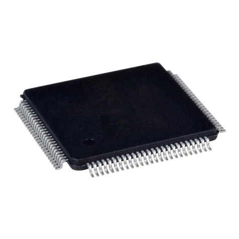
•80-pin QFP14 surface mount package.
*

X26A-C-001-072
GRAPHICS
S1D13704
■SYSTEM BLOCK DIAGRAM
S1D13704
Flat Panel
Data and
CPU Control Signals Digital Out
Actual Size
FOR SYSTEM INTEGRATION SERVICES
FOR WINDOWS® CE CONTACT:
Epson Research & Development, Inc.
Suite #320 - 11120 Horseshoe Way
Richmond, B.C., Canada V7A 5H7
Tel: (604) 275-5151
Fax: (604) 275-2167
Email: [email protected].com
http://www.erd.epson.com
CONTACT YOUR SALES REPRESENTATIVE FOR THESE
COMPREHENSIVE DESIGN TOOLS:
• S1D13704 Technical Manual
• S5U13704 Evaluation Boards
• WindowsCE Display Driver
• CPU Independent Software Utilities
Japan
Seiko Epson Corporation
Electronic Devices Marketing Division
421-8, Hino, Hino-shi
Tokyo 191-8501, Japan
Tel: 042-587-5812
Fax: 042-587-5564
http://www.epson.co.jp
Hong Kong
Epson Hong Kong Ltd.
20/F., Harbour Centre
25 Harbour Road
Wanchai, Hong Kong
Tel: 2585-4600
Fax: 2827-4346
Taiwan, R.O.C.
Epson Taiwan Technology
& Trading Ltd.
10F, No. 287
Nanking East Road
Sec. 3, Taipei, Taiwan, R.O.C.
Tel: 02-2717-7360
Fax: 02-2712-9164
Singapore
Epson Singapore Pte., Ltd.
No. 1
Temasek Avenue #36-00
Millenia Tower
Singapore, 039192
Tel: 337-7911
Fax: 334-2716
Europe
Epson Europe Electronics GmbH
Riesstrasse 15
80992 Munich, Germany
Tel: 089-14005-0
Fax: 089-14005-110
North America
Epson Electronics America, Inc.
150 River Oaks Parkway
San Jose, CA 95134, USA
Tel: (408) 922-0200
Fax: (408) 922-0238
http://www.eea.epson.com
Copyright ©1998, 2001 Epson Research and Development, Inc. All rights reserved. VDC
Information in this document is subject to change without notice. You may download and use this document, but only for your own use in evaluating Seiko Ep-
son/EPSON products. You may not modify the document. Epson Research and Development, Inc. disclaims any representation that the contents of thisdocument
are accurate or current. The Programs/Technologies described in thisdocument may contain material protected under U.S. and/or International Patent laws.
EPSON is a registered trademark of Seiko Epson Corporation. Microsoft, Windows, and the Windows CE Logo are registered trademarks of Microsoft Corporation.
*

S1D13704 Embedded Memory LCD Controller
Hardware Functional Specification
Document Number: X26A-A-001-04
Copyright © 1998, 2001 Epson Research and Development, Inc. All Rights Reserved.
Information in this document is subject to change without notice. Youmay download and use this document, butonly for your own use in
evaluating Seiko Epson/EPSON products. You may not modify the document. Epson Research and Development, Inc. disclaims any
representation that the contents of this document are accurate or current. The Programs/Technologies described in this document may contain
material protected underU.S. and/or InternationalPatent laws.
EPSON is a registered trademark of Seiko Epson Corporation. All other Trademarks are the property of their respective owners
*

Page 2 Epson Research and Development
Vancouver Design Center
S1D13704 Hardware Functional Specification
X26A-A-001-04 Issue Date: 01/02/08
THIS PAGE LEFT BLANK
*

Epson Research and Development Page 3
Vancouver Design Center
Hardware Functional Specification S1D13704
Issue Date: 01/02/08 X26A-A-001-04
Table of Contents
1 Introduction . . . . . . . . . . . . . . . . . . . . . . . . . . . . . . . . . . . . . . . . 9
1.1 Scope . . . . . . . . . . . . . . . . . . . . . . . . . . . . . . . . . . .9
1.2 Overview Description . . . . . . . . . . . . . . . . . . . . . . . . . . . . 9
2 Features . . . . . . . . . . . . . . . . . . . . . . . . . . . . . . . . . . . . . . . . . 10
2.1 Integrated Frame Buffer . . . . . . . . . . . . . . . . . . . . . . . . . . 10
2.2 CPU Interface . . . . . . . . . . . . . . . . . . . . . . . . . . . . . . 10
2.3 Display Support . . . . . . . . . . . . . . . . . . . . . . . . . . . . . . 10
2.4 Display Modes . . . . . . . . . . . . . . . . . . . . . . . . . . . . . . 11
2.5 Clock Source . . . . . . . . . . . . . . . . . . . . . . . . . . . . . . . 11
2.6 Miscellaneous . . . . . . . . . . . . . . . . . . . . . . . . . . . . . . 11
2.7 Package . . . . . . . . . . . . . . . . . . . . . . . . . . . . . . . . . 11
3 Typical System Implementation Diagrams . . . . . . . . . . . . . . . . . . . . . . 12
4 Functional Block Diagram . . . . . . . . . . . . . . . . . . . . . . . . . . . . . . . 15
4.1 Functional Block Descriptions . . . . . . . . . . . . . . . . . . . . . . . . 15
4.1.1 Host Interface . . . . . . . . . . . . . . . . . . . . . . . . . . . . . . . . . . . . . 15
4.1.2 Memory Controller . . . . . . . . . . . . . . . . . . . . . . . . . . . . . . . . . . 15
4.1.3 Sequence Controller . . . . . . . . . . . . . . . . . . . . . . . . . . . . . . . . . . 15
4.1.4 Look-Up Table . . . . . . . . . . . . . . . . . . . . . . . . . . . . . . . . . . . . 16
4.1.5 LCD Interface . . . . . . . . . . . . . . . . . . . . . . . . . . . . . . . . . . . . . 16
4.1.6 Power Save . . . . . . . . . . . . . . . . . . . . . . . . . . . . . . . . . . . . . . 16
5 Pins . . . . . . . . . . . . . . . . . . . . . . . . . . . . . . . . . . . . . . . . . . . 17
5.1 Pinout Diagram . . . . . . . . . . . . . . . . . . . . . . . . . . . . . . 17
5.2 Pin Description . . . . . . . . . . . . . . . . . . . . . . . . . . . . . . 18
5.2.1 Host Interface . . . . . . . . . . . . . . . . . . . . . . . . . . . . . . . . . . . . . 18
5.2.2 LCD Interface . . . . . . . . . . . . . . . . . . . . . . . . . . . . . . . . . . . . . 20
5.2.3 Clock Input . . . . . . . . . . . . . . . . . . . . . . . . . . . . . . . . . . . . . . 21
5.2.4 Miscellaneous . . . . . . . . . . . . . . . . . . . . . . . . . . . . . . . . . . . . . 21
5.2.5 Power Supply . . . . . . . . . . . . . . . . . . . . . . . . . . . . . . . . . . . . . 21
5.3 Summary of Configuration Options . . . . . . . . . . . . . . . . . . . . . . 22
5.4 Host Bus Interface Pin Mapping . . . . . . . . . . . . . . . . . . . . . . . 22
5.5 LCD Interface Pin Mapping . . . . . . . . . . . . . . . . . . . . . . . . . 23
6 D.C. Characteristics . . . . . . . . . . . . . . . . . . . . . . . . . . . . . . . . . . 24
7 A.C. Characteristics . . . . . . . . . . . . . . . . . . . . . . . . . . . . . . . . . . 26
7.1 Bus Interface Timing . . . . . . . . . . . . . . . . . . . . . . . . . . . 26
7.1.1 SH-4 Interface Timing . . . . . . . . . . . . . . . . . . . . . . . . . . . . . . . . 26
7.1.2 SH-3 Interface Timing . . . . . . . . . . . . . . . . . . . . . . . . . . . . . . . . 28
7.1.3 Motorola M68K #1 Interface Timing . . . . . . . . . . . . . . . . . . . . . . . . . 30
*

Page 4 Epson Research and Development
Vancouver Design Center
S1D13704 Hardware Functional Specification
X26A-A-001-04 Issue Date: 01/02/08
7.1.4 Motorola M68K #2 Interface Timing . . . . . . . . . . . . . . . . . . . . . . . . . 31
7.1.5 Generic #1 Interface Timing . . . . . . . . . . . . . . . . . . . . . . . . . . . . . . 32
7.1.6 Generic #2 Interface Timing . . . . . . . . . . . . . . . . . . . . . . . . . . . . . . 33
7.2 Clock Input Requirements . . . . . . . . . . . . . . . . . . . . . . . . . .34
7.3 Display Interface . . . . . . . . . . . . . . . . . . . . . . . . . . . . . .35
7.3.1 Power On/Reset Timing . . . . . . . . . . . . . . . . . . . . . . . . . . . . . . . . 35
7.3.2 Power Down/Up Timing . . . . . . . . . . . . . . . . . . . . . . . . . . . . . . . 36
7.3.3 Single Monochrome 4-Bit Panel Timing . . . . . . . . . . . . . . . . . . . . . . . 37
7.3.4 Single Monochrome 8-Bit Panel Timing . . . . . . . . . . . . . . . . . . . . . . . 39
7.3.5 Single Color 4-Bit Panel Timing . . . . . . . . . . . . . . . . . . . . . . . . . . . 41
7.3.6 Single Color 8-Bit Panel Timing (Format 1) . . . . . . . . . . . . . . . . . . . . . 43
7.3.7 Single Color 8-Bit Panel Timing (Format 2) . . . . . . . . . . . . . . . . . . . . . 45
7.3.8 Dual Monochrome 8-Bit Panel Timing . . . . . . . . . . . . . . . . . . . . . . . . 47
7.3.9 Dual Color 8-Bit Panel Timing . . . . . . . . . . . . . . . . . . . . . . . . . . . . 49
7.3.10 9/12-Bit TFT/D-TFD Panel Timing . . . . . . . . . . . . . . . . . . . . . . . . . . 51
8 Registers . . . . . . . . . . . . . . . . . . . . . . . . . . . . . . . . . . . . . . . . .54
8.1 Register Mapping . . . . . . . . . . . . . . . . . . . . . . . . . . . . . 54
8.2 Register Descriptions . . . . . . . . . . . . . . . . . . . . . . . . . . . .54
9 Frame Rate Calculation . . . . . . . . . . . . . . . . . . . . . . . . . . . . . . . . .70
10 Display Data Formats . . . . . . . . . . . . . . . . . . . . . . . . . . . . . . . . . .71
11 Look-Up Table Architecture . . . . . . . . . . . . . . . . . . . . . . . . . . . . . . .72
11.1 Gray Shade Display Modes . . . . . . . . . . . . . . . . . . . . . . . . . .72
11.2 Color Display Modes . . . . . . . . . . . . . . . . . . . . . . . . . . . .75
12 SwivelView™ . . . . . . . . . . . . . . . . . . . . . . . . . . . . . . . . . . . . . . .79
12.1 Default SwivelView Mode . . . . . . . . . . . . . . . . . . . . . . . . . .79
12.1.1 How to Set Up Default SwivelView Mode . . . . . . . . . . . . . . . . . . . . . . 80
12.2 Alternate SwivelView Mode . . . . . . . . . . . . . . . . . . . . . . . . .81
12.2.1 How to Set Up Alternate SwivelView Mode . . . . . . . . . . . . . . . . . . . . . 82
12.3 Comparison Between Default and Alternate SwivelView Modes . . . . . . . . . . .83
12.4 SwivelView Mode Limitations . . . . . . . . . . . . . . . . . . . . . . . .83
13 Power Save Modes . . . . . . . . . . . . . . . . . . . . . . . . . . . . . . . . . . . .84
13.1 Software Power Save Mode . . . . . . . . . . . . . . . . . . . . . . . . .84
13.2 Hardware Power Save Mode . . . . . . . . . . . . . . . . . . . . . . . . .84
13.3 Power Save Mode Function Summary . . . . . . . . . . . . . . . . . . . . .85
13.4 Panel Power Up/Down Sequence . . . . . . . . . . . . . . . . . . . . . . .85
13.5 Turning Off BCLK Between Accesses . . . . . . . . . . . . . . . . . . . . .86
13.6 Clock Requirements . . . . . . . . . . . . . . . . . . . . . . . . . . . .87
14 Mechanical Data . . . . . . . . . . . . . . . . . . . . . . . . . . . . . . . . . . . . .88
*

Epson Research and Development Page 5
Vancouver Design Center
Hardware Functional Specification S1D13704
Issue Date: 01/02/08 X26A-A-001-04
List of Tables
Table 5-1: Summary of Power On/Reset Options . . . . . . . . . . . . . . . . . . . . . . . . . . . 22
Table 5-2: Host Bus Interface Pin Mapping . . . . . . . . . . . . . . . . . . . . . . . . . . . . . . 22
Table 5-3: LCD Interface Pin Mapping . . . . . . . . . . . . . . . . . . . . . . . . . . . . . . . . 23
Table 6-1: Absolute Maximum Ratings . . . . . . . . . . . . . . . . . . . . . . . . . . . . . . . . 24
Table 6-2: Recommended Operating Conditions . . . . . . . . . . . . . . . . . . . . . . . . . . . 24
Table 6-3: Input Specifications . . . . . . . . . . . . . . . . . . . . . . . . . . . . . . . . . . . . 24
Table 6-4: Output Specifications. . . . . . . . . . . . . . . . . . . . . . . . . . . . . . . . . . . . 25
Table 7-1: SH-4 Timing . . . . . . . . . . . . . . . . . . . . . . . . . . . . . . . . . . . . . . . . 27
Table 7-2: SH-3 Bus Timing. . . . . . . . . . . . . . . . . . . . . . . . . . . . . . . . . . . . . . 29
Table 7-3: M68K #1 Bus Timing (MC68000) . . . . . . . . . . . . . . . . . . . . . . . . . . . . 30
Table 7-4: M68K #2 Timing (MC68030) . . . . . . . . . . . . . . . . . . . . . . . . . . . . . . . 31
Table 7-5: Generic #1 Timing . . . . . . . . . . . . . . . . . . . . . . . . . . . . . . . . . . . . . 32
Table 7-6: Generic #2 Timing . . . . . . . . . . . . . . . . . . . . . . . . . . . . . . . . . . . . . 33
Table 7-7: Clock Input Requirements . . . . . . . . . . . . . . . . . . . . . . . . . . . . . . . . . 34
Table 7-8: Power Down/Up Timing . . . . . . . . . . . . . . . . . . . . . . . . . . . . . . . . . . 36
Table 8-1: Panel Data Format . . . . . . . . . . . . . . . . . . . . . . . . . . . . . . . . . . . . . 55
Table 8-2: Gray Shade/Color Mode Selection. . . . . . . . . . . . . . . . . . . . . . . . . . . . . 56
Table 8-3: High Performance Selection . . . . . . . . . . . . . . . . . . . . . . . . . . . . . . . . 56
Table 8-4: Inverse Video Mode Select Options . . . . . . . . . . . . . . . . . . . . . . . . . . . . 57
Table 8-5: Hardware Power Save/GPIO0 Operation . . . . . . . . . . . . . . . . . . . . . . . . . 58
Table 8-6: Software Power Save Mode Selection . . . . . . . . . . . . . . . . . . . . . . . . . . . 58
Table 8-7: Look-Up Table Access . . . . . . . . . . . . . . . . . . . . . . . . . . . . . . . . . . . 65
Table 8-8: Selection of SwivelView Mode . . . . . . . . . . . . . . . . . . . . . . . . . . . . . . 68
Table 8-9: Selection of PCLK and MCLK in SwivelView Mode . . . . . . . . . . . . . . . . . . . 69
Table 11-1: Look-Up Table Configurations. . . . . . . . . . . . . . . . . . . . . . . . . . . . . . . 72
Table 12-1: Default and Alternate SwivelView Mode Comparison . . . . . . . . . . . . . . . . . . 83
Table 13-1: Power Save Mode Selection . . . . . . . . . . . . . . . . . . . . . . . . . . . . . . . . 84
Table 13-2: Software Power Save Mode Summary. . . . . . . . . . . . . . . . . . . . . . . . . . . 84
Table 13-3: Hardware Power Save Mode Summary . . . . . . . . . . . . . . . . . . . . . . . . . . 84
Table 13-4: Power Save Mode Function Summary . . . . . . . . . . . . . . . . . . . . . . . . . . . 85
Table 13-5: S1D13704 Internal Clock Requirements. . . . . . . . . . . . . . . . . . . . . . . . . . 87
*

Page 6 Epson Research and Development
Vancouver Design Center
S1D13704 Hardware Functional Specification
X26A-A-001-04 Issue Date: 01/02/08
THIS PAGE LEFT BLANK
*

Epson Research and Development Page 7
Vancouver Design Center
Hardware Functional Specification S1D13704
Issue Date: 01/02/08 X26A-A-001-04
List of Figures
Figure 3-1: Typical System Diagram (SH-4 Bus). . . . . . . . . . . . . . . . . . . . . . . . . . . . 12
Figure 3-2: Typical System Diagram (SH-3 Bus). . . . . . . . . . . . . . . . . . . . . . . . . . . . 12
Figure 3-3: Typical System Diagram (M68K #1 Bus) . . . . . . . . . . . . . . . . . . . . . . . . . 13
Figure 3-4: Typical System Diagram (M68K #2 Bus) . . . . . . . . . . . . . . . . . . . . . . . . . 13
Figure 3-5: Typical System Diagram (Generic #1 Bus) . . . . . . . . . . . . . . . . . . . . . . . . 14
Figure 3-6: Typical System Diagram (Generic #2 Bus - e.g. ISA Bus). . . . . . . . . . . . . . . . . 14
Figure 4-1: System Block Diagram Showing Data Paths. . . . . . . . . . . . . . . . . . . . . . . . 15
Figure 5-1: Pinout Diagram . . . . . . . . . . . . . . . . . . . . . . . . . . . . . . . . . . . . . . . 17
Figure 7-1: SH-4 Timing . . . . . . . . . . . . . . . . . . . . . . . . . . . . . . . . . . . . . . . . 26
Figure 7-2: SH-3 Bus Timing . . . . . . . . . . . . . . . . . . . . . . . . . . . . . . . . . . . . . . 28
Figure 7-3: M68K #1 Bus Timing (MC68000) . . . . . . . . . . . . . . . . . . . . . . . . . . . . . 30
Figure 7-4: M68K #2 Timing (MC68030) . . . . . . . . . . . . . . . . . . . . . . . . . . . . . . .31
Figure 7-5: Generic #1 Timing . . . . . . . . . . . . . . . . . . . . . . . . . . . . . . . . . . . . . 32
Figure 7-6: Generic #2 Timing . . . . . . . . . . . . . . . . . . . . . . . . . . . . . . . . . . . . . 33
Figure 7-7: Clock Input Requirements . . . . . . . . . . . . . . . . . . . . . . . . . . . . . . . . . 34
Figure 7-8: LCD Panel Power On/Reset Timing . . . . . . . . . . . . . . . . . . . . . . . . . . . . 35
Figure 7-9: Power Down/Up Timing . . . . . . . . . . . . . . . . . . . . . . . . . . . . . . . . . . 36
Figure 7-10: Single Monochrome 4-Bit Panel Timing. . . . . . . . . . . . . . . . . . . . . . . . . . 37
Figure 7-11: Single Monochrome 4-Bit Panel A.C. Timing . . . . . . . . . . . . . . . . . . . . . . . 38
Figure 7-12: Single Monochrome 8-Bit Panel Timing. . . . . . . . . . . . . . . . . . . . . . . . . . 39
Figure 7-13: Single Monochrome 8-Bit Panel A.C. Timing . . . . . . . . . . . . . . . . . . . . . . . 40
Figure 7-14: Single Color 4-Bit Panel Timing . . . . . . . . . . . . . . . . . . . . . . . . . . . . . . 41
Figure 7-15: Single Color 4-Bit Panel A.C. Timing . . . . . . . . . . . . . . . . . . . . . . . . . . .42
Figure 7-16: Single Color 8-Bit Panel Timing (Format 1) . . . . . . . . . . . . . . . . . . . . . . . . 43
Figure 7-17: Single Color 8-Bit Panel A.C. Timing (Format 1) . . . . . . . . . . . . . . . . . . . . . 44
Figure 7-18: Single Color 8-Bit Panel Timing (Format 2) . . . . . . . . . . . . . . . . . . . . . . . . 45
Figure 7-19: Single Color 8-Bit Panel A.C. Timing (Format 2) . . . . . . . . . . . . . . . . . . . . . 46
Figure 7-20: Dual Monochrome 8-Bit Panel Timing. . . . . . . . . . . . . . . . . . . . . . . . . . . 47
Figure 7-21: Dual Monochrome 8-Bit Panel A.C. Timing. . . . . . . . . . . . . . . . . . . . . . . . 48
Figure 7-22: Dual Color 8-Bit Panel Timing . . . . . . . . . . . . . . . . . . . . . . . . . . . . . . . 49
Figure 7-23: Dual Color 8-Bit Panel A.C. Timing . . . . . . . . . . . . . . . . . . . . . . . . . . . .50
Figure 7-24: 12-Bit TFT/D-TFD Panel Timing . . . . . . . . . . . . . . . . . . . . . . . . . . . . .51
Figure 7-25: TFT/D-TFD A.C. Timing. . . . . . . . . . . . . . . . . . . . . . . . . . . . . . . . . . 52
Figure 8-1: Screen-Register Relationship, Split Screen. . . . . . . . . . . . . . . . . . . . . . . . . 64
Figure 10-1: 1/2/4/8 Bit-Per-Pixel Display Data Memory Organization. . . . . . . . . . . . . . . . . 71
Figure 11-1: 2-Level Gray-Shade Mode Look-Up Table Architecture . . . . . . . . . . . . . . . . . 72
Figure 11-2: 4-Level Gray-Shade Mode Look-Up Table Architecture . . . . . . . . . . . . . . . . . 73
*

Page 8 Epson Research and Development
Vancouver Design Center
S1D13704 Hardware Functional Specification
X26A-A-001-04 Issue Date: 01/02/08
Figure 11-3: 16-Level Gray-Shade Mode Look-Up Table Architecture . . . . . . . . . . . . . . . . . 73
Figure 11-4: Look-Up Table Bypass Mode Architecture. . . . . . . . . . . . . . . . . . . . . . . . . 74
Figure 11-5: 2-Level Color Look-Up Table Architecture . . . . . . . . . . . . . . . . . . . . . . . . 75
Figure 11-6: 4-Level Color Mode Look-Up Table Architecture . . . . . . . . . . . . . . . . . . . . . 76
Figure 11-7: 16-Level Color Mode Look-Up Table Architecture . . . . . . . . . . . . . . . . . . . . 77
Figure 11-8: 256-Level Color Mode Look-Up Table Architecture. . . . . . . . . . . . . . . . . . . . 78
Figure 12-1: Relationship Between The Screen Image and the Image Refreshed by S1D13704 . . . .79
Figure 12-2: Relationship Between The Screen Image and the Image Refreshed by S1D13704 . . . .81
Figure 13-1: Panel On/Off Sequence . . . . . . . . . . . . . . . . . . . . . . . . . . . . . . . . . . . 86
Figure 14-1: Mechanical Drawing QFP14 . . . . . . . . . . . . . . . . . . . . . . . . . . . . . . . . 88
*

Epson Research and Development Page 9
Vancouver Design Center
Hardware Functional Specification S1D13704
Issue Date: 01/02/08 X26A-A-001-04
1 Introduction
1.1 Scope
This is the Functional Specification for the S1D13704 Embedded Memory LCD Controller
Chip. Included in this document are timing diagrams, AC and DC characteristics, register
descriptions, and power management descriptions. This document is intended for two
audiences: Video Subsystem Designers and Software Developers.
Please check the Epson Electronics America website at http://www.eea.epson.com for the
latest revision of this document before beginning any development.
We appreciate your comments on our documentation. Please contact us via email at
techpubs@erd.epson.com.
1.2 Overview Description
The S1D13704 is a color / monochrome LCD graphics controller with an embedded 40K
Byte SRAM display buffer. The high integration of the S1D13704 provides a low cost, low
power, single chip solution to meet the requirements of embedded markets such as Office
Automation equipment, Mobile Communications devices, and Hand-Held PCs where
board size and battery life are major concerns.
Products requiring a “Portrait” display can take advantage of the Swivelview™ (90°
Hardware Rotate) feature of the S1D13704. Virtual and Split Screen are just some of the
display modes supported. The above features, combined with the Operating System
independence of the S1D13704, make it the ideal solution for a wide variety of applica-
tions.
*

Page 10 Epson Research and Development
Vancouver Design Center
S1D13704 Hardware Functional Specification
X26A-A-001-04 Issue Date: 01/02/08
2 Features
2.1 Integrated Frame Buffer
• Embedded 40K byte SRAM display buffer.
2.2 CPU Interface
• Direct support of the following interfaces:
Hitachi SH-3.
Hitachi SH-4.
Motorola M68K.
MPU bus interface using WAIT# signal.
• Direct memory mapping of internal registers.
• Single level CPU write buffer.
• Registers are mapped into upper 32 bytes of 64K byte address space.
• The complete 40K byte frame buffer is directly and contiguously available through the
16-bit address bus.
2.3 Display Support
• 4/8-bit monochrome LCD interface.
• 4/8-bit color LCD interface.
• Single-panel, single-drive passive displays.
• Dual-panel, dual-drive passive displays.
• Active Matrix TFT / D-TFD interface
• Register level support for EL panels.
• Example resolutions:
640x480 at a color depth of 1 bpp
640x240 at a color depth of 2 bpp
320x240 at a color depth of 4 bpp
240x160 at a color depth of 8 bpp
*

Epson Research and Development Page 11
Vancouver Design Center
Hardware Functional Specification S1D13704
Issue Date: 01/02/08 X26A-A-001-04
2.4 Display Modes
• SwivelView™: direct 90° hardware rotation of display image for portrait mode display.
• 1/2/4 bit-per-pixel (bpp), 2/4/16-level grayshade display.
• 1/2/4/8 bit-per-pixel, 2/4/16/256-level color display.
• Up to 16 shades of gray by FRM on monochrome passive LCD panels; a 16x4 Look-
Up-Table is used to map 1/2/4-bpp modes into these shades.
• 256 simultaneous of 4096 colors on color passive and active matrix LCD panels; three
16x4 Look-Up Tables are used to map 1/2/4/8-bpp modes into these colors.
• Split screen display for all landscape panel modes allows two different images to be
simultaneously displayed.
• Virtual display support (displays images larger than the panel size through the use of
panning).
2.5 Clock Source
• Maximum operating clock (CLK) frequency of 25MHz.
• Operating clock (CLK) is derived from CLKI input.
CLK = CLKI
or
CLK = CLKI/2
• Pixel Clock (PCLK) and Memory Clock (MCLK) are derived from CLK.
2.6 Miscellaneous
• Hardware/Software Video Invert.
• Software Power Save mode.
• Hardware Power Save mode.
• LCD power-down sequencing.
• 5 General Purpose Input/Output pins are available.
• GPIO0 is available if Hardware Power Save is not required.
• GPIO[4:1] are available if upper LCD data pins (FPDAT[11:8]) are not required for
TFT/D-TFD support or Hardware Video Invert.
• IO Operates from 3.0 volts to 5.5 volts
• Core operates from 3.0 volts to 3.6 volts.
2.7 Package
• 80 pin QFP14 package.
*

Page 12 Epson Research and Development
Vancouver Design Center
S1D13704 Hardware Functional Specification
X26A-A-001-04 Issue Date: 01/02/08
3 Typical System Implementation Diagrams
.
Figure 3-1: Typical System Diagram (SH-4 Bus)
.
Figure 3-2: Typical System Diagram (SH-3 Bus)
S1D13704 FPFRAME
FPSHIFT
FPLINE
DRDY
FPDAT[7:0]
CLKI
Oscillator
FPFRAME
FPSHIFT
FPLINE
MOD
D[7:0]
8-bit
LCD
Display
SH-4
BUS
RESET#
WE0#
D[15:0]
BS#
RD/WR#
RD#
RDY#
A[15:0]
CKIO
WE0#
RD/WR#
AB[15:0]
DB[15:0]
WE1#
BS#
RD#
CS#
BCLK
WAIT#
RESET#
CSn#
WE1#
LCDPWR
S1D13704 FPFRAME
FPSHIFT
FPLINE
DRDY
FPDAT[3:0]
CLKI
Oscillator
FPFRAME
FPSHIFT
FPLINE
MOD
D[3:0]
4-bit
LCD
Display
SH-3
BUS
RESET#
WE0#
D[15:0]
BS#
RD/WR#
RD#
WAIT#
A[15:0]
CKIO
WE0#
RD/WR#
AB[15:0]
DB[15:0]
WE1#
BS#
RD#
CS#
BCLK
WAIT#
RESET#
CSn#
WE1#
LCDPWR
*
Table of contents
Other Epson Controllers manuals

Epson
Epson S1D13503 Series User manual

Epson
Epson BO-IC400 User manual

Epson
Epson S1D13505F00A User manual

Epson
Epson RC700 User manual

Epson
Epson TP3 User manual

Epson
Epson RC90 User manual

Epson
Epson RC520 User manual

Epson
Epson RC90 User manual

Epson
Epson S1R72U16 Installation instructions

Epson
Epson RC620 Series Manual
Popular Controllers manuals by other brands

Iron logic
Iron logic Matrix III 220 user manual

flakt woods
flakt woods STRA-24 Installation and commissioning manual

Timeguard
Timeguard TRT039N Installation & operating instructions

Securakey
Securakey SURE-FI SK-DS004-WIEGAND Operator's manual

Pro2
Pro2 VWC33 operating instructions

Audio Control
Audio Control MVC Owner's enjoyment manual