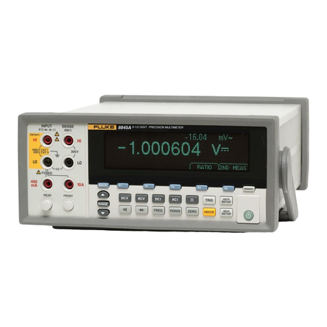
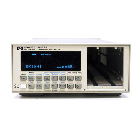
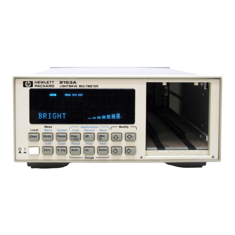
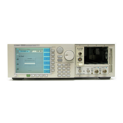
HP 8153A User manual

HP 8 153A
Ligh,~"lI,av~:;M~ltimeter/".:",:" ..
=:..
'.' '. ' <~.'-'~••: -. .. "."
SERIAL NUMBERS
This manual applies to all instruments
,., -~ > .
..1
HP
Part
No.
'08153~90001
Printed in the Federal Republic of Germany
First Edition
E0592

ì

Service Manual
HP 8153A Lightwave Multimeter
SERIAL NUMBERS
This manual applies to all instruments
Fli;
HEWLETT
~~ PACKARD
HP Part No. 08153-90001
Printed in the Federal Republic of Germany
First Edition
E0592

This document contains proprietary information
w
h
i
eh is protected by copyright. AH rights are
reserved.
No part of this document may be photocopied,
reprc
duced, or translated to another la.ngua.ge
without the prior written consent of
Hewlett-P"ckard GmbH.
©
Copyright 1992 by:
Hewlet
e-Packard GmbH
Herrenberger Str. 130
1030 Boeblingen
Federal Republic of Germany
Subjeet Matter
The information in this document
i
s subject to
change without no
t
ice.
Hewlett-Packard makes
no
warranty of any
kind with regard to this printed material
including but not limited to the implied
warranties of merchantability and fitness
for
a
particular purpose.
HewleU-Packard ahall not be liable for errors
contained herein or for incidental or
consequential da.mages in connection with the
furnishing,
perfor-mance,
or use of this mat erial.
Printing History
New editions are complete revisions of the
manuaì. Update pa.ckages, conta.in additional
and repl acement informa.tion to be incorporated
into the manual by the customer. The date on
the title page only changes when a new manual is
published. When an edition is reprinted, all the
prior up dat es to the edition are incorporated.
Control Serial Number: First Edition ap pl ies
directly to aH instruments.
Prelimina.ry Ediiion : 1st May 1992 :
08153-90031 : E0592
Funkentstorung Deutschland
Notices
Warranty
This Hewlett-Pa.ckard
i
ns
t
rumen
t
product is
warranted against defects in
ma
t
er
i
al and
workmanship for a period of one
year
from date of
shipment . During the warranty pe ric d, HP will,
at
i
t
s option, either
rep
a.ir or
repl
ace
pr
cduc ts
which prove to be defective.
For warranty service or repai
t,
t
h
i
s product rnus
t
be returned to a service facility designated by HP.
Buyer shaIl prepay shipping charges to HP and
HP ahe.Il pay shipping charges to return the
product to Buyer. Hcwever, Buyer shall pay all
shipping char ges, duties, and taxes for pro duc
t
s
returned to HP from another country.
HP warrants that its software and
fì
rmwàre
designated by HP for use with an instrument will
execute
i
t
s programming instructions when
properly
.i
ns
t
alled on that instrument. HP dc es
not warrant that the operation of the instrument,
software, or
fì
rrnwar e will be uninterrupted or
errcr free.
Limitation of Warranty
The foregoing warranty shall not ap plyto defects
resulting from
i
mprop er or inadequate
maintenance by Buyer, Bu yer-suppfied software or
interfacing, unauthorized modification or misuse,
operation outside of the environmental
specifications for the product, or improper site
prepa.ration or maintenance.
No other warranty
i
s expressed or
i
mplied.
Hewlet t-Packard specifically disda.ims the implied
warranties of Merchanta.bility au.d Fitness for a
Per sicular Purpose.
Exclusive Rernedies
The remedies provided herein
ar
e
Bu
yer+s sole
and
e
xc
ì
usive
r
ernedies.
Hewle
et-Packard shall
ne
t
be liable for a.ny direct ,
i
rrd'irect , speclal,
incidental, or
ccns
equ ential
d
amages whether
based on
co
ntrac
t ,
tort, or any
o
t
her lega.l
theory.
Assistance
Product maintenance agreements and other
customer aas.is
t
a.nce agreements are available fcr
Hewl eet-Packar d products. For any aasis
t
a.nce
contact your nearest Hewlett-Packard Sales and
Service Office. Addresses are provided at
t
he
back of
t
his manua.l.
Certification
Hewle
t
r-Packard Company certifies that
t
his
product met
i
t
s published specifications at the
time ci shipment from the fa.ctory.
Hewle
t
t-P'acka.rd further certifies
t
ha
t
its
cal
i
brat
i
on me aau remen
t
s are traceable to the
United States Nationa.l Institute cf Standards
an
d
Technology, NIST (formerly the United
Sta
t
es National Bureau of Stendards , NBS) to
t
he exrent allowed by th e Institutes's calibration
facil
it
y,
and to the calibration facilities of other
International Sta.ndards Orga.niza.tion members.
Electrornagnetic Interference Regulations, Gerrnany
Dieses Gerà.t wurde in einer typischen Systemkonfiguration gepriift und
entspricht den Bestimmungen der Allgemeinen Genehmigung FTZ
1046/84.
Ah
Nachweis
i
s
t
das Gera.t mit dem VDE-Funkschutzzeichen
gekennzeichnet.
This devi ce was
t
eated in a
t
y
pica.l system confì gurat ion and meets the
GeneraI License requirements in Germany (FTZ 1046/84). As a proof of
compliance
ii
carries the VDE Radio Protection Mark
Safety Considerations
The Model HP 8I53A is a Class 1 instrument (that is, an instrument
with an exposed metal chassis directly connected to earth via the
power supply cable). The symbol used to show a protective earth
terminal in the instrument is ~ .
Before operation, you should review the instrument and manual,
including the red safety page, for safety markings and instructions.
You must follow these to ensure safe operation and to maintain the
instrument in safe condition.
Some HP 8I53A circuits are powered whenever the instrument is
connected to the AC power source. To disconnect from the line
power , disconnect the power cord either at the rear power-inlet or at
the AC line-power source (receptacle). One of these must always be
accessible. If the instrument is in a cabinet, it must be disconnected
from the line power by the system's line-power switch.
Initial Inspection
Inspect the shipping container for damage. If there is damage to
the container or cushioning, you should keep them until you have
checked the contents of the shipment for completeness and verified
the instrument both mechanically and electricaliy.
The Performance Tests give procedures for checking the operation of
the instrument. If the contents are incomplete, mechanical damage or
defect is apparent , or if an instrument does not pass the operator's
checks, notify the nearest Hewlett-Packard office.
Warning To avoid hazardous electrical shock, do not perform electrical tests
when there are signs of shipping damage to any portion of the outer
enclosure (covers, panels,
etc.),
Line Power Requirements
The HP 8I53A can operate from any single-phase AC power source
that supplies between 100V and 240V at a frequency in the range
from 40 to 60Hz. The maximum power consumption is 55VA with ali
options instalied.
The fuse used by this instrument is TIA / 250V (slow) (HP Part No.
2110-0007). This fuse is located on the power supply board.
iii

Line Power Cable
Warning
iv
In accordance with international safety standards, this instrument
has a three-wire power cable. When connected to an appropriate AC
power receptacle, this cable earths the instrument cabinet. The type
of power cable shipped with each instrument depends on the country
of destination. Refer to Figure
Q-l
for the part numbers of the power
cables available.
To avoid the possibility of injury or death, you must observe the
following precautions before switching on the instrument.
• If this instrument is to be energized via an autotransformer for
voltage reduction, ensure that the Common terminai connects to the
earthed pole of the power source.
• Insert the power cable plug only into a socket outlet provided with a
protective earth contact. Do not negate this protective action by the
using an extension cord without a protective conductor.
• Before switching on the instrument, the protective earth terminai of
the instrument must be connected to a protective conductor. You
can do this by using the power cord supplied with the instrument.
• It is prohibited to interrupt the protective earth connection
intentionally.

I
o
lE
L
E
[]]
~E~ ••
L
--
E
L
N
•
Rustral la
Ilerima
r
k
Europe Great Br
r
t
a
i
o
8120-1359 8120-1589 8120-1351
South Hf r
r
c a
8120-4211 ~
~
SWltzerland
8120-2104
Figure 0-1. Une Power Cables - Plug Identification
~
L
NI
Unlted States
E 120V
• 8120-1378
The following work should be carried out by a qualified electrician,

and all local electrical codes must be strictly observed. If the plug
on the cable does not fit the power outlet, or if the cable is to be
attached to a terminal block, cut the cable at the plug end and
rewire it.
The color coding used in the cable depends on the cable supplied.
If you are connecting a new plug, it should meet the local safety
requirements and include the following features:
• Adequate load-carrying capacity (see table of specifications).
• Ground connection.
• Cable clamp.
Operating Environment
The following summarizes the
HP
8153A operating environment
ranges. In order for the
HP
8153A to meet specifications, the
operating environment must be within these limits.
Warning The HP 8153A is not designed for outdoor use. To prevent potential
fire or shock hazard, do not expose the HP 8153A to rain or other

excessive moisture.
Temperature
The
HP
8153A may be operated in temperatures from O°C to 55°C.
v

Hurnidity
Instrurnent Cooling
InputjOutput Signals
Caution
,
Storage and Shiprnent
vi
The HP 8153A may be operated in environments with humidity up
to 95% (O°C to +40°C). The HP 8153A should be protected from
temperatures or temperature changes that cause condensation within
the instrument.
The HP 8153A has a cooling fan mounted internally. Mount or
position the instrument so that air can circulate through it freely.
When operating the HP 8153A, choose a location that provides at
least 75mm (3inches) of clearance at the rear, and at least 25mm
(linch) of clearance at each side. Failure to provide adequate air
clearance may result in excessive internal temperature, reducing
instrument reliability.
A maximum of 15V can be applied as an external voltage to any of
the BNC connectors.
The instrument can be stored or shipped at temperatures between
-40°C and +70°C. The instrument should be protected from
temperature extremes that may cause condensation within it.
-

Initial Safety Infarmatian far Laser Source Madules
The Specifications for these modules are as follows:
HP 81551MM HP 81552SM HP 81553SM HP 81554SM
Laser Type FP-Laser FP-Laser FP-Laser Dual FP-Laser
InGaAsP InGaAsP InGaAsP InGaAsP
Laser Class
According to IEC 825 3A 3A 3A 3A
(Europe)
According to 21 CFR 1040.10
l
1 1 1
(Canada, Japan, USA)
Output Power >-2dBm >OdBm >OdBm >-ldBm
Beam Diameter
50/Lm 9/Lm 9/Lm 9/Lm
Numerical Aperture 0.2 0.1 0.1 0.1
Wavelength 850±10nrn 1310±20nrn 1550±20nm 1310/1550±20nm
Note
Canada, Japan, USA
C lass
Laser Product
The laser safety warning labels are included with the laser module.
You
MUST
stick these labels onto the outside of the mainframe,
in a position where they are clearly visible to anyone using the
instrument.
Note Europe
CLASS A UR5ER PRODUCT
INVISI~ L~SER R~D MTrON
DO NOT
STRR~
INTO BEAM OR
V ~
DIRECTLY WITH OPTICRL INSTRUMENTS
A sheet of laser safety warning labels are included with the laser
module. You
MUST
stick the labels in the locallanguage onto the
outside of the mainframe, in a position where they are clearly visible
to anyone using the instrument.
You
MUST
return instruments with malfunctioning laser boxes to a
HP Service Center for repair and calibration.
The laser module has built in safety cìrcuitry that will disable the
optical output in the case of a fault condition.
vii

Warning Use of controls or adjustments or performance of procedures other
than those specified for the laser source may result in hazardous
radiation exposure.
Warning Refer Servicing only to qualified and authorized personnel.
Warning Do not enable the laser when there is no fiber attached to the optical
output connector.
The optical output connector is at the bottom, on the laser module
front panel.
The laser is enabled by pressing the grey button above the optical
output connector on the front panel. The laser is enabled when the
green LED on the front panel of the laser module is Iit.
Warning Under no circumstances look into the end of an optical cable attached
to the optical output when the device is operational.
The laser radiation is not visible to the human eye, but it can seriously
damage your eyesight.
Introduction
This manual is arranged into four categories:
• Descriptions of theory of operation. Chapter 1.
• Functional tests and troubleshooting information. Chapters 2, 3,
and 4.
• Component Level Information Package (optional).
P/N
o
f/,
~J - ~
.:><;)0]'
This consists of
o
the circuit diagrams,
o the board layouts, and
o the replaceable parts lists.
-
viii

Contents
1. Theory of Operation
Processor Board Description . . . . . . . 1-1
Clock Generator (U107, U110) . . . . . 1-1
Reset Circuit (U109) with Buffers (U104) 1-1
Central Processor Unit (U101) with PAL (U106),
Address Decoder (U105) and Interface Control
(U103, U104) . . . . . . . 1-1
Memories and Battery Supplies 1-2
EPROMs, . . . . . . 1-2
RAM. . . . . . . . 1-2
Battery Buffered RAM 1-2
Device-Bus Interface 1-2
HP-IB, Real Time Clock and InterfacejCIock
Selection . . . 1-3
HP-IB 1-3
Real Time Clock . . . . 1-3
InterfacejCIock Selection 1-3
Display jKeyboardjInterrupt Interface . 1-3
Interrupts . . . . . . .. .. 1-3
Keyboard Control . . . . 1-4
Display Data and Brightness 1-4
Display Voltage Supply 1-4
Power Supply
Board
1-4
Primary
regulation . . . . 1-4
Secondary regulation . . . 1-5
Overvoltage Protection and Low Voltage Detection 1-5
Display Board . . . . . . . . . . . . . . . . . 1-5
2. Functional Tests
Specifìcations ..... 2-1
Mainframe Specifìcations 2-1
Function Tests . . . . 2-2
Introduction . . . . 2-2
Equipment Required 2-2
Test Record . . . . 2-3
Test Failure . . . . 2-3
Instruments Specifìcations 2-3
IA. Function Test Using the HP 81533A . 2-3
Display Function and Module Interface Tests . 2-4
Display Function Tests . . 2-4
Module Interface Tests 2-4
ANALOG INPUT (8152A IN) 2-6
Contents-1

P.CTRL. . . . . . . . . . . . . . . . . . 2-6
IB. Function Test using a HP 81530/31/32 or HP
81536A Sensor Module. 2-7
HP-IB Interface Test (Optional) . . . . . 2-7
3. Assembling and Disassembling the Instrument
Removing the Instrument Housing . 3-1
Removing the Front Panel Assembly 3-1
Removing the Power Supply Board 3-2
Removing the Processor Board 3-2
Removing the Mother Board 3-3
Removing the Fan Assembly 3-3
4. Troubleshooting
GeneraI . . . . . . . . . . . . . . . . . 4-1
Troubleshooting the A3 Power Supply Board . 4-2
Preparing to Check Power Supply Voltages 4-2
Checking Power Supply Voltages . . . 4-2
Adjusting the Power Supply . . . . . 4-3
Troubleshooting the Al Processor Board 4-4
Before You Start . . . . . . . . . 4-4
Running in Free Run Mode . . . . . 4-4
Troubleshooting in Free Run Mode . 4-5
Troubleshooting the Battery Buffered RAM Supply 4-6
Troubleshooting the VFD Voltage Supply . . . . 4-7
Index
Contents-2
-

O-l. Line Power Cables - Plug Identification
4-1. Pulse at UI02 pin 3. . . . . .
4-2. Pulse at UI02 pin 2. . . . . .
4-3. Pulses from LAS and DETACK
4-4. Pulses from U603 and T601 . .
v
4-3
4-3
4-4
4-7
Figures
Contents-3


1
I
Theory of Operation
Processor Board Description
This information deals with schematics lA to lE.
Clock Generator (U107, U110)
UI07 generates a 16MHz clock signal (CLK16). This is divided by 2
and 4 by U110, to generate the 811Hz clock signal (CLK8) and the
4MHz clock signal (CLK4).
CLK16 is used as the clock for the display Gate Array,
CLK4 clocks the HP-IB interface circuit (schematic lD).
CLK8 is used to clock the Processar UlOl, the PAL Ul06 and the
Device Bus interface circuits (schematic lC).
Reset Circuit (U109) with Buffers (U104)
Ul09 senses the +5 Volt supply voltage during power up.
Until the supply voltage comes above approximately 4.8 Volts, Ul09
activates the reset signal. When the threshold value is reached , the
reset is removed, after a short delay, and the correct start conditions
are established on the processor board.
In the case of a supply voltage drop during normal operation, or if
the supply voltage is switched off, a power down reset signal (LPOR)
is generated which stops further signal processing, switches off the
address decoder and turns on the battery supply for the real time
clock and battery buffered RAMs.
The CPU (UlOl) is a 16/32 bit processor with an 8 bit data bus.
Signals LAS /LDS from the CPU indicate/ confirm that
addresses/ data are ready for execution.
The interface control circuit (Ul03, Ul04) generates the readj'write
signals far the memories and interface circuits. These memories and
interface circuits are seIected by the address decoder Ul05.
Due to the different access times for memories and interface circuits,
the data acknowledge must be delayed to synchronize the memories
and interface circuit to the CPU. This is done by the PAL (Ul06).
CentraI Processor Unit (U101) with PAL (U106), Address Decoder (U105) and Interface
Contro I (U103, U104)
Theory of Operation 1-1

Signal LDS triggers PAL UI09 which generates the data acknowledge
(LDTACK) signal after a programmed number of clock cycles. This
delay depends on PA17, PA18 and PA19, LAS and LI~TACK.
Memories and Battery Supplies
This section describes the circuitry shown in schematic lB.
EPROMs,
EPROMs U20l, U202 and U204 are the devices in which all
the fìrmware instructions for the instrument are stored. The
programming is done at the ti me of manufacturing.
Data is read from an EPROM, by selecting and enabling the
device and sending the address of the desired memory location.
The EPROMs are selected with signals LMEMOS, LMEMIS and
LMEM2S from the address decoder UI05. The outputs are enabeled
by signal LREAD from the interface control circuit Ul03, Ul04.
RAM
RAM U208 is the working memory for the microprocessor. Data can
be written into, as weli as re ad out of, a RAM memory location.
During power on the EPROM data (fìrrnware) from the inserted
modules are stored in this memory for further processing.
Selection is made with signal LMEM4S from the address decoder.
Read write function is determined by signals LREAD and LWRITE
from the interface control circuit UI03, UI04.
Battery Buffered RAM
RAM U209 is used to stare application and customer specifìc data
(such as HP-IB address, display brightness, module parameters
etc ... ). A battery voltage is applied to this RAM when the
instrument is switched off', and this data is preserved. In addition,
the battery supplies the Real Time Clock U406 (schematic lD) after
power off.
The battery voltage supply is controlled by the LPOR signal from
the reset circuit (Ul09, see "Reset Circuit (Ul09) with Buffers
(Ul04)").
Device-Bus Interface This ìnformation deals with schematic lC.
Data and addresses to and from the modules are sent via the device
bus interface.
LDBS clocks the address latches and the data buffers.
The channels (modules) are selected by the address latch U503 and
the multiplexer U401. Addresses for the module are latched by U502.
1-2 Theory of Operation

U50l delays the clock, CLK8, by 4 cycles to ensure that data and
addresses are valid in the Module.
The bidirectional buffer U505 buffers the data to and from the
Module. U504 is used to test the data bus to the modules during the
selftest. Data are written from the microprocessor via U504 into a
register in a module's FACE gate array and then read back via U505.
HP-IB, Real Time Clock and InterfacejClock Selection
This information deals with schematic lD.
HP-IB
U402 is the HP-IB controller. Data is transferred to and from the
CPU via datalines PDO to PD7. There are eight read only and eight
write only registers on the controller. These are selected by address
lines PA1, PA2 and PA3, in conjunction with the readjwrite signal
HREAD. The data lines, IDIOl to IDI08, are fed to the HP-IB
connector via the bidirectional buffer U403 and the mother board.
IDAV, INRFD and INDAC provide the three-line handshake between
the HP-IB and the HP-IB controller. IATN, ISRQ, IREN, IIFC and
IEOI are used to manage the fìow of data over the interface bus. AH
the eight of these signals are buffered by TJ404.
Real Time Clock
The clock IC U406 is crystal controlled. It has both time and date
functions. The clock is also used to determine the measurement time
in stability applications. It generates interrupt (LRTCI) every l6ms.
This forces the microprocessor, via the KID U60l (schematic lE),
to jump to an interrupt service routine. When no clock function is
required, the microprocessor ignores this interrupt.
InterfacejClock Selection
The interfaces and real time clock are selected by U401. Signal
HPIBS selects the HP-IB function, LRTCS selects the real time
clock, LGAS selects the key board, interface and display controller
(KID U30l) and signal LDBS selects the device bus interface
(schematic lE).
This information deals with schematic lE.
Display jKeyboardjlnterrupt Interface
-Interrupts
Gate array U60l controls interrupts, and the display and the
keyboard. Interrupts arriving on IDO to IDll cause signal LINTR
to go low. This forces the microprocessor to jump into a interrupt
service routine. The processor reads from the data bus which signal
Theory of Operation 1-3

has caused the interrupt. Depending on the selected mode or
application, actions will be taken or the interrupt will be ignored.
Keyboard Control
The keyboard is scanned by the ROWO to ROW3 and the COLO
to COL3 lines. Any changes on the keyboard will be recognized by
U601 and the inforrnation will be forwarded to the microprocessor.
Display Data and Brightness
The current contents of the display are stored in the display pattern
RAM, U602. The data are serialized by U601 and sent as signal
DSHlFT to the shift registers on the display board (schernatic 4).
Each display refresh is carried out over 8 cycles. Each of the 8
cycles can be enabled or disabled. li ali 8 cycles are enabled, full
display brightness is reached. Depending of the number of enabled
cycles different brightness settings can be achieved. The brightness
inforrnation is stored in RAM U602.
Display Voltage Supply.
The supply voltages for the display are
generated by U603 and T601. U603 works as an DC-AC converter
and is enabled by signal LVFDEN from the gate array U601. T601
generates the DC supply voltage VDlSP (+38 Volt) and the heating
current for the display,
Power Supply Board
Primary regulation
1-4 Theory of Operation
This information deals with schematics 3A and 3B.
The power supply in the HP 8153A is a switched supply with a line
input voltage range from 100 to 240 Volt AC.
Regulation is controlied by a switching regulator lC (U102) which
determines the on-time of switching transistor Q101. This on-time is
dependent on the line voltage and the DC load conditions.
During the power-on phase the supply voltage for UI02 is derived
via RI07 and RI08 until the start level of UI02 is reached. Then
the supply voltage is generated from TIOI, rectifìed by CRI05 and
applied to pin 8 of UI02. CI09 at UI02 pin 7 forces the switching
regulator to start with a reduced duty cycle (soft start).
The duty cycle of the switching circuit UI02 and QIOI is mainly
determined by the line voltage. This is sensed at UI02 pin 2 via
R111 and R112. Decreasing current from Rl l l and R112 increases
the duty cycle at U102 pin 5 and therefore the on-time of Q101.
-

Secondary regulation
The coarse regulation of the power supply is determined by the
voltage at UI02 pin 1. This voltage comes from TIOI pins 5 and 6, is
rectified
by
CRI06 and then fed, via voltage divider R1l8, R1l9 and
R120, to the sense input pin l of UI02.
As the +5 Volt DC is the most critical voltage, it is also sensed
directly at its output (schematic 3B). The +5 Volt, sensed via R153,
RVl56 and R155,
is
applied to the regulation amplifier input of
UI09. In UI09 it
is
compared to an internal voltage reference of
approximately 2.75V. The output current of UI09 then controls the
current through R1l8 via the opto coupler UI03 (schematic 3A). The
voltage across R1l8
is
applied to the sense input at UI02 pin 1.
Overvoltage Protection and Low Voltage Detection
The primary side of the power supply
is
protected against overvoltage
by voltage suppressor diode VSIOO. This suppressor diode will
produce a constant short and blow the main fuse if the line voltage
increases above 275 Volt RMS.
To protect the circuits supplied by the power supply against
overvoltage, the DC supplies also use voltage suppression diodes
to avoid possible damage. VSI03, VS122, VSl23 and VSI02 with
different breakdown voltages short the corresponding DC voltages
in the case of too high a voltage being supplied from the switching
transformer TI01.
A line voltage decrease below the specified value
is
detected by UI02
pin 3. This
is
sensed via the voltage divider RIll,R1l2 and R1l4.
Display Board
This information deals with schematic 4.
The dìsplay board contains the 2 shift registers UIOI, UI02 and the
Vacuum Fluorescence Display (VFD, UI03). The serialized display
data DSHIFT from the
KID
UIOI (schematic lE) are shifted into the
high voltage grid drivers UIOI and UI02. The parallel output data
then control the grids and segments of the VFD.
Theory of Operation 1·5

Other manuals for 8153A
3
Table of contents
Other HP Multimeter manuals