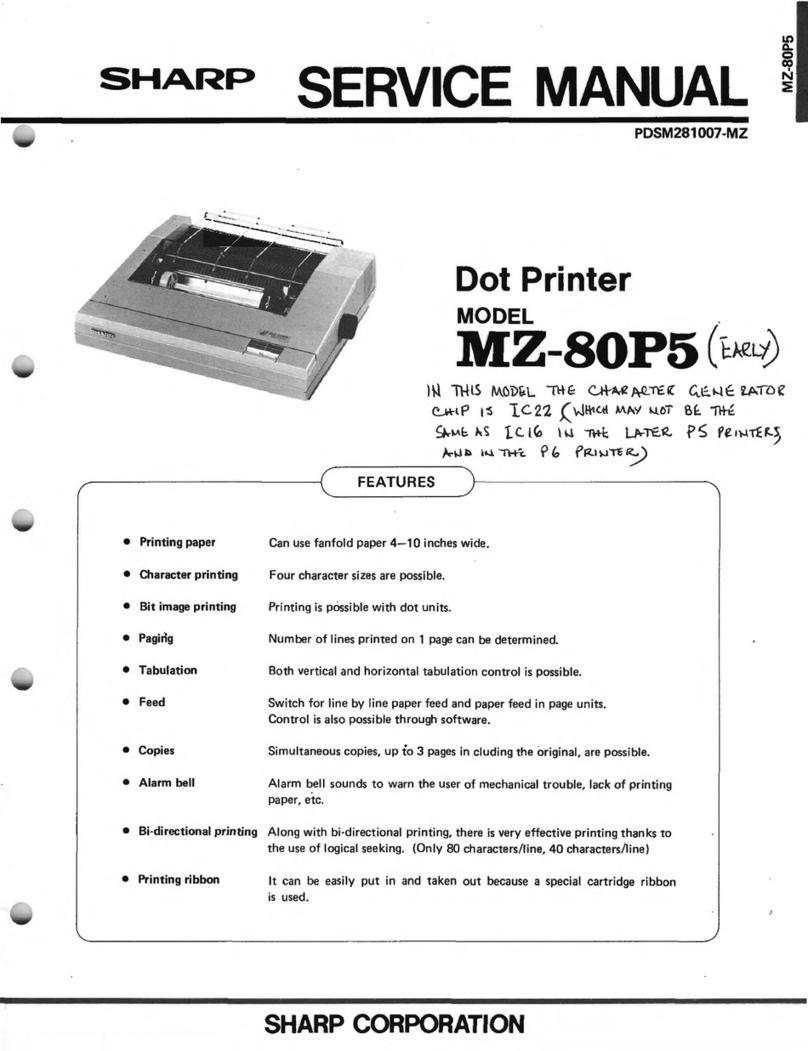
Sharp CE-129P User manual

CODE:OOZCE129PSM/E
-
CE-l29P
SERVICE MANUAL
SHARP
1. PRODUCTS OUTLINE
The CE-129P printer is an optional printer with the cassette
interface designed for use with the pocket computer models
EL-5500, PC-1401 (EL-55001I). PC-1402, PC-1421 (EL-
5510), and PC-1430 (EL-5400)
2. WCIFICATIONS
Printer type: Oot matrix thermal printer
(MTP-201), identical to the one
used for the CE-125
Printing digit:
Printing speed: 24 digits/line
Approx. 0.8 line/second
(Printing speed varies with the
number of printing digits per
line.]
Approx. 0.8 line/second
Thermal paper (heat sensitive
paper), EA-1250P
18mm (23/32")
roll outer diameter (max.)
58mm (2-9/32") wide
6V:::
(OC):
Heavy duty manganese battery,
size
AA
(or
RG)
x 4
AC:
local voltage with AC adaptor
EA-23E (Option)
Heavy duty manganese battery,
size
AA
(or
R6,:
Approx. 3,000 lines
UM-3: Approx. 2,000 lines
(Condition: 555555555555. is on
continuous printing at an operat-
ing temperature of
lOD
C, this
number of printing lines varies
with the type of battery or the
way of use.1
3.0W
OD
C -
40D
C (32°F -l04
D
F,
198(W)
x
156(0)
x
34(H)mm
7-25/32"(W) x
6-5132"(0)
x
1-11/32"(H)
385g (0.85Ibs_1 (with batteries)
Hard case,
Dry
battery )( 4, Paper
roll x 3, Cassette cable, and
Operation manual
Paper feed speed:
Paper:
Power source:
Operation:
Power
consumption:
Operating temperature:
Dimensions:
Weight:
Accessories:
MODEL CE-129P
• Printer/Cassette Interface .
3. TAPE RECORDER INTERFACING
METHOD
CE·I29P Tape recorder
Tepe R~order CE·129P
I••
;1!tI
I I I
I@!!!..
Grey
ptug
(tr.nsftr
.nd
eDU.liDnl
+-BI .. kplug
bemoll
contral)
-- kpl...
I ..
=<>troll
Grey
pI...
---+
!transfer
and
ClDUalionl
Red
plug
(racordingl
i
c.sette
connec:tion
cable
Cassette Tape Recorder
The following is a description of the minimum tape
recor-
der specifications
necessary
for interfacing with the CE-
129P.
!lem Requirements
1. Recorder Type Any t&perecorder, standard cassene
or micrCH:8ssette recorder, may
be
used in accordance with the re-
quiremenu outlined below.
2. Input Jack The recorder should have a mini-
jack input labeled "MIC". Never
use the "AUX" jack.
3. Input lmepedance The input jack should
be
a low
impedance
input (200 - 1,000
OHM.)
4_Minimum Input Level Below 3mV or
-50
dB.
5. Output jack Should be a minijack labeled "EXT.
(EXTemal speaker)", "MONITOR",
"EAR (EAR-phone)" or quivalent.
6. Output impedance Should
be
below 10 OHM.
7. Output level Should be above 1V (practical rnax-
imum output above 100 mW)
8. Distortion Should
be
within 15% within a
range of 2 kHz through 4 kHz.
9. Wow and Flutter 0.3% maximum (W.R.M.SI
10. Other Recorder motor should not fluctu-
ate
speed.
------
SHARP CORPORATION
Do not sale !

-
CE-l29P
NOTES:
• Some of tape recorders may not operate properly owing
to different specification or electrical characteristies
affected by signal distortion, electrical noise, leveldrop-
out caused after long years of use.
• When using the tape recorder fitted with the mixing
feature, it needs to disable the mixing function for both
recording and playback_
• Oepending on the
tape
recorder used, better reading
result may be attained when the red plug is unplugged
from the MIC[ack,
• As it may impede proper data transfer and verification
depending on the position of the volume control, tone
control, bass control, and treble control, try to find the
optlrnum
levelby varying their positions.
4. CIRCUIT DESCRIPTION
The CE-129P has two microprocessors; the P-CPU (inside
of CE-129P) by with data transfer is carried out with the
host CPU (M-CPU: inside of computer) and the prlnter
control PCU.
I
M-CPU to P-CPU data transfer method
Since there are no SEl1 and SEl2 used for the PC-1401
and El5500, OEVICE SElECT is dependent on the
contents of data.
(UEVICE SELECTJ
DOUT
(11
For OEVICE SElECT, XOUT becomes high.
(2) As the P-CPU receives a high state of XOUT, it sends
ACK to the M-CPU.
(3) As the M-CPUreceivesACK, it sends back BUSY.
(4) Oata is received to the P-CPU with a high state of
BUSY. ACl, REMOTE ON, CPU select actions is
carried out depending on the contents of data.
[print data transfer
I
(DATA
DAHSPORTATlorrn
XOUT
IUSY ~
ACK / \
~IIIY ••
(1) XOUT goes low when the print data istransferred.
(2) BUSYfrom the M-CPUturns high level.
(3) Upon receipt of BUSY, ACK of the P-CPUis set high
and the data is received to the P-CPU.
Since the data is transferred in bit by bit serial mode, above
steps (2) and (3) are repeated eight times to complete
transfer of one data, For instance, those steps are repeated
for 192 times (24 x 8) in order to transfer a 24 digits data.
The print commands, however, is sent out to the P-CPUat
the end of the data in a form of the code "00".
5. BLOCK DIAGRAM
lfToulZ
I~EM.OTEI
I
EAR CIl"CU
it
XiD
"&'
~
r-I
Low
battery
J
Xoal -"'" IIIC
-
P21
P&3
PI2 P23
BuS)"
PlI
Ooul Pli CPU
P22
DiD PSI P20
ACK P62 P50
POO P03
P53
SELI
,I
SELZ
DI.... RIW
JIJSY
sn
I
HI-1
IDF PCU
T
TI
I
PD
R
Drivrr I. C
Z~ro-
Crn.
I.C
HI-1
11
T
PRINTER
-2-
Do not sale !

-
CE-l29P
6.
P-CPU
(MPD75060515, 516 SIGNAL DESCRIPTION)
C-MOS 1 chip 4 bit micro-computer
Terminal Terminal Signal name Input/Output Description
No. name
1NC
--
2 NC
-
-
3CL1
-
-
System clock Oscillation frequency -- approx. 200 KHz
4NC
- -
5CL2
- -
System clock
6NC
-
-
7 GNO GNO
-
Power supply, OV
8 RST
-
Input P~U reset input: when power supply is ON, reset operation.
Min 30
JlS
9P10 VOO Input/(Output) Setting VOO
(-4""
-6V)
10 P11 OOUT Input/ (OutpUt) Oevice select data and print data
_1
P12 XOUT Input/(Output) ldentification of the contents of OOUT (whether it is device select
data or print data.)
12 NC
--
-- .... .... ....
15 NC
-
-
16 P13 8USY Input/(Output) Handshake signal. latch si!Jlal by which the P-CPU abtains OOUT
data.
17 P50 01 Input/Output Oata bus line between the P-CPU and the PCU.
18 P51 02 Input/OutpUt Data bus line between the P-CPU and the PCU.
19 NC
-
-
20 NC
-
-
21 P52 03 Input/Output Oata bus line between the P-CPU and the PCU.
22 P53 04 Input/Output Oata bus line between the P-CPU and the PCU.
23 POO SEL1 Input Select input signal. It is not
used
in the PC-1400, El-5500 series.
24 P40 VOO Input/Output Setting VOO
(-4-
-6V).
25 NC
-
-
-
-
.... ....
28 NC
-
-
29 "- P41
l.B
Input/(Output) low battery detection signal. Normal high.
~~ P42 VOO Input/(Output) Setting VOO
(-4....
-SV).
VOO VOO
-
Power supply VOO
(-4....
-6V)
32 NC
-
-
33 GNO GNO
-
Power supply OV
34 P43 GNO Input/Output Setting GNO (OV)
35 NC
-
-
36 X2 NOTUSE
-
37 NC
-
-
-
.... .... ....
40 NC
-
-
41
POl
SEL2 Input Select Input signal. It is not used in the PC-1400, EL-5500 series.
42 P20 R/W Output Read/write signal for the PCU. High: read High-low: write
43 P21 REM2 Output Remove OFF pulse signal
44 P22 (SEL2) Output PCU chip select signal. High: selected, low: non select
45 P23 (SEl1) Outpl.'t PCU clear signal. High: ACl active Low: normal
46 Ne
--
47 P60 JN (lnput)/Output Paper feed key strobe signal when CPU: MP07506G516 is used.
48 P61 OIN
(I
nput)/Output Printe Error signal to host CPU. High: printer Error. low: Normal
49 P62 ACK
(I
nput)/Output Handshake signal P-CPU to host CPU.
50 P63 REMl (lnput/Output Remoto ON pulse signal.
51 NC
- -
52 NC
--
-8-
Do not sale !

-
CE-l29P
7. PCU (SC6994) SIGNAL DESCRIPTION -
Pin No. Signal Name In/Out Oescription
1SEL2 In Select
2SEl1 In Select
3 VOO Out Power supply
4ACl Notused
5
BUSY In Histl:
chip
select - - - - - - - - - Low: Non~lect
I
,
6
RIW
In Hi!#l:
read
Hi!#l to low transition: write
7-10 04-1 In
Dm
input
11 STP Notused
12 S In
Dm
transfer mode select Une
Hi!#l: serial input - - - - - - - - low: parallel input/output
13 24 In Print digit select Une
Hi!#l: 24 digits (GNO connected) Low: 16 digits
14 10F Out Printer motor drive signal
15 H7 Out Printhead element on pulse
16 H6 Out Printhead element on pulse
17 GNO In Power supply
18-22 H5-H1 Out Printhead element on pulse
23
R
In Printer reset (printhead home position detect)
24 PD Out Power down (in supply during printer operating cycle, otherwise,
power is not supplied to the printer drive circuit.
25 T In Printer timing (generated from the tachogenerator of the motor)
26-28 TSl-3 In Test pins
29 VP1 Out Printer control circuit supply power
30-32 BCl-3 ln/Out
PCU
frequency controI
33 CCK Out Clock test pin
34
l:fA
In
I
(Print density adjust pin._.JA and JB pin connection
,
Notused
I
35 HB
I
36 HC In varies according to the printhead rank).
37,38 Cl1,2 In Basic clock pulse control resistor fitting pin
39
PF In Paper feed key input
40 NP In GNO Connected
41 ACL In All elear input
42 OP3 Out ACl select (high when on)
43 OP2 Not used.
44 OPl Notused.
8. SERVICE CAUTIONS
I
Cautions in exchanging the printer unit
I
In order 10 prevent print density variation causecl by
thermal head resistance variation, the printhead is classified
into three ranks of A, B, and C, and the rank is indicated
on the reverse side of the printer u~it F.P .C. After exchange
of the printer unit, relevant circuit change must be observed
in accordance with the procedure mentioned below.
Leave all open when the rank B printer is used.
Short JA when the rank A printer is used.
Shrt JC when the rank C printer is used.
Table·1
-4-
Do not sale !

Rankirw (A,BorC)
t
roz-ara
PRINTER UNIT
<
Printer head ranking position>
After the above procedure, adjust by means of the 22-
Kohms protentiometer so that an optimum print quality is
obtalned. The circuit has been so designed as to attain the
best result with the potentiometer
set
at
its midway_
Therefore, existence of aremarkable print density variation
might involve the following problems:
1.A>p in head performance
2_~ality change in the termal recording paper
3.
Throuble in the thermal control circuit
1. When VR density Idjustment
is
needed
A) After replacement has been made in same electronic
component parts inside the solid line.
B) When service request is placed from the user claiming
that print density is too low or high.
2. Print density control method
• Before the print density adjustment, make sure that the
jumper pad is properly connected in a manner
as des-
cribed in Table-1.
• The VR should necessarily be set to the position
mentioned in Fig. 1. If set too much counterciockwise,
it may damage the printhead which mayaiso cause dot
omission.
~VR
"-.J
FiS_'
. - 5-
• Ensure before the operation of the oscilloscope that the
time axle control knob is set at CALIBRATION.
Adjust the print density in the fOllowing sequence, step 1
thru step 5.
Step 1.
Short the TEST3 jumper pad with a soldering.
t669:>S
,-,~
'1iiOn,
_.- I
'LJ!I,
Solder and sho"
thispo"ion
Fig.2
Step 2_
Connect the EA-23E AC adaptor with the CE-129P after
the TEST3 pad temperature came down to the room
temperature, and check the voltage between the JT pad
and
#9
pin of the lB1256 (Vp) using the voltmeter.
(Vp: check)
..
~
I-
..
0
2
a:
w
11..
W
~
:)
11..
11
(,
~
11
a
•
Step 3. StE
While observin9 a pulse waveform on the oscilloscope
came from the CLOCK CHECK terminal, adjust the
22Kohms VR so that the pulse period (T) should
become the value shown in the graph below.
t669:>S
• Pulse waveform
Fig. '3
StE
@
1. C
c
o
2. S
li
3. ~
C
u
~
1. C
2. S
li
3. S
1.
Do not sale !

aa" ._... .._.
---
~-
'--'
......
-
---r--t- ....-_...
i
!
(An adjustment example)
When Vp is 6.2V under the room temperature of lO°C.
It
should
be
adjusted to T
=
17.3µS, according to the
above graph.
• In case the frequency counter is used
Frequency counter may
be
used instead of the
oscilloscope. In this case, connect the frequency
counter to the CLOCK CHECK terminal and adjust
the VR so that 'it should be the frequency range
shown in the above graph.
Step 4.
Have the printer worked to check the aetual print
density. Among other things, let the capital
"I"
printed
and ensure that there is no vertical dot omission.
Step 5.
After the check of the print result, remove the solder
oAe TESTJ terminal (Step (1)) aod replace the
ca.et back in the unit with care not to seize any lead
wire with the cabinet.
I
CE·129P OFF CURRENT CHECK
I
t ,
Operate the paper feed key when a computer is not
connected to the CE-129P, and check if paper feed
operation (ON,.OFF) isexecuted normally.
2. Supply -5.0V from stabilized
oe
power supply to Vp
fine. (GND
=
OV:standard).
3. Measurethe current on Vp line when the power switch is
OFF. If it is 20µA or less, it may
be
recognized !hat the
used power while the power supply is OFF is normal.
I
Current check during. printing
I .
t.
Connect a computer to the CE-129P circuit.
2. Supply -5.0V from stabilized
oe
power supply tp Vp
line. (GND =OV;standard).
3. Set the power switches in the computer and the CE-
129P to ON to execute check program 1.
(IDEE
[Ä))
N
::z::
..
~
>
o
z
w
~
o
w
a:
u.
-6-
-
CE-l29P
- Print sampIe -
444444444444444444444444
444444444444444444444444
444444444444444444444444
444444444444444444444444
444444444444444444444444
- Check.program 1 -
100:·A
Y
FOR 1=1 TO 5
110:LPRINT 9444444'44444
444444444444"
120:NEXT I
130:.END
4. Measure the current on the Vp line in printing, if it is
SOOmA or less,
it
may
be
recognized that the used
power during printing is normal.
I
Low battery detection circuit
I
A circuit constant is defined so that low battery detec-
tion may
be
executed when Vp voltage is -3.8V or less.
When checkprogram is executed after applying -3_8V to
the Vp line, if display of ERROR 8 appears on the eom-
puter display without printer operation, it may be
reC09nized that the low battery detection circuit is
narmal.
I
Chraetar printing grade check
I
Check the printing grade by executing the check pro-
gram 2. (~ IJ) .
- Print sampie -
!YU$%&'()*+,-./012345678
9:;(=)?@ABCDEFGHIJKLMNOP
QRSTUYWXVZ[~]"-
- Oleck.program 2 -
200:
Y
:8"
210:LPRIHT Y!Y;CHRS
34;Y
U$%&Y;CHR$ 39;Y()*+,
-./012345678
Y
220:LPRINT Y9:;(=)?@ABCD
EFGH I .JKU1HOP
Y
230:LPRIHT YQRSTUVWXYZ
Y;
CHRf 91;CHRf 92;CHR$
93;""";CHR$
95
240:END
Do not sale !

..
-
CE-l29P
9. CIRCUIT DIAGRAM
•
l_
_L
l_
~
·
..
..
%
~
,
..!.
D..
e
:>
-
äl"
~I
...,
-
w'·
-
r-
'It
'-
r-
r-
1
1
r
I>
~
,~~ - L
CI
~
-
N
..
~
N
N
N
..
~
@
N
>
10
I
""
,
.~
0
>
..
• >
..
'i::l
o
D.
!:u
uv
Ö
e
CI>
er
-
E"
~ ID
.-
·
.,
i:i! ~~t~I
t
Ilr
I'"
J
ID
------r
u
CD
r-
Do not sale !

I
I
""'"
:oe •
xc;
I'-
-
111
-
"$
10
Jl
""""r"
Z
~
.a:
LL.>-
8
O-~
o
-t;-
..
;:;:
~
u
N
>C
"'"
0-
N
~
I'-
N
!XI
a,lI)
(\I
Ö
,
..:
E
"'
GI
l/)
er ~
-
L
I
I
,:/1
I I III II
1
.><
-
I
t~t-
JMt.
--0
>
S
c
z
>
\!)
..0
I ~
<1..., : •
.-!-
SI ,
0
O~
> ..
:8 '..-'
N
)(
"'"
2
N
-
E"
~ 10
.-
•. 10
;:.f
1
L....;.
.6-:,;
...
• >
..
';;:,
o
CL
!:U
U'-J
CI)
I
""
I
UI
1
r
-8-
x
._
t-
u
t-
ID
Do not sale !

10. MAIN P.W.B
I! ~ • , ,
!
.1
'1
1
!!
~
!~
10 '"
;; :ä
ci ci
z z
~
$ $
'"
~g
...
0
z ,_
........
Do not sale !

-
CE-l29P
Do not sale !

-
CE-l29P
11. SUB P.W.B
I
:;
..
i'n
.. 111
...
....
.....
Ir:
•
-11-
Do not sale !

12. PARTS LIST
&
GUIDE
l"
"'-1
eJ,
31
I
~~ I
A
32
\3
/
..
_____ -12'~.•..._..... _
Do not sale !

SHARP CORPORATION
Information Systems Group
Quality &Reliability Control Center
Yamatokoriyama, Nara 639-11, Japan
1985 August Printed in Japan®
-
CE-l29P
[2J
Main PWB unit
NO. PARTS CODE PRICE NEW PART DESCRIPTION
I
RANK MARK RANK
I
35 VRS TP2BD224J AA CResistor O/8W 220KO +5~)
36 VRS-TP2BD332J AA CResistor U/SW 3.3KO + 5~)
I
37 VRS-TP2BD470J AA CResistor (l/SW 470 +~
38
VRS-TP2BD471J AA C Resistor (l/SW 4700 +~
39 VRS TP2BD472J AA CResistor (l/SW 4.7KO +5~)
40 VRS TP2BD473J AA C Resistor (l/SW 47KO + ~
41 VRS TP2BD474J AA C Resistor (1/SW 470KO +~
42 VRS-TP2BD563J AA C Resistor U/SW 56KO + 5~)
CUnit)
901 OUNTK8655CCII BG N E Main PWB unit
[3] Sub PWB unit
NO. PARTS CODE PRICE NEW PART DESCRIPTION

RANK MARK RANK
1 QCNCM1307CCIB AK B Connector Cll pin)
20JAKCI003CCII AD B Jack (tor AC adaetcr)
3 QJAKCI013CCIZ AC BJack (for MIC)
40JAKCI016CCZI "C CJack socket (for Remote)
50S W- S 0 0 7 5 F C Z Z AF B Slide switch
6 QSW S1255CCZI AG B Slide switch I
7 QTANS1408CCZZ AB CSpring
I
8 VCTYPU1NX104M AB C Capacitor U2WV 0.10"f)
I
9 RF i lNIOO8CCZI AH C Filter (ESD-H-14B)
10 RRlYZ2400QCZZ AP B Relav
II
VCEAGUIAW107M AB CCapacitor_(lOWV l00uF)
12 VCEAGU1AW108M AC C Capacitor (lOWV l000~
13 VCTYPUIEX472M AA C Capacitor (25WV 4700pf)
14 VHDDS1588l2 1 AB BDiode (DSI588l2)
15 VHD10EIN/// 1 AB B Diode (lOEIN)
16 VHEHZ7A3/// 1 AB B Zener diode (HZ7A3)
17 VRD ST2EY391J AA CResistor (l/4W 3900 +5~)
18 VRD ST2EY681J AA C Resistor {1/4W 6800 +5%l
19 VRD ST2EY682J AA CResistor (l/2W 6.SKO +~~
20
VS2SA937 R/ 1 AC B Transistor_{2SA937 R_l
21 VS2SC1826 GBC AF B Transistor {2SC1S26 GBG!
(Unitl
901_ DUN T K 8 6 5
~~l I
BG N E Sub PWB unit
----
{II Packing material & Accessories
NO. PARTS CODE PRICE NEW PART DESCRIPTION
RANK MARK RANK
1PHOG 1093CCZI AB C Rubber cap for llpin connector cable
2 QPlGJ1022CCZZ AQ CCassette cable
3 TCAUKl198CCII AA CCaution card for 11pin connector rubber cap (Export)
4 UBAGC1438CCZZ AU N D Carrving_ case

5 TiNSE4456CCZI Al N D Instruction book_{USA onlv)
Ti NSM4478CCIZ AV N D Instruction book
_{E,
Fjil S)
6 SPAKA517ACCZZ AF N D Packing cushion for set
7 SPAKC518ACCII AH N D Packing case (USA only)
SPAKC519ACCZZ AH N D Packillg case (Except USA_l
8 TlABPIOO2ECZZ AB N CBar cord label (USA only)
11 -
J
BLO SGO ~ 1
73638-105 S/NCEI29P
.
.
.
'..
.."
-
.
~
".
------------------------------
JI6 - 141085/106002000
-14-
Do not sale !

..
rn
Exteriors
-
CE-l29P
ihield tape_
GCOVA
NO.1 PARTS CODE
IBatterv cover
1Batterv terminal
(Ef:j)
PRICE
I
NEW
RANK MARK
AC IN
Q__
I
Paper cover
PART
RANK
I DES C R IP T ION
A
D
I
Paper cutter
HD
PCUT-
B
'rinter cushion
AD
I
ND
I
Dec.
panefX
N
PCUSS
AC
I
N
o
I
Dec.
panel
B
lnsulator
_!_I
K
i-I
_N
o
I
Top cabinet
rhermal printer unit CMTP-201)
o
ilide switch spacer
_!
BG_I_N icrew (2X5)
iub PWB unit
131 QCNW-_l
14
I
QTANZ
1
4__
2_6_C C_Z Z
_Ui]_l_K-N-B-Z I 808
ec
0 I
AD
I
NFPC (APllL08SAOS)
16
I
L
FiX
I 1 4 7 C
C
Z Z
AB
e
I
Terminal
C
J
Fixing plate tor P.F key top
AG D
I
Key top (P.F)
17TXussoTif PO
4
000
AA
AA e
I
Screw
(2
X4)
C
B
'OIQJAKCI lack (tor AC adaptor)
18 QCNW=132 8 CC Z Z-
19 QCNCMI307CCIB
~ __ji
AK
AK lack socket (tor Remote)
eezz
D
~2 AK ,ck (tor MIC)
~310SW-
N
B
I
Paper feee! switch
lide switc
lide switcl
lain PWB unit
Z7l_Q~ __ K I 2 AD
P
~ubber foot
~atterv terminal
(e)
C
AB
I
N
nsulator sheet
PS ihield plateN
Nlottom cabinet
'ape
~f>_LOll
UBSF26P
~ I
Q
T A__1I_l I
I)
S ~
151
Q
TA
N Z I 5_0 6
161
Q
T A N Z I I 8 6
C
17
I
Q
T A N Z I
5 0 5 C C
Z
Z
18
I
G F T A~ 2 1 C C Z Z
IBatterv terminal B
IBatterv terminal
..Lr--:_N_
AA
icrew
C2.6X6)
AA
I
1!
AC
I
_N
[ll
Main
PWB
unit
NQI PARTS CODE DESCRIPTION
I PSPAPI230CCZZ
_2_
Q
C N ~
w
i
3 0 8 C C A
i
'JQulrlnter (8_pin plack)
3IQSW-K I n-5CCll
RC-CZI021CCZZ
RC-CZI03ICCZZ
RC-CZI035CCZZ
Dt'_"'7In~IIt't'77
~_p_1 _
-1-B
1~_l _I
i
1
Spacer
[PJlpeI' Jeee! switch
A
:apacitor CI 1lF)
. (lOOOpF)
:J.!.QQ2
;apaCllor (470p
. (1S0pF)
ICCZ
---Z
_81
RC-I
RC-'
"ol_j
:-~
r=i
AC
I I
C
1
Capacitor
(iowv
3.31lFf
liode (DAP202)
'-
I-I liode (DAN202)
1-'
ransistor
ransistor (2o:::
n1
1-'
·ransistor (2SA 1179)
I-I 'ariable resistor (22KO)
1-
ransistor (?o:::~?
1-
//-
liode (IS
liode (DS
//-
;-5 I
HiLBI256//-
:ener diode (HZ3BLL)
(D7S06G-515)
(LBI2SIll_
_!!_i
M 5 1 2 3 L / /-
141 V H
i
S-C 6 9 9 4//-
lJC _
(M5123L
__C____j
Resistor U/BW lKO
±5%'
__C____j
Resistor Ül8W 10KO -± 5%)
VRS-TP~JlDI02
V R S-_I_F>_2 BO I
0_3
..Y_RS-TP2BD_104 C ~istor (1/8W lOOKO ±5%)
VRS-_I_F>_2BDI0i
_Y_R S-T P-2 B D_I 24
3OIVRS-T_!>_2BDlli
AAl
I
C
--I
Resistor U/8W I.OMO ±5~
.Po
A
I I ~_
I
Resistor U/8W 120KO ±2%)
AAl
I
C 'Resistor U/8W 15KO ±2%'
lil_Y_R s-t-P 2 B D_1_
12IVRS-T_!>_2BD2
33IVRS-TP2BD2
AAl
I
C , ~istor Cl/8W 20KO ±2%r
_A_!_j_
I_j:
I
ResistorH/fJW..2.2KO ±5%)
AAl
IC
LResistor O/BW 22KO ±_5%1_
_34
I
V__ftJi - T P
2
B
P_1_
AAl I C
I
Resistor Cl/BW 220KO ±2%'
-13-
Do not sale !
Table of contents
Other Sharp Printer manuals

Sharp
Sharp MX-B427PW User manual

Sharp
Sharp CE-515P User manual

Sharp
Sharp AJ-1100 Setup guide

Sharp
Sharp DP-750 User manual

Sharp
Sharp MX-C382SC User manual

Sharp
Sharp AR-200M User manual

Sharp
Sharp AR-M351N User manual

Sharp
Sharp AR-M550N Service manual

Sharp
Sharp AR-CF2 User manual

Sharp
Sharp JX-9460 User manual

Sharp
Sharp CE-140P User manual

Sharp
Sharp MZ-80P4 User manual

Sharp
Sharp AR-122E N User manual

Sharp
Sharp BP-50M26 User manual

Sharp
Sharp MZ-1P16 User manual

Sharp
Sharp MX-B400P Installation and operating manual

Sharp
Sharp AR-350 User manual

Sharp
Sharp JX-9500E User manual

Sharp
Sharp AR-M350 Imager User manual

Sharp
Sharp Network Scanner User manual