Siemens SXG75 Setup guide

Release 1.0
Technical Documentation 01/2006
TD_Repair_L3_SXG75_R1.0.pdf Page 1 of 73
Service Repair Documentation
Level 3 – SXG75
Release Date Department Notes to change
1.0 24.01.2006 BenQ Mobile CC S CES New document
Company Confidential
2006©BenQ

Release 1.0
Technical Documentation 01/2006
TD_Repair_L3_SXG75_R1.0.pdf Page 2 of 73
Table of contents:
1Instruction..................................................................................................................................4
2List of available spare parts.....................................................................................................5
3Required equipment for level 3................................................................................................7
4Required software for level 3 ...................................................................................................7
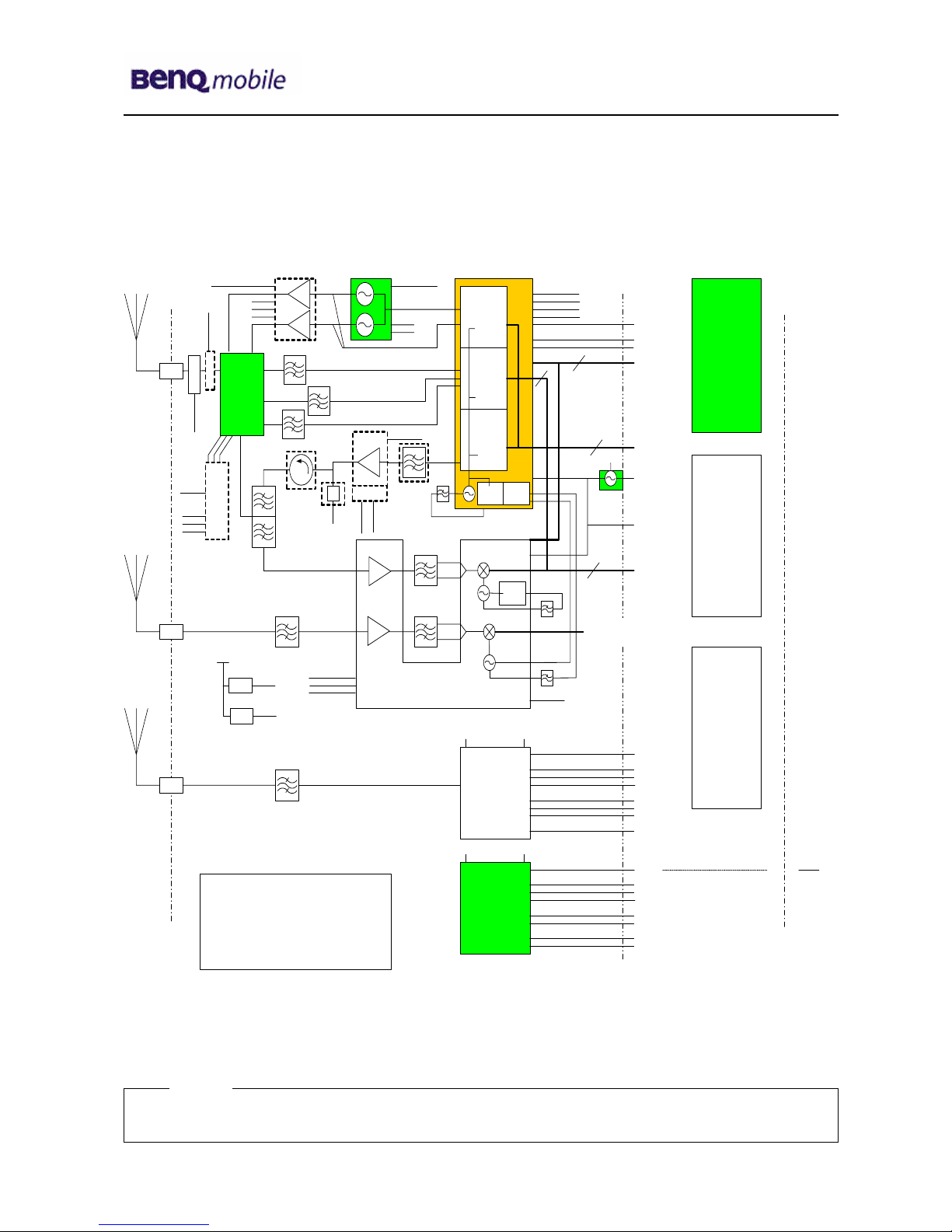
5Radio part...................................................................................................................................8
5.1 BLOCK DIAGRAM RF PART.......................................................................................................9
5.2 RECEIVER (RTR6250 AND RFR6250)...................................................................................10
5.3 TRANSMITTER.......................................................................................................................12
5.4 ANTENNA SWITCH .................................................................................................................15
6Baseband .................................................................................................................................17
6.1 BLOCK DIAGRAM ...................................................................................................................17
6.2 MSM6250 PROCESSOR ........................................................................................................18
6.3 MSM6250 INTERFACES ........................................................................................................23
7FM Radio ..................................................................................................................................32
7.1 FM RADIO INTERFACE ...........................................................................................................32
8Power management ................................................................................................................34
8.1 PM6650 FUNCTIONAL OVERVIEW ..........................................................................................34
8.2 VOLTAGE REGULATORS AND VOLTAGE CONVERTERS .............................................................36
8.3 ADDITIONAL POWER SUPPLIES...............................................................................................38
8.4 PM6650 SIGNAL INTERFACES ...............................................................................................38
8.5 POWER ON/OFF SEQUENCING...............................................................................................40
9Battery/Charging .....................................................................................................................43
9.1 BATTERY ..............................................................................................................................43
9.2 PHONE SHUTDOWN DUE TO LOW BATTERY .............................................................................43
9.3 CHARGING............................................................................................................................44
10 Audio interference and suspension of pulse charging .......................................................50
11 MMI ...........................................................................................................................................50
11.1 DISPLAY ...............................................................................................................................50
11.2 KEYPAD................................................................................................................................54
12 Acoustics .................................................................................................................................58
12.1 MICROPHONE,SPEAKER AND HANDS-FREE SPEAKER..............................................................59
12.2 AUDIO ACCESSORIES ............................................................................................................59
Company Confidential
2006©BenQ

Release 1.0
Technical Documentation 01/2006
TD_Repair_L3_SXG75_R1.0.pdf Page 3 of 73
13 Cameras ...................................................................................................................................59
13.1 2MPIX CAMERA.....................................................................................................................59
13.2 CIF CAMERA.........................................................................................................................60
13.3 CAMERA BUS INTERFACE ......................................................................................................60
13.4 CAMERA FLASH TRIGGER ......................................................................................................60
14 Vibramotor ...............................................................................................................................62
15 IrDA and fuel gauge ................................................................................................................63
15.1 IRDA TRANSCEIVER ..............................................................................................................63
15.2 BATTERY FUEL GAUGE AND IRDA MULTIPLEXING....................................................................63
16 Accessory interface ................................................................................................................66
16.1 OVERVIEW............................................................................................................................66
16.2 UART AND USB MULTIPLEXING ............................................................................................67
16.3 CONNECTOR DEFAULT CONFIGURATION.................................................................................68
16.4 ACCESSORY DETECTION .......................................................................................................68
17 UART ........................................................................................................................................69
18 USB...........................................................................................................................................69
19 SIM Interface............................................................................................................................70
20 MMC interface..........................................................................................................................71
21 Component placement............................................................................................................72
Company Confidential
2006©BenQ

Release 1.0
Technical Documentation 01/2006
TD_Repair_L3_SXG75_R1.0.pdf Page 4 of 73
1 Instruction
This Service Repair Documentation is intended to carry out repairs on BenQ Mobile repair level 3.
The described failures shall be repaired in BenQ Mobile authorized local workshops only.
All repairs has to be carried out in an ESD protected environment and with ESD protected
equipment/tools. For all activities the international ESD regulations has to be considered.
Assembling/disassembling has to be done according to the latest SXG75 Level 2 repair
documentation. It has to be ensured that each repaired mobile phone is checked according to the
latest released General Test Instruction document (both documents are available in the technical
support section of the C-market).
Check at least weekly C-market for updates and consider all SXG75 related Customer Care
Information and Repair Information which are relevant for the SXG75.
SXG75 partnumber on IMEI label: S30880-S8900-#xxx
, while # can be any letter (A-Z) and xxx can be any number from 100, 101, 102....
Scrap handling: All scrap informations given in this manual are related to the
SCRAP-Rules and instructions.
Attention: Consider the new "LEAD-FREE" soldering rules
(available in the communication market) and avoid excessive heat.
If you do have any questions regarding the repair procedures or spare parts do not hesitate to
contact our technical support team in Kamp-Lintfort, Germany:
Tel.: +49 2842 95 4666
Fax: +49 2842 95 4302
Company Confidential
2006©BenQ

Release 1.0
Technical Documentation 01/2006
TD_Repair_L3_SXG75_R1.0.pdf Page 5 of 73
2 List of available spare parts
(according to Component Matrix V1.03 - check C-market for updates)
Com
p
onent Ordernumbe
r
Descri
p
tion
V101 L50640-D4060-D670 DISDIODE DUAL ESD-PROTECTION SOT23
V200 L50630-C1101-D670 DISTRANS SI1555DL
N200 L50645-K280-Y337 IC FEM LMSP43MA-288TEMP GSM UMTS SMD
Z203 L50645-K280-Y323 FILTER DUPLEX WCDMA
Z200 L50645-K280-Y331 FILT SAW RX PCS1900MHZ B7846
Z201 L50645-K280-Y332 FILT SAW RX DCS1800MHZ B7844
Z202 L50645-K280-Y333 FILT SAW RX GSM900MHZ B7837
D500 L50620-L6165-D670 IC TELEC TRANSCIEVER RTR6250 QFN56
N300 Not defined yet IC MODUL PA PF0814 (PA-Type3) PB Free
V300 L50630-C1101-D670 DISTRANS SI1555DL
Z300 L50645-G100-Y108 OSCOSCI TXVCO 824-1910MHZ SMD
Z400 L50645-K260-Y93 ISOLATOR 1920MHZ-1980MHZ SMD
D400 L50651-Z2002-A66 IC TELEC ACPM-7881 SMD
V400 L50630-C1101-D670 DISTRANS SI1555DL
Z402 L50697-F5005-F88 IC TELEC RF-DETECTOR SOT23-6L
Z401 L50645-K280-Y314 FILT SAW UMTS2100 1950MHZ B7754
Z602 L50697-F5020-F34 EPCOS SAW LOW-LOSS-FILTER 2140,0MHZ LG02
X600 L36334-Z97-C334 CONNECTOR COAX SOCKET SWITCHED
Z600 L50645-K280-Y293 FILTER SAW AGPS 1575,42MHZ B7840 SMD
Z601 L50645-K280-Y304 FILSAW 1575,42 MHZ B7829 SMD
N600 L50620-L6166-D670 IC TELEC RECEIVER GPS UMTS RFR6250 QFN48
N700 L50610-U6197-D670 IC ANA STEREO-AMPLIFIER TS4975 CSP12
D800 L50620-L6164-D670 IC TELEC MSM6250 CSP409
Z1000 L50645-G200-Y27 OSCOSCI VCTCXO 19.2MHZ SMD
V1100 L50640-C3008-D670 DISTRANS PNP 0,5A 30V SOT89
V1102 L50630-C3007-D670 DISTRANS P-CH SI2333DS FDN306P SOT23
N1100 L50610-C6181-D670 IC VOLTAGE REG.TPS73601DRBR SMD ADJUSTA
V1101 L50640-D5086-D670 DISDIODE RB551V-30 PMEG3005AEA SOD323
Z1200 L50640-U6064-D670 FILTER EMI (Fi-Type7) PB Free
Z1201 L50610-C6179-D670 IC SPDT SWITCH DUAL MAX4717EBC+T UCSP12
V1303 L50640-D4043-D670 DIODENARRAY ESDA6V
Z1300 L50645-F102-Y42 OSCCRYST 32,768KHZ 7,0PF 30PPM SMD LF
N1300 L50645-J4681-Y57 IC POWER-MANAGMENT PM6650
V1301 L50640-D5086-D670 DISDIODE RB551V-30 PMEG3005AEA SOD323
D1300 L50610-C6183-D670 IC LOGIC NAND 74LVC1G00 SOT886
V1302 L50640-D5086-D670 DISDIODE RB551V-30 PMEG3005AEA SOD323
V1300 L36840-D5076-D670 DIODE SOD323 (Di-Type7)
Z1600 L50645-K280-Y328 FIL BP 2,4GHZ SMD
N1600 L50610-L6155-D670 IC TRANSCEIVER BLUETOOTH BCM2004 SMD
D1800 L50620-L6150-D670 IC TELEC TEA5764HN
V1800 L36840-D61-D670 DIODE 1SV305 (Di-Type4)
Company Confidential
2006©BenQ

Release 1.0
Technical Documentation 01/2006
TD_Repair_L3_SXG75_R1.0.pdf Page 6 of 73
V1801 L36840-D61-D670 DIODE 1SV305 (Di-Type4)
V1900 L36840-C4057-D670 TRANSISTOR EMD12 EMT6 (Tra-Type8)
N1900 L50610-C6152-D670 IC ANA REG 2*2,85V 150MA USMD8 LP3986T
D1900 L50610-B6198-D670 IC LOGIC BUFFER 74ALVC16244AZQLR VBGA LF
D1901 L50610-B6198-D670 IC LOGIC BUFFER 74ALVC16244AZQLR VBGA LF
V2000 L36840-C4014-D670 TRANSISTOR BC847BS BC846S (Tra-Type7)
D2100 L50610-B6134-D670 IC LOGIC NC7WZ126L8X MAC08A
V2101 L50640-C4060-D670 DIS TRANS ARRAY EMD9 EMT6
D2200 L50610-B6186-D670 IC LOGIC 2 INPUT AND NC7SZ08L6X
N2201 L50610-C6153-D670 IC ANA RE 2.9V USMD5 PB FREE
V2200 L36840-C4014-D670 TRANSISTOR BC847BS BC846S (Tra-Type7)
V1700 L50640-D5086-D670 DISDIODE RB551V-30 PMEG3005AEA SOD323
Company Confidential
2006©BenQ

Release 1.0
Technical Documentation 01/2006
TD_Repair_L3_SXG75_R1.0.pdf Page 7 of 73
3 Required equipment for level 3
- GSM-Tester (CMU200 or 4400S incl. options)
- PC, incl. monitor, keyboard and mouse
- USB boot cable (F30032-P465-A1)
- Troubleshooting frame SXG75
- Power supply
- Spectrum analyser
- Active RF-Probe incl. power supply
- Oscilloscope incl. probe
- RF-Connector (N<>SMA(f))
- Power supply cables
- Dongle (F30032-P28-A1). If USB-Dongle is used, a special driver for NT is required
- Soldering and BGA soldering equipment for lead free soldering.
Reference: Equipment recommendation
(downloadable from the technical support page)
4 Required software for level 3
- Windows XP
- XFocus V2.06
- GRT V3.07
- Internet unblocking solution (JPICS)
Company Confidential
2006©BenQ

Release 1.0
Technical Documentation 01/2006
TD_Repair_L3_SXG75_R1.0.pdf Page 8 of 73
5 Radio part
The RF section consists of three data capable transceivers and two further broadcast receivers. The
first transceiver is an IMS UMTS 2100MHz 3G solution which realizes the conversion of the RF
WCDMA signals from the antenna to the baseband and vice versa. The second transceiver is a
GSM part which realizes the conversion of the GMSK-RF-signals from the antenna to the baseband
and vice versa. The third transceiver is a Bluetooth type Personal Wireless LAN system. The first
broadcast receiver is an RDS compliant FM radio solution. The second is a GPS receiver which is
integrated into the UMTS receiver IC. The GPS software will allow assistance from a suitably
enabled network (A-GPS); standalone operation without network assistance is also supported.
The GSM part supports triple band operation in the frequency ranges EGSM900, DCS1800,
PCS1900 respectively supporting GPRS functionality up to multiclass 10. In the receiving direction,
the RF signals are filtered and then directly down-converted and split into the I- and Q-component
and led to the D/A-converter of the logic part. In the transmission direction, the GMSK-signal is
generated in an Up Conversion Modulation Phase Locked Loop by modulation of the I- and Q-
signals which are generated in the logic part. The high power Tx VCO is external to the RFIC. After
that the signals are amplified in the power amplifier. The GSM transmitter and receiver are never
active at the same time (TDMA system).
The Bluetooth solution is realized in a separate IC with an external SAW filter.
The GPS receiver is integrated into the UMTS receiver RFIC. Two stages of filtering are provided in
front of and behind the LNA. The GPS down-conversion is a direct conversion system.
The FM radio solution is also realized in a separate IC.
The RF-circuit consists of the following components:
•Qualcomm chip set
RTR6250 for GSM TX/ RX, UMTS TX, LO1, PLL for
GPS LO
•Qualcomm chip set
RFR6250 for UMTS RX, GPS RX, UMTS VCO, GPS VCO
•VCTCXO 19,2 MHz
•GSM TX VCO
•GSM PA module
•UMTS PA module
•UMTS duplexer and isolator
•BCM2004 Bluetooth IC
•FM radio
Company Confidential
2006©BenQ

Release 1.0
cumentation 01/2006
5.1 Block diagram RF part
RFR6250
1575.42MHz
EPCOS
B7829
Philips
TEA5764HN
BCM2004
PLL1
4
RX_IQ_1
PLL1
PLL2
RX_IQ_0
4
1575.42MHz
EPCOS
B7840
2140MHz 60MHz
B7728
Diplexer
1950-21400MHz
EPCOSB69967N2047A760
GPS
Antenna
Cellular
Antenna
External
Cellular
Antenna
Connector
1950MHz
60MHz
EPCOS
B9031
1920-1980MHz
Hitachi Metals
ESI-3EAR1.950G01-T
Agilent
ACPM 7881
GSM Tx
GSM Rx
UMTS Tx
TX_IQ4
4
2450MHz
TDK
DEA322448BT
BT
Antenna
BT_DATA
BT_ENABLE
BT_CLK
BT_SBDT
BT_SBST
BT_SBCK
BT_Tx_RX_N
BUFF_TCXO_BT
VREG_AUX2 VREG_MSMP
19.2MHz
A_FM_STANDBY
FM_IN
A_RDS_DATA_EXIST
I2C_SCL
I2C_SDA
AUXIP
SLEEP_CLK
AUXIM
VREG_MSMA VREG_MSMP
88-106MHz
3
1960MHz SAW
EPCOS B7846
1842.5MHz SAW
EPCOS B7844
942.5MHz SAW
EPCOS B7837
GSM_PA_EN
(GPS Blank)
SB_**0
TX_ON
TX_IREF
PA_THERM
RF_THERM
VREG_MSMP
TX_VCO_1_EN
VREG_RFTX
GSM_PA_EN
GSM_PA_BAND
PA_RAMP
ANT_SEL0
ANT_SEL1
ANT_SEL2
ANT_POSN
HDET1
PA_ON0
VBATT
TX_VCO_0_EN
TX_AGC_ADJ
VREG_RFTX
VREG_SYNTH
VREG_MSMP
VREG_RFRX_0
VREG_RFRX_1
VREG_TXCO
VREG_MSMP
TXCO
19.2MHz
TRK_LO_ADJ
VREG_TXCO
VCTCXO
19.2MHz
Toyocom
TCO-5871
V_CDMA_PA
VREG_
RFRX_0
RTR6250
FM Antenna
MSM6250
PM6650
Memory
Battery
SIM
MMC
Screen
Camera1
Camera2
Accessory
Connect
J-TAG
Keypad
Audio
IRDa
USB
etc
RF/BB
Ant/RF core/rest
ANT_SEL0
ANT_SEL1
ANT_SEL2
GSM_PA_EN
GSM_PA_BAND
PA_RAMP
TX_VCO_1_EN
TX_VCO_0_EN
PA_R0- Not used
PA_ON0
HDET1
PA_THERM
RF_THERM
V_CDMA_PA
VBATT
VREG_RFTX
VREG_SYNTH
VREG_MSMP
VREG_RFRX_0
VREG_RFRX_1
VREG_TXCO
Wolf 5 RF Block Diagram B1
Issue K
David Pennington
24/1/05
Commercial-in-Confidence
Renesas
PF08143B-06-TB ALPS
UCVA4XW02A
VREG_AUX2
VREG_MSMA
SP6T
Murata
LMSP43MA-
288TEMP
Interface
GPS Bias
Detector
AD8361
Interface
VREG_
RFTX
Technical Do
TD_Repair_L3_SXG75_R1.0.pdf Page 9 of 73
Company Confidential
2006©BenQ

Release 1.0
Technical Documentation 01/2006
TD_Repair_L3_SXG75_R1.0.pdf Page 10 of 73
5.2 Receiver (RTR6250 and RFR6250)
The RFR6250 has two VCOs. The first is for the UMTS direct conversion receiver. The second is
for the GPS receiver and the PLL for this VCO is on the RTR6250 RFIC.
Block diagram RFR6250
The RTR6250 contains two PLLs, the first is used by the RTR for all GSM transceiver functions and
for the UMTS TX LO generation. The second PLL is used to control the GPS VCO in the sister
RFR6250 RFIC.
Block diagram RTR6250
Company Confidential
2006©BenQ

Release 1.0
Technical Documentation 01/2006
TD_Repair_L3_SXG75_R1.0.pdf Page 11 of 73
5.2.1 GSM RX
The GSM Receiver is a zero IF architecture with direct conversion by the IC. Although the IC
provides four input paths, the GSM850 Receiver is not used in the SXG75.
Block diagram RTR6250
5.2.2 UMTS RX
The RFR6250 provides an LNA and an output to allow further input filtering. The balanced signal is
reconnected to the RFR6250 and down converted by the Zero IF Quadrature Downconverter. The
UMTS 1900 RX path (PLNA, PMIX) is not used in the SXG75.
Block diagram RFR6250
5.2.3 GPS
The GPS path is similar to the UMTS path, but uses a LNA with higher amplification to compensate
the DCS self blocking. The RFR6250 allows the GPS RX path to be switched off during GSM
transmit pulses.
Block diagram RFR6250
Company Confidential
2006©BenQ

Release 1.0
Technical Documentation 01/2006
TD_Repair_L3_SXG75_R1.0.pdf Page 12 of 73
5.3 Transmitter
5.3.1 GSM TX modulation
The GSM transmitter uses a Offset Phase Lock Loop Architecture. The high power VCO is external
to the RTR6250. A feedback signal from the VCO is down-converted and the phase compared to
that of an upconverted version of the IQ signals from the baseband. The control signal is filtered and
passed to the high power VCO.
Blockdiagram RTR6250
5.3.2 GSM dual band TX VCO
•The GSM TX VCO (Z300) is external to the RTR6250 and uses filtered signals
(GSM_TX_CP) from the RTR6250 to provide the GMSK signal to the power amplifier.
PA
Circuit diagram (sheet 3)
Company Confidential
2006©BenQ

Release 1.0
Technical Documentation 01/2006
TD_Repair_L3_SXG75_R1.0.pdf Page 13 of 73
5.3.3 GSM power amplifier
The output signals (OUT1 and OUT2) from the GSM TX VCO are led to the power amplifier.
The power amplifier is the PA-module N300. It contains of two separate amplifier chains for
GSM900 and GSM1800/GSM1900 operation. The amplification is controlled with the signal
VRAMP. The appropriate amplifier chain is activated by the logic signal GSM_PA__BAND
which is provided by the MSM6250. The N300 is activated through the signal VTXB, which
is the level shifted GSM_PA_EN provided by the MSM6250.
The voltage VBATT is provided by the battery.
VBATT
to antenna
switch
GSM_PA_EN
(level shifted)
PA RAMP
OUT2 from TX VCO
OUT1 from TX VCO
GSM_PA_BAND
Circuit diagram (sheet 3)
Company Confidential
2006©BenQ

Release 1.0
Technical Documentation 01/2006
TD_Repair_L3_SXG75_R1.0.pdf Page 14 of 73
5.3.4 UMTS TX
The IQ signals from the baseband are directly up-converted to the RF band by a Quadrature
Upconverter and passed to the external filter. The UMTS 1900 TX path is not used in the SXG75.
Blockdiagram RTR6250
VBATT
UMTS2100 TXWCDMA TX
PA_ON0
(level shifted)
Circuit diagram (sheet 4)
Company Confidential
2006©BenQ

Release 1.0
Technical Documentation 01/2006
TD_Repair_L3_SXG75_R1.0.pdf Page 15 of 73
5.4 Antenna switch
The SXG75 mobile has two antenna switches:
a) The mechanical antenna switch for the differentiation between the internal and external
antenna.
Internal/external antenna switch
External
to/ from
switch
module
Internal
Circuit diagram (sheet 2)
Company Confidential
2006©BenQ

Release 1.0
Technical Documentation 01/2006
TD_Repair_L3_SXG75_R1.0.pdf Page 16 of 73
from/ to antenna
1) The electrical antenna switch for the differentiation between the GSM and UMTS
receiving respectively transmitting signals.
Signal
selection
VREG_RFRX_0 GSM
signals
UMTS
signals
Circuit diagram (sheet 2)
Company Confidential
2006©BenQ

Release 1.0
Technical Documentation 01/2006
TD_Repair_L3_SXG75_R1.0.pdf Page 17 of 73
6 Baseband
6.1 Block diagram
Company Confidential
2006©BenQ

Release 1.0
Technical Documentation 01/2006
TD_Repair_L3_SXG75_R1.0.pdf Page 18 of 73
6.2 MSM6250 processor
6.2.1General features
• Supports UMTS FDD release 99 September 2002 standard air interface
• Supports GSM/GPRS in addition to W-CDMA
• Supports low-power, low-frequency crystal to enable TCXO shutoff
• radioOne™ Zero IF interface Zero IF support - DC offset cancellation and digital variable gain
amplifier
• Software-controlled power management features
• Hardware support for inter-frequency and inter-radio access technology searching in CM
(WCDMA-GSM)
• Higher-speed serial bus interface, operating at up to 10 MHz and capable of handling four
hardware requests
• Multimedia card hardware support
• Serial bus controller: standard 100 kbps and fast 400 kbps
• MPEG4 video encoder
• 2-D and 3-D graphics accelerator for gaming applications
• Hardware acceleration supporting video capture and video telephony
• USB slave functionality
• Integrated wideband stereo CODEC for digital audio application
Block diagram MSM6250
Company Confidential
2006©BenQ

Release 1.0
Technical Documentation 01/2006
TD_Repair_L3_SXG75_R1.0.pdf Page 19 of 73
6.2.2 MSM6250 power supplies
The supplies used by the MSM6250 are generated by the PM6650 (Section 5).
They are as follows:
Supply Name Value Power Domain
VREG_MSMC 1.375 V (±3%) Digital Core only.
VREG_MSME 1.850 V (±3%) SDRAM interface (EBI1 bus), NAND FLASH
and LCD interface (EBI2 bus), supply voltage
for IO Pad group 2
VREG_MSMA 2.600 V (±3%) Analog circuits
VREG_MSMP 2.600 V (±3%) Supply voltage for IO pad group 3
MSM6250 power supplies
Each supply has a zero-ohm series resistor (R804, R805, R806, R808) before the MSM6250
decoupling capacitors. The supplies become active while the phone is in the reset state during
“Phone On” operation (PON_RST_N from the PM6650 is low). They remain active until the phone is
turned off.
Company Confidential
2006©BenQ

Release 1.0
Technical Documentation 01/2006
TD_Repair_L3_SXG75_R1.0.pdf Page 20 of 73
6.2.3 Clock distribution
The master clock for Wolf 5 baseband and RF systems runs at 19.2MHz. The clock is generated by
Voltage-Controlled-Temperature-Compensated-Crystal-Oscillator Z1000. The clock is buffered to
VREG_MSMP (2.6V) levels within the PM6650, and then sent to the MSM6250. The PM6650 buffer
is enabled by logic control TCXO_EN from the MSM6250. The MSM6250 integrates a phase-locked
loop and digital dividers to derive internal clocks from the TCXO clock input.
The TCXO is also buffered by D1300 to feed the Bluetooth RF Module, N1600. This buffer is only
enabled when the Bluetooth supply (VREG_AUX2) is active.
A 32.768 kHz clock (SLEEP_CLK) is generated by the PM6650, and fed to the MSM6250. This
clock is used for low-power operation during phone idle periods when the TCXO is disabled. It also
drives a Real-Time-Clock circuit in the PM6650. The power supply for the Sleep Oscillator and
associated Real-Time-Clock is derived from the battery voltage and backup capacitor C1312. This
means the clock is active when the phone is powered off, and for 40 seconds when the battery is
removed.
A 48MHz clock is provided by Z1700. This is used internally by the MSM6250 to control USB
functions.
Block diagram
Company Confidential
2006©BenQ
Other manuals for SXG75
4
Table of contents
Other Siemens Cell Phone manuals

Siemens
Siemens Gigaset C35 User manual

Siemens
Siemens C65 User manual

Siemens
Siemens CX65 User manual

Siemens
Siemens C70 User manual

Siemens
Siemens M65 User manual

Siemens
Siemens ME 45 User manual

Siemens
Siemens C30 User manual

Siemens
Siemens SX66 User manual

Siemens
Siemens GSM 900, GSM 1900 User manual

Siemens
Siemens Gigaset S45 User manual

Siemens
Siemens MC60 User manual

Siemens
Siemens AX75 User manual

Siemens
Siemens S11 User manual

Siemens
Siemens A31 User manual

Siemens
Siemens CL75 User manual

Siemens
Siemens C62 User manual

Siemens
Siemens A57 User manual

Siemens
Siemens Gigaset SL55 User manual

Siemens
Siemens RF182C User manual

Siemens
Siemens S75 Setup guide