Sino Wealth SH79F1640 User manual

SH79F1640
Enhanced 8051 Microcontroller with 20 channels Touch-key input and PWM
1 V2.2
1. Features
◼8 bits micro-controller with Pipe-line structured 8051
compatible instruction set
◼Flash ROM: 16K Bytes
◼RAM: internal 256 Bytes, external 1280 Bytes, LCD
RAM 11 Bytes, Touchkey RAM 40 Bytes
◼EEPROM-Like: build-in 4096 Bytes (code option)
◼Operation Voltage:
fOSC = 32.768kHz - 24MHz, VDD = 2.0V - 5.5V
◼Oscillator (code option)
- Crystal oscillator: 32.768kHz
- Crystal oscillator: 2MHZ - 16MHz
- Ceramic oscillator: 2MHZ - 16MHz
- Internal RC oscillator: 24MHz (±2%)/128K (±10%)
◼26 CMOS bi-directional I/O pins (28 Pins)
◼Built-in pull-up resistor for input pin (Typical value 30kΩ)
◼Four large current driver I/O
◼20 channels touch-key input
◼Two 16-bit timer T3 and T5, one 16-bit timer/counter T4
◼PCA0 containing two comparison/ capture modules.
◼Two channels 12-bits PWM timer
◼TWI (I2C Interface)
◼Powerful interrupt sources:
- Timer3, 4, 5, PCA0
- INT0-3
- INT4: 8 input
- ADC, EUART, TouchKey
- PWM, SCM, CRC, TWI, LPD, LED
◼Internal Logic Configuration Module (LCM)
◼Two Enhanced UART (EUART) with own baud
rate generator
◼4 Analog inputs 12-bit Analog Digital Converter
◼LED driver:
- 4 COM/8 SEG LED driver with diming mode
◼LCD driver:
- 4 X 11dots (1/4 duty 1/3 bias)
◼Built-in low voltage Reset (LVR) function (code
option)
- LVR voltage1: 4.1V
- LVR voltage2: 3.7V
- LVR voltage3: 2.8V
- LVR voltage4: 2.1V
◼Built-in CRC verification module, the verify size
can be selected
◼Low Power Detect (LPD) Module with 16 level
optional
◼Support single line simulation and download
◼CPU Machine period:
- 1 oscillator clock
◼Built-in Watch Dog Timer (WDT)
◼Built-in oscillator Warm-up timer
◼Support Low power operation modes:
- Idle Mode
- Power-Down Mode
◼Flash Type
◼Package:
- SOP28
2. General Description
The SH79F1640 is a high performance 8051 compatible micro-controller. Regard to its build-in Pipe-line instruction fetch
structure, that helps the SH79F1640 can perform more fast operation speed and higher calculation performance, if compare
SH79F1640 with standard 8051 at same clock speed.
The SH79F1640 retains most features of the standard 8051. These features include internal 256 bytes RAM, Two UART and
INT0, INT1, INT2, INT3, INT4. In addition, SH79F1640 provides external 1280 bytes RAM. It also contains 16K bytes Flash
memory block for program storage.
The SH79F1640 not only include many standard communication modules, such as EUART, TWI and so on, but also include
dimming LED, LCD diver, 12bit ADC, PWM timer, etc.
In addition, the SH79F1640 also have Touch Key module, CRC module, Logic configurable module (LCM) built in it.
For high reliability and low cost issues, the SH79F1640 builds in Watchdog Timer, Low Voltage Reset function and system
clock monitor. And SH79F1640 also supports two power saving modes to reduce power consumption.

SH79F1640
2
3. Block Diagram
16K Bytes
Flash ROM
Internal 256 Bytes
External 1280Bytes
(Exclude System
Register)
Oscillator
Pipelined 8051 architecture
Timer3 (16bit)
Timer4 (16bit)
Timer5 (16bit)
XTAL2
XTAL1
VDD
External Interrupt
Power
Watch Dog
oscillator fail
detector
12-bit PWM
Internal
Oscillator
Port 3
Configuration I/Os
Port 4
Configuration I/Os
P1.0 - P1.7
P0.0 - P0.7
P3.0 - P3.3
EUART0/1
12-bit ADC
Jtag ports
(for debug)
Port 5
Configuration I/Os
LCD Driver COM1 - 4
SEG1 - 8, 17 - 19
Port 1
Configuration I/Os
P4.0 - P4.3
Port 0
Configuration I/Os
P5.0 - P5.1
SCM
Touch Key Channel
CRC
TK1 - TK17
PCA0
LED Driver COM1 - 4
SEG1 - 8
LPD
TK22 - TK24

SH79F1640
3
4. Pin Configration
SOP28 Package
SH79F1640M
1
2
3
4
5
6
7
8
9
10
11
12
13
14
28
27
26
25
24
23
22
21
20
19
18
17
16
15
Vss
VDD
LED_C1/COM1/P3.0
TK22/AN3/INT43/P4.3
P1.0/INT44/SEG1/LED_S1/TK1/TDO
XTAL1/TK16/P5.0
XTAL2/TK17/P5.1
P1.1/INT45/SEG2/LED_S2/TK2/TMS
P1.2/INT46/SEG3/LED_S3/TK3/TDI
P1.3/INT47/SEG4/LED_S4/TK4/TCK
P1.4/SEG5/LED_S5/TK5
P1.5/SEG6/LED_S6/TK6
P1.6/SEG7/LED_S7/TK7
P1.7/SEG8/LED_S8/TK8
P0.0/SEG17/TK9
P0.1/SEG18/TK10
P0.2/SEG19/TK11
P0.3/T4/TK12
P0.4/INT0/TK13
P0.5/INT1/TK14
TK15/P0.6
C/INT3/P0.7
TK23/AN2/INT42/P4.2
TK24/AN1/INT41/P4.1
SWE/AN0/INT40/P4.0
LED_C2/COM2/P3.1
LED_C3/COM3/P3.2
LED_C4/COM4/P3.3
Function
UART0
UART1
TWI
PWM0
PWM1
PCA0
INT2
Pin
RXD0
TXD0
RXD1
TXD1
SCK
SDA
PWM0
PWM1
P0CEX0
P0CEX1
ECI0
INT2
P0.0
◼
●
●
●
●
P0.1
●
◼
●
●
●
P0.2
●
●
◼
P0.3
●
●
●
P0.4
●
P0.5
●
◼
P0.6
●
P0.7
P3.0
◼
P3.1
●
P3.2
●
◼
P3.3
●
●
P4.0
●
●
●
P4.1
●
●
●
●
P4.2
●
●
●
●
●
●
P4.3
●
●
●
●
●
P5.0
●
●
●
●
●
P5.1
●
●
●
●
●
Note:
In the Table, the black dots (
●
) respected the functions which can be configurated for the pin; The black square (
◼
) respected
the default function pin of logic configuration module after reset. The black square (
◼
) can be configurated to corresponding
black dots (
●
) pin through LCM.
The priority of LCM is lower than all the other function of the pin (except IO function).

SH79F1640
4
5. Pin Function and Pin Description
Pin No.
Type
Description
I/O PORT
P0.0 - P0.7
I/O
8-bit bi-directional I/O port
P1.0 - P1.7
I/O
8-bit bi-directional I/O port
P3.0 - P3.3
I/O
4-bit bi-directional I/O port
P4.0 - P4.3
I/O
4-bit bi-directional I/O port
P5.0 - P5.1
I/O
2-bit bi-directional I/O port
Timer
T4
I/O
Timer4 external input/output
PWM Controller
PWM0
O
Output pin for 12-bit PWM0
PWM1
O
Output pin for 12-bit PWM1
EUART
RXD0/1
I
EUART0/1 data input
TXD0/1
O
EUART0/1 data output
TWI
SCL
I/O
TWI CLK pin
SDA
I/O
TWI data input / output pin
ADC
AN0 - AN3
I
ADC input channel
LCD Controller
COM1 - COM4
O
Common signal output for LCD display
SEG1-SEG8
SEG17 - SEG19
O
LCD Segment signal output
LED Diver
LED_C1 - LED_C4
O
Common signal output for LED display
LED_S1 - LED_S8
O
LED Segment signal output
Interrupt & Reset & Clock & Power
INT0 - INT3
I
External interrupt 0-3 input source
INT40 - INT47
I
External interrupt 40-47 input source
XTAL1
I
external oscillator/clock input
XTAL2
O
external oscillator output/bi-directional I/O port
Vss
P
Ground
VDD
P
Power source(2.0 - 5.5V)
(to be continued)

SH79F1640
5
(continue)
PCA Controller
P0CEX0
I/O
Input/output pin for PCA0 module 0
P0CEX1
I/O
Input/output pin for PCA0 module 1
ECI0
I
The external clock input for PCA0
Single line simulation interface
SWE(P4.0)
I/O
One line Debug interface: Test data out
If the power on/off slope is large than 500ms/V, for the stability of the chip, it is
recommended to connect 47K-1M resistance to GND/VDD
Programming interface
TDO (P1.0)
O
Debug interface: Test data out
TMS (P1.1)
I
Debug interface: Test mode select
TDI (P1.2)
I
Debug interface: Test data in
TCK (P1.3)
I
Debug interface: Test clock in
Note:
When P1.0 - P1.3, P4.0 used as debug interface, functions of P1.0 - P1.3, P4.0 are blocked.

SH79F1640
6
6. Product Information
SH79F1640: SOP28
Part Num
RAM
(byte)
Flash
(byte)
E2
(byte)
EUART
x
LED
ADC
(12bit)
PCA0
(16bit)
TouchK
Timerx
PWM
(12bit)
TWI
ExINT
RC
IO
LCD
Package
SH79F1640
1280
16K
4096
0,1
4 X 8
4
1
20
3,4,5
0,1
1
4+8
±0.5%
26
4 X 11
SOP28

SH79F1640
7
7. SFR Mapping
The SH79F1640 provides 256 bytes of internal RAM to contain general-purpose data memory and Special Function Register
(SFR).The SFR of the SH79F1640 fall into the following categories:
CPU Core Registers: ACC, B, PSW, SP, DPL, DPH
Enhanced CPU Core Registers: AUXC, DPL1, DPH1, INSCON, XPAGE
Power and Clock Control Registers: PCON, SUSLO
Flash Registers: IB_OFFSET, IB_DATA, IB_CON1, IB_CON2, IB_CON3, IB_CON4, IB_CON5,
FLASHCON
Data Memory Register: XPAGE
Hardware Watchdog Timer Registers: RSTSTAT
System Clock Control Registers: CLKCON
Interrupt System Registers:: IEN0, IEN1, IEN2, IENC, IPH0, IPL0, IPH1, IPL1, EXF0, EXF1, EXCON,
ELEDCON, TCON, EXF0, EXF1
I/O Port Registers: P0, P1, P3, P4, P5, P0CR, P1CR, P3CR, P4CR, P5CR, P0PCR, P1PCR,
P3PCR, P4PCR, P5PCR
Timer Registers: T3CON, TH3, TL3, T4CON, TH4, TL4, T5CON, TH5, TL5
PCARegisters: PCACON, P0TOPL, P0TOPH, P0CMD, P0CF, P0CPM0, P0CPM1, P0CPL0,
P0CPH0, P0CPL1, P0CPH1, P0FORCE
EUART Registers: PCON, SCON, SBUF, SADEN, SADDR, SBRTL, SBRTH, SFINE, SCON1,
SBUF1, SADEN1, SADDR1, SBRTL1, SBRTH1, SFINE1, UTOS
TWI Register: TWICON, TWIPCR, TWITOUT, TWISTA, TWTFREE, TWIBR, TWIADR,
TWIDAT, TWIAMR
ADC Register: ADCON1, ADCON2, ADT, ADCH1, ADDxL, ADDxH, SEQCON, SEQCHX
LCD Registers: LCDCON, DISPCON1, DISPCLK0, LCDSEG0, LCDSEG1, LEDCOM
LED Registers: LEDCON, LEDCOM, DISCOM, SEG01, LEDDZ
Touch Key Register: TKCON1, TKRANDOM, TKDIV01, TKDIV02, TKDIV03, TKDIV04, TKF0, TKW,
TKU1, TKU2, TKU3, TKVREF, TKST, P0SS, P1SS, P4SS, P5SS
LCM Register: UART0CR, UART1CR, TWICR, PWMCR, CEXCR, ECICR
PWM Register: PWM0CON, PWM1CON, PWM0PL, PWM0PH, PWM0DL, PWM0DH, PWM1PL,
PWM1PH, PWM1DL, PWM1DH
LPD Register: LPDCON, LPDSEL
CRC Register: CRCCON, CRCDL, CRCDH

SH79F1640
8
Table 7.1 CPU Core SFRs
Mnem
Add
Name
POR/WDT/LVR
Reset Value
Bit7
Bit6
Bit5
Bit4
Bit3
Bit2
Bit1
Bit0
ACC
E0H
Accumulator
00000000
ACC.7
ACC.6
ACC.5
ACC.4
ACC.3
ACC.2
ACC.1
ACC.0
B
F0H
B Register
00000000
B.7
B.6
B.5
B.4
B.3
B.2
B.1
B.0
AUXC
F1H
C Register
00000000
C.7
C.6
C.5
C.4
C.3
C.2
C.1
C.0
PSW
D0H
Program Status Word
00000000
CY
AC
F0
RS1
RS0
OV
F1
P
SP
81H
Stack Pointer
00000111
SP.7
SP.6
SP.5
SP.4
SP.3
SP.2
SP.1
SP.0
DPL
82H
Data Pointer Low byte
00000000
DPL0.7
DPL0.6
DPL0.5
DPL0.4
DPL0.3
DPL0.2
DPL0.1
DPL0.0
DPH
83H
Data Pointer High byte
00000000
DPH0.7
DPH0.6
DPH0.5
DPH0.4
DPH0.3
DPH0.2
DPH0.1
DPH0.0
DPL1
84H
Data Pointer 1 Low byte
00000000
DPL1.7
DPL1.6
DPL1.5
DPL1.4
DPL1.3
DPL1.2
DPL1.1
DPL1.0
DPH1
85H
Data Pointer 1 High byte
00000000
DPH1.7
DPH1.6
DPH1.5
DPH1.4
DPH1.3
DPH1.2
DPH1.1
DPH1.0
INSCON
86H
Data pointer select
-0--00-0
-
BKS0
-
-
DIV
MUL
-
DPS
Table 7.2 Power and Clock control SFRs
Mnem
Add
Name
POR/WDT/LVR
Reset Value
Bit7
Bit6
Bit5
Bit4
Bit3
Bit2
Bit1
Bit0
PCON
87H
Power Control
000-0000
SMOD
SSTAT
SSTAT1
-
GF1
GF0
PD
IDL
SUSLO
8EH
Suspend Mode Control
00000000
SUSLO.7
SUSLO.6
SUSLO.5
SUSLO.4
SUSLO.3
SUSLO.2
SUSLO.1
SUSLO.0

SH79F1640
9
Table 7.3 Flash control SFRs
Mnem
Add
Name
POR/WDT/LVR
Reset Value
Bit7
Bit6
Bit5
Bit4
Bit3
Bit2
Bit1
Bit0
IB_OFF
SET
FBH
Bank0
Offset Register for Programming
00000000
IB_OFF
SET.7
IB_OFF
SET.6
IB_OFF
SET.5
IB_OFF
SET.4
IB_OFF
SET.3
IB_OFF
SET.2
IB_OFF
SET.1
IB_OFF
SET.0
IB_DATA
FCH
Bank0
Data Register for Programming
00000000
IB_DATA.7
IB_DATA.6
IB_DATA.5
IB_DATA.4
IB_DATA.3
IB_DATA.2
IB_DATA.1
IB_DATA.0
IB_CON1
F2H
Bank0
Flash Memory Control Register 1
00000000
IB_CON1.7
IB_CON1.6
IB_CON1.5
IB_CON1.4
IB_CON1.3
IB_CON1.2
IB_CON1.1
IB_CON1.0
IB_CON2
F3H
Bank0
Flash Memory Control Register 2
----0000
-
-
-
-
IB_CON2.3
IB_CON2.2
IB_CON2.1
IB_CON2.0
IB_CON3
F4H
Bank0
Flash Memory Control Register 3
----0000
-
-
-
-
IB_CON3.3
IB_CON3.2
IB_CON3.1
IB_CON3.0
IB_CON4
F5H
Bank0
Flash Memory Control Register 4
----0000
-
-
-
-
IB_CON4.3
IB_CON4.2
IB_CON4.1
IB_CON4.0
IB_CON5
F6H
Bank0
Flash Memory Control Register 5
----0000
-
-
-
-
IB_CON5.3
IB_CON5.2
IB_CON5.1
IB_CON5.0
XPAGE
F7H
Bank0
Memory Page
-0000000
-
XPAGE.6
XPAGE.5
XPAGE.4
XPAGE.3
XPAGE.2
XPAGE.1
XPAGE.0
FLASHCO
N
A7H
Bank0
Flash access control
------00
-
-
-
-
-
-
CRC_FAC
FAC
Table 7.4 WDT SFR
Mnem
Add
Name
POR/WDT/LVR
Reset Value
Bit7
Bit6
Bit5
Bit4
Bit3
Bit2
Bit1
Bit0
RSTSTAT
B1H
Bank0
Watchdog Timer Control
0-00-000*
WDOF
-
PORF
LVRF
-
WDT.2
WDT.1
WDT.0
* Note: RSTSTAT initial value is determined by different RESET, refer to “Watchdog Timer (WDT)”section for details
Table 7.5 CLKCON SFR
Mnem
Add
Name
POR/WDT/LVR
Reset Value
Bit7
Bit6
Bit5
Bit4
Bit3
Bit2
Bit1
Bit0
CLKCON
B2H
Bank0
System Clock Control Register
111000--
32k_
SPDUP
CLKS1
CLKS0
SCMIF
HFON
FS
-
-

SH79F1640
10
Table 7.6 Interrupt SFRs
Mnem
Add
Name
POR/WDT/LVR
Reset Value
Bit7
Bit6
Bit5
Bit4
Bit3
Bit2
Bit1
Bit0
IEN0
A8H
Bank0
Interrupt Enable Control 0
00000000
EA
EADC
ET3
ES0
ET5
EX1
ETK
EX0
IEN1
A9H
Bank0
Interrupt Enable Control 1
00000000
ESCM
ELPD
EX2
EX3
EX4
ET4
ELED
ETWI
IEN2
AAH
Bank0
Interrupt Enable Control 2
-00-00-0
-
EPWM2
EPCA0
-
EPWM1
ECRC
-
ES1
IENC
BAH
Bank0
Interrupt 4channel enable control
00000000
EXS47
EXS46
EXS45
EXS44
EXS43
EXS42
EXS41
EXS40
IPL0
B8H
Bank0
Interrupt Priority Control Low 0
00000000
PINTL
PADCL
PT3L
PSL
PT5L
PX1L
PTKL
PX0L
IPH0
B4H
Bank0
Interrupt Priority Control High 0
00000000
PINTH
PADCH
PT3H
PSH
PT5H
PX1H
PTKH
PX0H
IPL1
B9H
Bank0
Interrupt Priority Control Low 1
00000000
PSCML
PLPDL
PEX2L
PX3L
PX4L
PT4L
PLEDL
PTWIL
IPH1
B5H
Bank0
Interrupt Priority Control High 1
00000000
PSCMH
PLPDH
PEX2H
PX3H
PX4H
PT4H
PLEDH
PTWIH
EXF0
E8H
Bank0
External interrupt Control 0
00000000
IT4.1
IT4.0
IT3.1
IT3.0
IT2.1
IT2.0
IE3
IE2
EXF1
D8H
Bank0
External interrupt Control 1
00000000
IF47
IF46
IF45
IF44
IF43
IF42
IF41
IF40
ELEDCON
EFH
Bank0
LED Interrupt Enable Control
------00
-
-
-
-
-
-
LEDFY
LEDCY
EXCON
8BH
Bank0
External interrupt Sampling
00000000
I1PS1
I1PS0
I1SN1
I1SN0
I0PS1
I0PS0
I0SN1
I0SN0
TCON
88H
Bank0
External interrupt Control
----0000
-
-
-
-
IE1
IT1
IE0
IT0
Table 7.7 TWI SFRs
Mnem
Add
Name
POR/WDT/LVR
Reset Value
Bit7
Bit6
Bit5
Bit4
Bit3
Bit2
Bit1
Bit0
TWICON
C8H
TWI Control register
00000000
TOUT
ENTWI
STA
STO
TWINT
AA
TFREE
EFREE
TWISTA
DFH
TWI status register
11111000
TWISTA.7
TWISTA.6
TWISTA.5
TWISTA.4
TWISTA.3
CR.1
CR.0
ETOT
TWIBR
8AH
TWI bit rate register
00000000
TWIBR.7
TWIBR.6
TWIBR.5
TWIBR.4
TWIBR.3
TWIBR.2
TWIBR.1
TWIBR.0
TWITOUT
FEH
Timeout For Bus Low level Count
Register
00----0-
CNT1
CNT0
-
-
-
-
TWIPCR
-
TWIDAT
8DH
TWI data register
00000000
TWIDAT.7
TWIDAT.6
TWIDAT.5
TWIDAT.4
TWIDAT.3
TWIDAT.2
TWIDAT.1
TWIDAT.0
TWIADR
8CH
TWI address register
00000000
TWA.6
TWA.5
TWA.4
TWA.3
TWA.2
TWA.1
TWA.0
GC
TWIAMR
8FH
TWI address mask register
00000000
TWIAMR.7
TWIAMR.6
TWIAMR.5
TWIAMR.4
TWIAMR.3
TWIAMR.2
TWIAMR.1
CTRTOUT
TWTFREE
89H
Timeout For Bus High level Count
Register
00000000
TWTFREE.7
TWTFREE.6
TWTFREE.5
TWTFREE.4
TWTFREE.3
TWTFREE.2
TWTFREE.1
TWTFREE.0

SH79F1640
11
Table 7.8 Port SFRs
Mnem
Add
Name
POR/WDT/LVR
Reset Value
Bit7
Bit6
Bit5
Bit4
Bit3
Bit2
Bit1
Bit0
P0
80H
Bank0
8-bit Port0
00000000
P0.7
P0.6
P0.5
P0.4
P0.3
P0.2
P0.1
P0.0
P1
90H
Bank0
8-bit Port1
00000000
P1.7
P1.6
P1.5
P1.4
P1.3
P1.2
P1.1
P1.0
P3
B0H
Bank0
4-bit Por3
----0000
-
-
-
-
P3.3
P3.2
P3.1
P3.0
P4
C0H
Bank0
4-bit Port4
----0000
-
-
-
-
P4.3
P4.2
P4.1
P4.0
P5
80H
Bank1
2-bit Port5
------00
-
-
-
-
-
-
P5.1
P5.0
P0CR
E1H
Bank0
Port0 input/output direction control
00000000
P0CR.7
P0CR.6
P0CR.5
P0CR.4
P0CR.3
P0CR.2
P0CR.1
P0CR.0
P1CR
E2H
Bank0
Port1 input/output direction control
00000000
P1CR.7
P1CR.6
P1CR.5
P1CR.4
P1CR.3
P1CR.2
P1CR.1
P1CR.0
P3CR
E4H
Bank0
Port3 input/output direction control
----0000
-
-
-
-
P3CR.3
P3CR.2
P3CR.1
P3CR.0
P4CR
E5H
Bank0
Port4 input/output direction control
----0000
-
-
-
-
P4CR.3
P4CR.2
P4CR.1
P4CR.0
P5CR
E1H
Bank1
Port5 input/output direction control
------00
-
-
-
-
-
-
P5CR.1
P5CR.0
P0PCR
E9H
Bank0
Internal pull-high enable for Port0
00000000
P0PCR.7
P0PCR.6
P0PCR.5
P0PCR.4
P0PCR.3
P0PCR.2
P0PCR.1
P0PCR.0
P1PCR
EAH
Bank0
Internal pull-high enable for Port1
00000000
P1PCR.7
P1PCR.6
P1PCR.5
P1PCR.4
P1PCR.3
P1PCR.2
P1PCR.1
P1PCR.0
P3PCR
ECH
Bank0
Internal pull-high enable for Port3
----0000
-
-
-
-
P3PCR.3
P3PCR.2
P3PCR.1
P3PCR.0
P4PCR
EDH
Bank0
Internal pull-high enable for Port4
----0000
-
-
-
-
P4PCR.3
P4PCR.2
P4PCR.1
P4PCR.0
P5PCR
E9H
Bank1
Internal pull-high enable for Port5
------00
-
-
-
-
-
-
P5PCR.1
P5PCR.0
UTOS
EEH
Bank0
EUART output mode control
------00
-
-
-
-
-
-
ES1
ES0

SH79F1640
12
Table 7.9 Timer SFRs
Mnem
Add
Name
POR/WDT/LVR
Reset value
Bit7
Bit6
Bit5
Bit4
Bit3
Bit2
Bit1
Bit0
T3CON
88H
Bank1
Timer/Counter3 Control
0-00-000
TF3
-
T3PS.1
T3PS.0
-
TR3
T3CLKS.1
T3CLKS.0
TL3
8CH
Bank1
Timer/Counter3 Low Byte
00000000
TL3.7
TL3.6
TL3.5
TL3.4
TL3.3
TL3.2
TL3.1
TL3.0
TH3
8DH
Bank1
Timer/Counter3 High Byte
00000000
TH3.7
TH3.6
TH3.5
TH3.4
TH3.3
TH3.2
TH3.1
TH3.0
T4CON
C8H
Bank1
Timer/Counter4 Control
0-00--0-
TF4
-
T4PS1
T4PS0
-
-
TR4
-
TL4
CCH
Bank1
Timer/Counter4 Low Byte
00000000
TL4.7
TL4.6
TL4.5
TL4.4
TL4.3
TL4.2
TL4.1
TL4.0
TH4
CDH
Bank1
Timer/Counter4 High Byte
00000000
TH4.7
TH4.6
TH4.5
TH4.4
TH4.3
TH4.2
TH4.1
TH4.0
T5CON
C0H
Bank1
Timer/Counter5 Control
0-00--0-
TF5
-
T5PS1
T5PS0
-
-
TR5
-
TL5
CEH
Bank1
Timer/Counter5 Low Byte
00000000
TL5.7
TL5.6
TL5.5
TL5.4
TL5.3
TL5.2
TL5.1
TL5.0
TH5
CFH
Bank1
Timer/Counter5 High Byte
00000000
TH5.7
TH5.6
TH5.5
TH5.4
TH5.3
TH5.2
TH5.1
TH5.0
Table 7.10 PCA SFRs
Mnem
Add
Name
POR/WDT/LVR
Reset value
Bit7
Bit6
Bit5
Bit4
Bit3
Bit2
Bit1
Bit0
P0CF
98H
Bank1
PCA0 Flag register
0-----00
CF0
-
-
-
-
-
P0CCF1
P0CCF0
P0CMD
99H
Bank1
PCA0 Mode register
00---000
ECF0
P0SDEN
-
-
-
P0CPS2
P0CPS1
P0CPS0
P0CPM0
9AH
Bank1
PCA0 Capture /Compare Module 0
register
00000000
P0SMP0
P0SMN0
P0FSP0
P0FSN0
P0ECOM0
P0TCP0
P0MAT0
P0ECCF0
P0CPM1
9BH
Bank1
PCA0 Capture /Compare Module 1
register
00000000
P0SMP1
P0SMN1
P0FSP1
P0FSN1
P0ECOM1
P0TCP1
P0MAT1
P0ECCF1
P0TOPL
9EH
Bank1
PCA0 Count Maximum Low Byte
11111111
P0TOPL.7
P0TOPL.6
P0TOPL.5
P0TOPL.4
P0TOPL.3
P0TOPL.2
P0TOPL.1
P0TOPL.0
P0TOPH
9FH
Bank1
PCA0 Count Maximum High Byte
11111111
P0TOPH.7
P0TOPH.6
P0TOPH.5
P0TOPH.4
P0TOPH.3
P0TOPH.2
P0TOPH.1
P0TOPH.0
P0CPL0
9CH
Bank1
PCA0 capture/compare module 0
low byte
00000000
P0CPL0.7
P0CPL0.6
P0CPL0.5
P0CPL0.4
P0CPL0.3
P0CPL0.2
P0CPL0.1
P0CPL0.0
(to be continued)

SH79F1640
13
(continue)
P0CPH0
9DH
Bank1
PCA0 capture/compare module 0
high byte
00000000
P0CPH0.7
P0CPH0.6
P0CPH0.5
P0CPH0.4
P0CPH0.3
P0CPH0.2
P0CPH0.1
P0CPH0.0
P0CPL1
ACH
Bank1
PCA0 capture/compare module 1
low byte
00000000
P0CPL1.7
P0CPL1.6
P0CPL1.5
P0CPL1.4
P0CPL1.3
P0CPL1.2
P0CPL1.1
P0CPL1.0
P0CPH1
ADH
Bank1
PCA0 capture/compare module 1
high byte
00000000
P0CPH1.7
P0CPH1.6
P0CPH1.5
P0CPH1.4
P0CPH1.3
P0CPH1.2
P0CPH1.1
P0CPH1.0
PCACON
D8H
Bank1
PCA Enable Register
-------0
-
-
-
-
-
-
-
PR0
P0FORCE
DCH
Bank1
PCA0 Force Output Control
Register
--00--00
-
-
P0OSC1
P0OSC0
-
-
P0FCO1
P0FCO0
Table 7.11 EUART SFRs
Mnem
Add
Name
POR/WDT/LVR
Reset value
Bit7
Bit6
Bit5
Bit4
Bit3
Bit2
Bit1
Bit0
PCON
87H
Bank0
Power & serial Control
00000000
SMOD
SSTAT
SSTAT1
SSTAT2
GF1
GF0
PD
IDL
SCON
98H
Bank0
Serial Control
00000000
SM0/FE
SM1/RXOV
SM2/TXCOL
REN
TB8
RB8
TI
RI
SBUF
99H
Bank0
Serial Data Buffer
00000000
SBUF.7
SBUF.6
SBUF.5
SBUF.4
SBUF.3
SBUF.2
SBUF.1
SBUF.0
SADEN
9BH
Bank0
Slave Address Mask
00000000
SADEN.7
SADEN.6
SADEN.5
SADEN.4
SADEN.3
SADEN.2
SADEN.1
SADEN.0
SADDR
9AH
Bank0
Slave Address
00000000
SADDR.7
SADDR.6
SADDR.5
SADDR.4
SADDR.3
SADDR.2
SADDR.1
SADDR.0
SBRTH
9DH
Bank0
Baudrate Generator
00000000
SBRTEN
SBRT.14
SBRT.13
SBRT.12
SBRT.11
SBRT.10
SBRT.9
SBRT.8
SBRTL
9CH
Bank0
Baudrate Generator
00000000
SBRT.7
SBRT.6
SBRT.5
SBRT.4
SBRT.3
SBRT.2
SBRT.1
SBRT.0
SFINE
9EH
Bank0
Baudrate Generator
----0000
-
-
-
-
SFINE.3
SFINE.2
SFINE.1
SFINE.0
SCON1
A0H
Bank1
Serial Control1
00000000
SM10/FE1
SM11/
RXOV1
SM12/
TXCOL1
REN1
TB81
RB81
TI1
RI1
SBUF1
A1H
Bank1
Serial Data Buffer1
00000000
SBUF1.7
SBUF1.6
SBUF1.5
SBUF1.4
SBUF1.3
SBUF1.2
SBUF1.1
SBUF1.0
SADEN1
A3H
Bank1
Slave Address Mask1
00000000
SADEN1.7
SADEN1.6
SADEN1.5
SADEN1.4
SADEN1.3
SADEN1.2
SADEN1.1
SADEN1.0
(to be continued)

SH79F1640
14
(continue)
SADDR1
A2H
Bank1
Slave Address1
00000000
SADDR1.7
SADDR1.6
SADDR1.5
SADDR1.4
SADDR1.3
SADDR1.2
SADDR1.1
SADDR1.0
SBRTH1
A5H
Bank1
Baudrate Generator1
00000000
SBRTEN
SBRT1.14
SBRT1.13
SBRT1.12
SBRT1.11
SBRT1.10
SBRT1.9
SBRT1.8
SBRTL1
A4H
Bank1
Baudrate Generator1
00000000
SBRT1.7
SBRT1.6
SBRT1.5
SBRT1.4
SBRT1.3
SBRT1.2
SBRT1.1
SBRT1.0
SFINE1
A6H
Bank1
Baudrate Generator1
----0000
-
-
-
-
SFINE1.3
SFINE1.2
SFINE1.1
SFINE1.0
PCON1
A7H
Bank1
Serial Control1
00------
SMOD1
SSTAT1
-
-
-
-
-
-
Table 7.12 ADC SFRs
Mnem
Add
Name
POR/WDT/LVR
Reset value
Bit7
Bit6
Bit5
Bit4
Bit3
Bit2
Bit1
Bit0
ADCON1
93H
Bank0
ADC Control1
00-00000
ADON
ADCIF
-
XTRGEN
PCA
TRGEN
PWM
TRGEN
TIM
TRGEN
GO/DONE
—---—-----—
ADCON2
92H
Bank0
ADC Control2
0000-000
VBG
GRP2
GRP1
GRP0
-
TGAP2
TGAP1
TGAP0
SEQCON
91H
Bank0
Mapping Control Register
0----000
ALR
-
-
-
-
REG2
REG1
REG0
SEQCHX
9FH
Bank0
ADC Channel register
----0000
-
-
-
-
SEQx3
SEQx2
SEQx1
SEQx0
ADCH1
95H
Bank0
ADC Channel1
----0000
-
-
-
-
CH3
CH2
CH1
CH0
ADDXL
96H
Bank0
low byte of the ADC results
----0000
-
-
-
-
A3
A2
A1
A0
ADDXH
97H
Bank0
high byte of the ADC results
00000000
A11
A10
A9
A8
A7
A6
A5
A4
ADT
94H
Bank0
ADC Time Configuration
00000000
TADC3
TADC2
TADC1
TADC0
TS3
TS2
TS1
TS0

SH79F1640
15
Table 7.13LCD SFRs
Mnem
Add
Name
POR/WDT/LVR
Reset value
Bit7
Bit6
Bit5
Bit4
Bit3
Bit2
Bit1
Bit0
LCDCON
A4H
Bank0
LCD Control register
000-0000
LCDON
MODSW
ELCC
-
VOL3
VOL2
VOL1
VOL0
DISPCON1
AEH
Bank0
LCD Control register1
---00000
-
-
-
RLCD
FCCTL1
FCCTL2
MOD1
MOD0
DISPCLK0
ADH
Bank0
LCD ClockControl register 0
------00
-
-
-
-
-
-
DCK1
DCK0
LCDSEG0
E6H
Bank0
LED_SEG0 mode select register
-----000
-
-
-
-
-
P0S2
P0S1
P0S0
LCDSEG1
E7H
Bank0
LED_SEG1 mode select register
00000000
P1S7
P1S6
P1S5
P1S4
P1S3
P1S2
P1S1
P1S0
LEDCOM
ABH
Bank0
COM mode select register
----0000
-
-
-
-
COM4
COM3
COM2
COM1
Table 7.14 LED SFRs
Mnem
Add
Name
POR/WDT/LVR
Reset value
Bit7
Bit6
Bit5
Bit4
Bit3
Bit2
Bit1
Bit0
LEDCON
D6H
Bank0
LED Control register
0-000--0
LEDON
-
MODE
LEDIF
COMIF
-
-
MODSW
DISCOM
ACH
Bank0
COM scan width control register
00000000
DCOM.7
DCOM.6
DCOM.5
DCOM.4
DCOM.3
DCOM.2
DCOM.1
DCOM.0
LEDDZ
D7H
Bank0
LED dead zone width control
register
00000000
DZ.7
DZ.6
DZ.5
DZ.4
DZ.3
DZ.2
DZ.1
DZ.0
SEG01
CCH
Bank0
SEG mode select register 1
00000000
SEG8
SEG7
SEG6
SEG5
SEG4
SEG3
SEG2
SEG1
LEDCOM
ABH
Bank0
COM mode select register
----0000
-
-
-
-
COM4
COM3
COM2
COM1

SH79F1640
16
Table 7.15PWM0/1 SFRs
Mnem
Add
Name
POR/WDT/LVR
Reset value
Bit7
Bit6
Bit5
Bit4
Bit3
Bit2
Bit1
Bit0
PWM0CO
N
D9H
Bank0
PWM0 Control register
00000000
PWM0EN
PWM0S
PWM0CK2
PWM0CK1
PWM0CK0
PWM0IE
PWM0IF
PWM0SS
PWM1CO
N
C1H
Bank1
PWM1 Control register
00000000
PWM1EN
PWM1S
PWM1CK2
PWM1CK1
PWM1CK0
PWM1IE
PWM1IF
PWM1SS
PWM0PH
DBH
Bank0
Period control High Byte of 12 Byte
PWM0
----0000
-
-
-
-
PWM0P.11
PWM0P.10
PWM0P.9
PWM0P.8
PWM0PL
DAH
Bank0
Period control Low Byte of 12 Byte
PWM0
00000000
PWM0P.7
PWM0P.6
PWM0P.5
PWM0P.4
PWM0P.3
PWM0P.2
PWM0P.1
PWM0P.0
PWM1PH
C3H
Bank1
Period control High Byte of 12 Byte
PWM1
----0000
-
-
-
-
PWM1P.11
PWM1P.10
PWM1P.9
PWM1P.8
PWM1PL
C2H
Bank1
Period control Low Byte of 12 Byte
PWM1
00000000
PWM1P.7
PWM1P.6
PWM1P.5
PWM1P.4
PWM1P.3
PWM1P.2
PWM1P.1
PWM1P.0
PWM0DH
DDH
Bank0
Duty control High Byte of 12 Byte
PWM0
----0000
-
-
-
-
PWM0D.11
PWM0D.10
PWM0D.9
PWM0D.8
PWM0DL
DCH
Bank0
Duty control Low Byte of 12 Byte
PWM0
00000000
PWM0D.7
PWM0D.6
PWM0D.5
PWM0D.4
PWM0D.3
PWM0D.2
PWM0D.1
PWM0D.0
PWM1DH
C5H
Bank1
Duty control High Byte of 12 Byte
PWM1
----0000
-
-
-
-
PWM1D.11
PWM1D.10
PWM1D.9
PWM1D.8
PWM1DL
C4H
Bank1
Duty control Low Byte of 12 Byte
PWM1
00000000
PWM1D.7
PWM1D.6
PWM1D.5
PWM1D.4
PWM1D.3
PWM1D.2
PWM1D.1
PWM1D.0
Table 7.16 LPD SFRs
Mnem
Add
Name
POR/WDT/LVR
Reset value
Bit7
Bit6
Bit5
Bit4
Bit3
Bit2
Bit1
Bit0
LPDCON
B3H
Bank0
LPD Control register
00-00---
LPDEN
LPDF
-
LPDIF
LPDMD
-
-
-
LPDSEL
BBH
Bank0
LPD level selection register
----0000
-
-
-
-
LPDS3
LPDS2
LPDS1
LPDS0
Table 7.17 CRC SFRs
Mnem
Add
Name
POR/WDT/LVR
Reset value
Bit7
Bit6
Bit5
Bit4
Bit3
Bit2
Bit1
Bit0
CRCCON
FDH
Bank0
CRC verify control
00--0000
CRC_GO
CRCIF
-
-
CRCADR3
CRCADR2
CRCADR1
CRCADR0
CRCDL
F9H
Bank0
CRC verify result Low Byte
00000000
CRCD7
CRCD6
CRCD5
CRCD4
CRCD3
CRCD2
CRCD1
CRCD0
CRCDH
FAH
Bank0
CRC verify result High Byte
00000000
CRCD15
CRCD14
CRCD13
CRCD12
CRCD11
CRCD10
CRCD9
CRCD8

SH79F1640
17
Table 7.18TK SFRs
Mnem
Add
Name
POR/WDT/LVR
Reset value
Bit7
Bit6
Bit5
Bit4
Bit3
Bit2
Bit1
Bit0
TKCON1
C1H
Bank0
Touch Key Control Register
0-000-00
TKCON
-
TKGO/
D
----O
----N
----E
----
DATACON
MODE
-
FSW1
FSW0
TKF0
C7H
Bank0
Touch Key interrupt flag Register
-0000---
-
IFERR
IFGO
IFAVE
IFCOUNT
-
-
-
TKU1
C9H
Bank0
Touch Key channel selection
Register 1
00000000
TK8
TK7
TK6
TK5
TK4
TK3
TK2
TK1
TKU2
CAH
Bank0
Touch Key channel selection
Registe 2
00000000
TK16
TK15
TK14
TK13
TK12
TK11
TK10
TK9
TKU3
CBH
Bank0
Touch Key channel selection
Registe 3
000----0
TK24
TK23
TK22
-
-
-
-
TK17
TKDIV01
C3H
Bank0
Touch Key amplification coefficient
Register 1
00000000
DIV7
DIV6
DIV5
DIV4
DIV3
DIV2
DIV1
DIV0
TKDIV02
C4H
Bank0
Touch Key amplification coefficient
Register 2
00000000
DIV15
DIV14
DIV13
DIV12
DIV11
DIV10
DIV9
DIV8
TKDIV03
C5H
Bank0
Touch Key amplification coefficient
Register 3
00000000
DIV23
DIV22
DIV21
DIV20
DIV19
DIV18
DIV17
DIV16
TKDIV04
C6H
Bank0
Touch Key amplification coefficient
Register 4
----0000
-
-
-
-
DIV27
DIV26
DIV25
DIV24
TKVREF
CEH
Bank0
Reference voltage source selection
Register
00000000
VREF1
VREF0
CMPD1
CMPD0
VTK1
VTK0
TUNE1
TUNE0
TKST
CFH
Bank0
Touch Key frequency selection
Register
-0000000
-
ST.6
ST.5
ST.4
ST.3
ST.2
ST.1
ST.0
TKRANDO
M
C2H
Bank0
Touch Key frequency selection
Register
000--000
TKRADON
TKOFFSET
TKHYSW
-
-
TKOSM
RANDOM1
RANDOM0
TKW
B7H
Bank0
Touch Key channel error display
Register
---00000
-
-
-
TW.4
TW.3
TW.2
TW.1
TW.0
P0SS
BCH
Bank0
Port selection register
-0000000
-
P0SS.6
P0SS.5
P0SS.4
P0SS.3
P0SS.2
P0SS.1
P0SS.0
P1SS
BDH
Bank0
Port selection register
00000000
P1SS.7
P1SS.6
P1SS.5
P1SS.4
P1SS.3
P1SS.2
P1SS.1
P1SS.0
P4SS
BEH
Bank0
Port selection register
----000-
-
-
-
-
P4SS.3
P4SS.2
P4SS.1
-
P5SS
BFH
Bank0
Port selection register
------00
-
-
-
-
-
-
P5SS.1
P5SS.0

SH79F1640
18
Table 7.19 LCM SFRs
Mnem
Add
Name
POR/WDT/LVR
Reset value
Bit7
Bit6
Bit5
Bit4
Bit3
Bit2
Bit1
Bit0
UART0CR
E2H
Bank1
TXD0&RXD0 selection register
-001-000
-
TX0CR2
TX0CR1
TX0CR0
-
RX0CR2
RX0CR1
RX0CR0
UART1CR
E3H
Bank1
TXD1&RXD1 selection register
-001-000
-
TX1CR2
TX1CR1
TX1CR0
-
RX1CR2
RX1CR1
RX1CR0
TWICR
E5H
Bank1
SCK&SDA selection register
-010-011
-
SCKCR2
SCKCR1
SCKCR0
-
SDACR2
SDACR1
SDACR0
PWMCR
E6H
Bank1
PWM0&PWM1 selection register
-000-000
-
PW1CR2
PW1CR1
PW1CR0
-
PW0CR2
PW0CR1
PW0CR0
CEXCR
E7H
Bank1
P0CEX1&P0CEX0
selection register
-010-000
-
CE1CR2
CE1CR1
CE1CR0
-
CE0CR2
CE0CR1
CE0CR0
ECICR
EAH
Bank1
ECI0&INT2 selection register
-000-000
-
INT2CR2
INT2CR1
INT2CR0
-
ECICR2
ECICR1
ECICR0
Note: -: reserved bits.

SH79F1640
19
SFR Map
Bank0
Bit
addressable
Non Bit addressable
0/8
1/9
2/A
3/B
4/C
5/D
6/E
7/F
F8H
-
CRCDL
CRCDH
IB_OFFSET
IB_DATA
CRCCON
TWITOUT
-
FFH
F0H
B
AUXC
IB_CON1
IB_CON2
IB_CON3
IB_CON4
IB_CON5
XPAGE
F7H
E8H
EXF0
P0PCR
P1PCR
-
P3PCR
P4PCR
UTOS
ELEDCON
EFH
E0H
ACC
P0CR
P1CR
-
P3CR
P4CR
LCDSEG0
LCDSEG1
E7H
D8H
EXF1
PWM0CON
PWM0PL
PWM0PH
PWM0DL
PWM0DH
LCDSEG2
TWISTA
DFH
D0H
PSW
-
-
-
-
-
LEDCON
LEDDZ
D7H
C8H
TWICON
TKU1
TKU2
TKU3
SEG01
-
TKVREF
TKST
CFH
C0H
P4
TKCON1
TKRANDOM
TKDIV01
TKDIV02
TKDIV03
TKDIV04
TKF0
C7H
B8H
IPL0
IPL1
IENC
LPDSEL
P0SS
P1SS
P4SS
P5SS
BFH
B0H
P3
RSTSTAT
CLKCON
LPDCON
IPH0
IPH1
-
TKW
B7H
A8H
IEN0
IEN1
IEN2
LEDCOM
DISCOM
DISPCLK0
DISPCON1
-
AFH
A0H
-
-
-
-
LCDCON
-
-
FLASHCON
A7H
98H
SCON
SBUF
SADDR
SADEN
SBRTL
SBRTH
SFINE
SEQCHX
9FH
90H
P1
SEQCON
ADCON2
ADCON1
ADT
ADCH1
ADDXL
ADDXH
97H
88H
-
TWTFREE
TWIBR
EXCON
TWIADR
TWIDAT
SUSLO
TWIAMR
8FH
80H
P0
SP
DPL
DPH
DPL1
DPH1
INSCON
PCON
87H
0/8
1/9
2/A
3/B
4/C
5/D
6/E
7/F
Bank1
Bit
addressable
Non Bit addressable
0/8
1/9
2/A
3/B
4/C
5/D
6/E
7/F
F8H
-
-
-
-
-
-
-
-
FFH
F0H
B
AUXC
-
-
-
-
-
XPAGE
F7H
E8H
-
P5PCR
ECICR
-
-
-
-
-
EFH
E0H
ACC
P5CR
UART0CR
UART1CR
-
-
PWMCR
CEXCR
E7H
D8H
PCACON
-
-
-
P0FORCE
-
-
-
DFH
D0H
PSW
-
-
-
-
-
-
-
D7H
C8H
T4CON
-
-
-
TL4
TH4
TL5
TH5
CFH
C0H
T5CON
PWM1CON
PWM1PL
PWM1PH
PWM1DL
PWM1DH
-
-
C7H
B8H
IPL0
IPL1
-
-
-
-
-
-
BFH
B0H
-
-
-
-
IPH0
IPH1
-
-
B7H
A8H
IEN0
IEN1
IEN2
-
P0CPL1
P0CPH1
-
-
AFH
A0H
SCON1
SBUF1
SADDR1
SADEN1
SBRTL1
SBRTH1
SFINE1
PCON1
A7H
98H
P0CF
P0CMD
P0CPM0
P0CPM1
P0CPL0
P0CPH0
P0TOPL
P0TOPH
9FH
90H
-
-
-
-
-
-
-
-
97H
88H
T3CON
-
-
-
TL3
TH3
SUSLO
-
8FH
80H
P5
SP
DPL
DPH
DPL1
DPH1
INSCON
PCON
87H
0/8
1/9
2/A
3/B
4/C
5/D
6/E
7/F
Note: The unused addresses of SFR are not available.

SH79F1640
20
8. Normal Functio
8.1 CPU
8.1.1 CPU Feature
Feature
◼CPU core registers: ACC, B, PSW, SP, DPL, DPH
Accumulator
ACC is the a common spectial register.The instruction system use A as the mnemonic of the accumulator.
B Register
The B register is used during multiply and divide operations. For other instructions it can be treated as another scratch pad
register.
Stack Pointer (SP)
The Stack Pointer Register is 8 bits wide, It is incremented before data is stored during PUSH, CALL executions and it is
decremented after data is out of stack during POP, RET, RETI executions. The stack may reside anywhere in on-chip internal
RAM (00H-FFH). On reset, the Stack Pointer is initialized to 07H causing the stack to begin at location 08H.
Program Status Word Register (PSW)
The PSW register contains program status information.
Data pointer (DPTR)
The data pointer DPTR is a 16-bit special register whose high-byte registers are represented by DPH and low-byte registers by
DPL.They can be processed either as a 16-bit register DPTR or as two separate 8-bit registers DPH and DPL.
Table 8.1 PSW Register
D0H
Bit7
Bit6
Bit5
Bit4
Bit3
Bit2
Bit1
Bit0
PSW
CY
AC
F0
RS1
RS0
OV
F1
P
R/W
R/W
R/W
R/W
R/W
R/W
R/W
R/W
R
Reset Value
(POR/WDT/LVR)
0
0
0
0
0
0
0
0
Bit Number
Bit Mnemonic
Description
7
CY
Carry flag bit
0: no carry or borrow in an arithmetic or logic operation
1: a carry or borrow in an arithmetic or logic operation
6
AC
Auxiliary Carry flag bit
0: an auxiliary carry or borrow in an arithmetic or logic operation
1: an auxiliary carry or borrow in an arithmetic or logic operation
5
F0
F0 flag bit
Available to the user for general purposes
4-3
RS[1:0]
R0-R7 Register bank select bits
00: Bank0 (Address to 00H-07H)
01: Bank1 (Address to 08H-0FH)
10: Bank2 (Address to 10H-17H)
11: Bank3 (Address to 18H-1FH)
2
OV
Overflow flag bit
0: no overflow happen
1: an overflow happen
1
F1
F1 flag bit
Available to the user for general purposes
0
P
Parity flag bit
0: an even number of “one” bits in the Accumulator
1: an odd number of “one” bits in the Accumulator
Table of contents
Other Sino Wealth Microcontroller manuals
Sino Wealth
Sino Wealth SH61F83 User manual

Sino Wealth
Sino Wealth SH79F1640A User manual

Sino Wealth
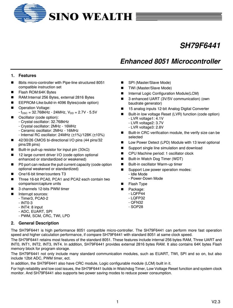
Sino Wealth SH79F6441 User manual

Sino Wealth
Sino Wealth SH79F9661A User manual

Sino Wealth
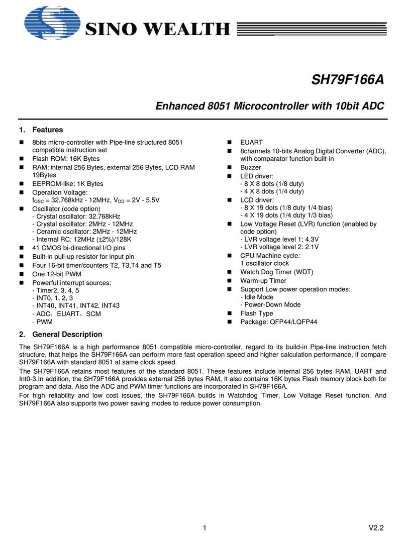
Sino Wealth SH79F166A User manual
Sino Wealth
Sino Wealth SH66L10A User manual

Sino Wealth
Sino Wealth SH79F3283 User manual
Sino Wealth
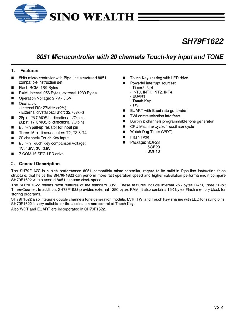
Sino Wealth SH79F1622 User manual
Sino Wealth
Sino Wealth SH79F7416 User manual

Sino Wealth
Sino Wealth SH79F3281A User manual