SOLTEK SL-67EB Plus User manual

1
NOTICE TO END USERS
This User‘ s Guide & Technical Reference is for assisting system
manufacturers and end-users in setting up and installing the mainboard.
Every effort has been made to ensure that the information in this manual is
accurate. Soltek Computer Inc. is not responsible for printing or clerical errors.
Information in this document is subject to change without notice and does not
represent a commitment on the part of Soltek Computer Inc.
No part of this manual may be reproduced, transmitted, translated into any
language in any form or by any means, electronic or mechanical, including
photocopying and recording, for any purpose without the express written
permission of Soltek Computer Inc.
Companies and products mentioned in this manual are for identification
purpose only. Product names appearing in this manual may or may not be
registered trademarks or copyrights of their respective companies.
SOLTEK COMPUTER INC. PROVIDES THIS MANUAL “AS IS “WITHOUT
WARRANTY OF ANY KIND, EITHER EXPRESS OR IMPLIED, INCLUDING
BUT NOT LIMITED TO THE IMPLIED WARRANTIES OR CONDITIONS OF
MERCHANTABILITY OR FITNESS FOR A PARTICULAR PURPOSE. IN NO
EVENT SHALL SOLTEK COMPUTER INC. BE LIABLE FOR ANY LOSS OR
PROFITS, LOSS OF BUSINESS, LOSS OF USE OR DATA, INTERRUPTION
OF BUSINESS, OR FOR INDIRECT, SPECIAL, INCIDENTAL, OR
CONSEQUENTIAL DAMAGES OF ANY KIND, EVEN IF SOLTEK
COMPUTER INC. HAS BEEN ADVISED OF THE POSSIBILITY OF SUCH
DAMAGES ARISING FROM ANY DEFECT OR ERROR IN THIS MANUAL
OR PRODUCT.
©Copyright 1999 Soltek Computer Inc. All Rights Reserved.
Web site : http://www.soltek.com.tw
E-mail : [email protected]
Edition : September 1999
Version : 1.0
Model : SL-67EB+serials

2
C O N T E N T
CHAPTER 1 INTRODUCTION...............................................................4
nFEATURES............................................................................................4
CPU .......................................................................................................4
CHIPSET..................................................................................................4
L2 CACHE...............................................................................................4
MAIN MEMORY .......................................................................................4
BIOS......................................................................................................5
SUPER I/O FUNCTION ..............................................................................5
OTHER FUNCTIONS..................................................................................5
MAINBOARD LAYOUT WITH DEFAULT SETTING ..........................................6
CHAPTER 2 HARDWARE SETUP.........................................................7
nCPU TYPE CONFIGURATION...........................................................7
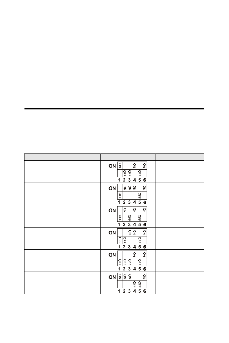
SYSTEM MEMORY CONFIGURATION..........................................................8
BUS RATIO SELECT..................................................................................9
BUS CLOCK SELECT.................................................................................9
nJUMPER SETTINGS..........................................................................10
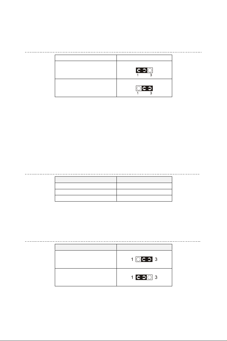
JP2: KEYBOARD POWER SELECT............................................................10
#FAN: ONBOARD FAN (12V) CONNECTOR............................................10
JBAT1: CLEAR CMOS DATA.................................................................10
JP3/JP4: USB PORT SELECT ..................................................................11
JP6: POWER LOST RESUME....................................................................11
JVGA1: VGA CARD.............................................................................11
JWOL1: WAKE ON LAN (WOL) CONNECTOR.......................................11
J2 SWITCH SIGNAL SUMMARY................................................................12
J3 SWITCH SIGNAL SUMMARY................................................................13
nOTHER CONNECTORS....................................................................14
nFLASH MEMORY UPDATE INSTALLATION................................15
CHAPTER 3 BIOS SETUP.....................................................................16
STANDARD CMOS SETUP......................................................................18
BIOS FEATURES SETUP .........................................................................20
CHIPSET FEATURES SETUP .....................................................................25

3
POWER MANAGEMENT SETUP................................................................30
PNP/PCI CONFIGURATION SETUP...........................................................34
LOAD SETUP DEFAULTS .........................................................................37
INTEGRATED PERIPHERALS.....................................................................38
SUPERVISOR/USER PASSWORD...............................................................42
IDE HDD AUTO DETECTION .................................................................43
SAVE & EXIT SETUP ..............................................................................43
EXIT WITHOUT SAVING..........................................................................43

4
Chapter 1
INTRODUCTION
nFEATURES
CPU1. Supports Intel Pentium II/III, Celeron CPUs using SLOT 1 at 233 ~ 700MHz
or higher CPU.
2. Supports CPU voltage auto detect circuit.
3. Supports 66/100MHz Bus Clock with auto detects. (BIOS supports
103/112MHz BUS Clock without auto detects.)
Chipset
1. Intel 82440BX chipset.
2. PCI Rev2.1, 5V, 33MHz interface compliant.
3. Supports AGP 1x/2x Mode, 3.3V AGP (Accelerated Graphics Port) slot.
L2 Cache
1. Pentium II/III supports 256K/512K write back cache with Pipelined Burst
SRAMs.
Main Memory
1. Memory range from 8MB to 768MB with DRAM Table Free configurations.
2. Supports SDRAM with 12/10/8ns DRAM speed.
3. Supports 3pcs 168pin DIMM sockets (3.3V Unbuffered type).
4. DRAM supports ECC or Parity function.

5
BIOS
1. AWARD Plug and Play BIOS.
2. Supports Advanced Power Management Function and ACPI Function.
3. Flash Memory for easy upgrade.
4. BIOS supports CPU Core Voltage Setting.
5. Supports BIOS Writing Protection.
Super I/O Function
1. Integrated USB (Universal Serial Bus) controller with two USB ports.
2. Supports 2IDE channel with 4IDE devices (including ZIP/LS-120 floppy).
3. Provides PCI IDE Bus Master function and supports Ultra ATA33 function.
4. One floppy port.
5. Two high speed 16550 FIFO UART ports.
6. One parallel port with EPP/ECP/SPP capabilities.
7. PS/2 mouse connector.
8. Built-in RTC, CMOS, keyboard controller on single I/O chip.
9. Peripherals boot function (with ATX power).
Other Functions
1. ATX size 17cm x 30.5cm.
2. 5 PCI Master slots, 2 ISA slots and 1 AGP slot.
3. Supports CPU temperature warning function (optional).
4. Provides DIP switch settings.
5. Supports 66/100MHz Bus Clock.
6. Supports keyboard Power on function.
7. Supports Wake On LAN (WOL) function.
8. Supports Power Lost Resume function.
9. BIOS supports 103/112MHz Bus Clock.

6
Mainboard layout with default setting
The default settings of the following figure is for the Celeron / Pentium II
233/66MHz or 350/100MHz.
PCI1
PCI2
PCI3
PCI4
PCI5
AGP
ISA
ISA
Flash BIOS
Slot 1
DIMM1
DIMM2
DIMM3
Intel
440BX
Chipset
Li
Battery
ON
ON
ON
ON
OFF
OFF
OFF
1 2 3 4 5 6
SW1
COM1COM2
LPT1
USB0
USB1 PS/2
K/B
Intel
82371EB
(PIIXE)
ATX Power
FDD 1
IDE 1
IDE 2
1
JBAT1
JVGA
1
JP2
1
JP6
11
JP3
JP4
JWOL1
CFAN1 SFAN1
PFAN1
Upper
Lower
J2
J3
1
1
HDD/LED
SPK RESET KEYLOCK SUSPEND-LED
IR PWR SUSPEND
I/O
Chipset
Clock
Generator
Motherboard layout
NOTE: For 100MHz CPU environment, the SDRAM specification must comply with PC-100
spec.

7
Chapter 2
HARDWARE SETUP
nCPU Type Configuration
The CPU Type Configuration
CPU Model SW1 Setting CPU Ratio
Celeron 233/66
Pentium II / III 350/100 3.5 x
Celeron 266/66
Pentium II / III 400/100 4.0 x
Celeron 300/66
Pentium II / III 450/100 4.5 x
Celeron 333/66
Pentium II / III 500/100 5.0 x
Celeron 366/66
Pentium II / III 550/100 5.5 x
Celeron 400/66
Pentium II / III 600/100 6.0 x

8
Celeron 433/66
Pentium II / III 650/100 6.5 x
Celeron 466/66
Pentium II / III 700/100 7.0 x
Celeron 500/66
Pentium II / III 750/100 7.5 x
Celeron 533/66
Pentium II / III 800/100 8.0 x
System Memory Configuration
This 82440BX mainboard supports 168pin DIMM of 4MB, 8MB, 16MB,
32MB, 64MB, 128MB and 256MB to form a memory size between 8MB to
768MB(SDRAM). 82440BX chipsets provide “Table Free”function. It means
that users can install DRAM with any configuration and in any bank, and that
is why the DRAM table is not needed but do remember that the DRAM must
be 3.3V type.
For 100MHz CPUs environment, the SDRAM specification must comply
with PC-100 spec.

9
Bus Ratio Select
1 2 3 4 5 6
ON
ON
ON
ON
OFF
1 2 3 4 5 6
1 2 3 4 5 6
1 2 3 4 5 6
ON
ON
ON
ON
ON
ON ON
ON ON
OFF
OFF OFF
OFF
OFF
OFF
1 2 3 4 5 6
1 2 3 4 5 6
1 2 3 4 5 6
1 2 3 4 5 6
1 2 3 4 5 6
1 2 3 4 5 6
1 2 3 4 5 6
ON
ON
ON
ON
ON
ON
ON
ON
ON
ON
ON
ON
ON
ON ON
ON ON
ON ON ON
ON
OFF OFF
OFF OFF
OFF
OFF
OFF
OFF
OFF OFF
OFF OFF
OFF
OFF
3.0x
4.5x
6.0x
7.5x
3.5x
5.0x
6.5x
8.0x
4.0x
5.5x
7.0x
SW1 DIP1 ~ DIP4
Bus Clock Select
1 2 3 4 5 6
ON
ON OFF
1 2 3 4 5 6
ON
OFF
OFF
1 2 3 4 5 6
ON
ON OFF
66MHz
100MHz
Auto Detect
(default)
SW1 DIP5 ~ DIP6Bus Clock

10
nJumper Settings
JP2: Keyboard Power Select
Keyboard Power On JP2
Disabled(default)
Enabled
#FAN: Onboard FAN (12V) Connector
#FAN1 Function
CFAN1 CPU FAN
SFAN1 SYSTEM FAN
PFAN1 CHASSIS FAN
JBAT1: Clear CMOS Data
CMOS status JBAT1
Clear CMOS
Retain Data
(Default)
NOTE: 1. If the JP2 is fixed by jumperwire then the board does
not support keyboard power on function.
2. When the keyboard power on function shows any
compatible problem, choose Disabled and report the
keyboard model to the vender/maker.
3. Keyboard power on function must be set from the BIOS.
Refer to the “Integrated Peripherals”section in the
Chapter 3.

11
JP3/JP4: USB Port Select
USB Port JP3 / JP4
Redirect USB port 1 to USB
connector(Default)
Redirect USB 1 to AGP port
JP6: Power Lost Resume
This jumper allows you to use the switch of ATX power supply to control
ON/OFF directly instead of using the power switch on the motherboard.
Power Lost Resume JP6
Normal(default)
Enabled
JVGA1: VGA Card JVGA1
For PCI VGA Card*
Normal (Default)
JWOL1: Wake On LAN (WOL) Connector
This connector is designed to use Lan to bootup the system. Connect the wake
on signal from Lan card to this connector.
NOTE: This jumper is set for the PCI VGA card. Open this jumper
when the system isn’t able to boot up. If you use AGP
card, it is important to set default with JVGA1.

12
J2 Switch Signal Summary
J2 Pin Signal Description
1+5V
2HDD LED Signal
3HDD LED Signal
HDD LED Connector
4+5V
N.C. 5No Connection
6Infrared Transmit Signal
7GND
8Infrared Receive Signal
(low speed)
9Infrared Receive Signal
(high speed)
Infrared Connector
10 +5V
N.C. 11 No Connection
12 GND
PWR 13 Power Switch(for ATX Power)
14 SUSPEND signal
SUSPEND 15 GND
IDE LED Activity Light (J2 pin1-4)
This connector connects to the hard disk activity indicator light on the case.
Infrared Port Module Connector (J2 pin6-10)
The system board provides a 5-pin infrared connector-R1 for an optional
wireless transmitting and receiving module. Pin 6 through 10 are Transmit,
GND, Receive (low speed), Receive (high speed), and Vcc, respectively.
PWR Switch (J2 pin12, 13)
Power Switch: Toggle this pin for turning on/off of the Power supply (for ATX
power only).
SUSPEND Switch (J2 pin14, 15)
Toggle this jumper forces the system to sleep and the system won’t wake up
until the hardware event is coming. (The BIOS Power Management setting
must be enabled.)

13
J3 Switch Signal Summary
J3 Pin Signal Description
1Speaker Signal
2No Connection
3GND
Speaker Connector
4+5V
5Reset Signal
Reset Switch 6GND
N.C. 7No Connection
8+5V
9No Connection
Power LED Connector 10 GND
11 Keylock Signal
Keylock Connector 12 GND
N.C. 13 No Connection
14 SUSPEND LED signal
SUSPEND LED 15 No Connection
Speaker Connector (J3 pin1-4)
The speaker connector is a 4-pin connector for connecting the system and the
speaker. (See the following drawing for jumper position.)
Reset Switch (J3 pin5, 6)
The system board has a 2-pin connector for rebooting your computer without
having to turn off your power switch. This prolongs the life of the system’s
power supply.
Power LED and Keylock Switch (J3 pin8-12)
The keylock switch is a 5-pin connector for locking the keyboard for security
purposes. (See the following drawing for jumper position, and pin1~3 are
connected to power LED and pin 4~5 are connected to keylock switch.)
SUSPNED LED (J3 pin14, 15)
Connect to suspend LED.

14
nOther connectors
123
456
7
•: PS/2 MOUSE ‚: USB0
ƒ: LPT1 „: PS/2 KEYBOARD
…: USB1 †: COM1
‡: COM2
J2
J3
1
1
1
2
3
4
56
7
9
8
•: HDD LED ‚: INFRARED (IR)
ƒ: POWER SWITCH „: SUSPEND CONNECTOR
…: SPEAKER †: RESET SWITCH
‡: POWER LED ˆ: KEYLOCK
‰: SUSPEND LED

15
nFlash Memory Update Installation
1. Download BIOS files and flash utility from your board vendor. They are:
awdflash.exe and .bin file.
2. Copy them to bootable diskette and boot from diskette.
3. The diskette cannot include memory manager e.g. emm386.exe,qemm and
himem.sys, otherwise there will appear an error message “insufficient
memory”.
4. Type "awdflash filename(XXXX.bin)".
5. Next screen will ask you save current bios to file or not? Depend on your
diskette capacity,choose Y or N for this option.
6. Then screen asks you programming the flash memory now? type Y for this
option.
7. Programming finish,utility will ask you reboot system.
8. Reset system and press DEL key enter bios setup screen.
9. Select LOAD SETUP DEFAULTS,press ENTER,press Y,press F10,press Y
10. Finish update procedure.

16
Chapter 3
BIOS SETUP
This mainboard comes with the AWARD BIOS from AWARD Software Inc.
Enter the Award BIOS
Program Main Menu by:
1. Turn on or reboot the system. After a series of diagnostic checks, the
following message will appear:
PRESS <DEL> TO ENTER SETUP
2. Press the <DEL> key and the main program screen will appear as follows.
ROM PCI/ISA BIOS
CMOS SETUP UTILITY
AWARD SOFTWARE, INC.
STANDARD CMOS SETUP
BIOS FEATURES SETUP
CHIPSET FEATURES SETUP
POWER MANAGEMENT SETUP
PNP/PCI CONFIGURATION
LOAD SETUP DEFAULTS
INTEGRATED PERIPHERALS
SUPERVISOR PASSWORD
USER PASSWORD
HDD LOW LEVEL FORMAT
IDE HDD AUTO DETECTION
SAVE & EXIT SETUP
EXIT WITHOUT SAVING
Esc : Quit ¡ô¡õ¡÷:Select Item
F10 : Save & Exit Setup (Shift) F2 : Change Color
Time, Date, Hard Disk Type...

17
3. Using the arrows on your keyboard selects an option, and press <Enter>.
Modify the system parameters to reflect the options installed in your system.
4. You may return to the Main Menu anytime by pressing<ESC>.
5. In the Main Menu, “SAVE AND EXIT SETUP”saves your changes and
reboots the system, and “EXIT WITHOUT SAVING”ignores your changes
and exits the program.

18
Standard CMOS Setup
Standard CMOS Setup allows you to record some basic system hardware
configuration and set the system clock and error handling. You only need to
modify the configuration values of this option when you change your system
hardware configuration or the configuration stored in the CMOS memory gets
lost or damaged.
Run the Standard CMOS Setup as follows:
1. Choose “STANDARD CMOS SETUP”from the Main
Menu and a screen with a list of options will appear.
ROM PCI/ISA BIOS
STANDARD CMOS SETUP
AWARD SOFTWARE, INC.
Date (mm:dd:yy) : Thu, May 9 1996
Time (hh:mm:ss) : 15 : 45 : 10
HARD DISKS TYPE SIZE CYLS HEAD PRECOMP LANDZ SECTOR MODE
Primary Master : Auto 0 0 0 0 0 0 Auto
Primary Slave : Auto 0 0 0 0 0 0 Auto
Secondary Master : Auto 0 0 0 0 0 0 Auto
Secondary Slave : Auto 0 0 0 0 0 0 Auto
Drive A: 1.44M, 3.5 in.
Drive B: None
Video : EGA/VGA
Halt On : All Errors
Base Memory: 640K
Extended Memory: 15360K
Other Memory: 384K
Total Memory: 16384K
Esc : Quit ↑↓→←¡@¡GSelect Item PU/PD/+/- : Modify
F1 : Help (Shift) F2 : Change Color
2. Use one of the arrow keys to move between options and modify the selected
options by using PgUp/PgDn/+/¡Ð keys.

19
A short description of the screen options is as follows:
Date (mm:dd:yy) Set the current date and time.
Time (hh:mm:ss)
Primary This field records the specifications
(Secondary) for all non-SCSI hard disk drives
Master/Slave installed in your system. Refer to
The respective documentation on how
to install the drives.
Drive A/B Set this field to the type(s) of floppy
disk drive(s) installed in your system.
The choices are:
360KB, 5.25 in.,
1.2MB, 5.25 in.,
720KB, 3.5 in.,
1.44M, 3.5 in. (default),
2.88MB, 3.5 in., or None
Video Set this field to the type of video display
card installed in the system. The
choices are:
Monochrome;
Color 40x25;
VGA/EGA (default);
Color 80x25
Halt On Set this warning feature for the type of
errors that will cause the system to halt.
The choices are:
All Errors (default)
No Errors
All, But Keyboard
All, But Diskette
All, But Disk/Key
3. Press <ESC> to return to the Main Menu when you finish setting up the
“Standard CMOS Setup”

20
BIOS Features Setup
BIOS Features Setup allows you to improve your system performance or set up
system features according to your preference.
Run the BIOS Features Setup as follows:
1. Choose “BIOS FEATURES SETUP”from the Main Menu and a screen with
a list of options will appear.
ROM PCI/ISA BIOS
BIOS FEATURES SETUP
AWARD SOFTWARE, INC.
Video BIOS Shadow : Enabled
C8000-CBFFF Shadow : Disabled
CC000-CFFFF Shadow : Disabled
D0000-D3FFF Shadow : Disabled
D4000-D7FFF Shadow : Disabled
D8000-DBFFF Shadow : Disabled
DC000-DFFFF Shadow : Disabled
Virus Warning : Disabled
CPU Internal Cache : Enabled
External Cache : Enabled
CPU L2 Cache ECC Checking : Enabled
Boot Sequence :A,C,SCSI
Swap Floppy Drive : Disabled
Boot Up Floppy Seek : Disabled
Boot Up NumLock Status : On
Gate A20 Option : Fast
Memory Parity/ECC Check : Disabled
Typematic Rate Setting : Disabled
Typematic Rate (Chars/Sec) : 6
Typematic Delay (Msec) : 250
Security Option : Setup
PCI/VGA Palette Snoop : Disabled
ASSIGN IRQ FOR VGA : Enabled
OS Select for DRAMs>64MB : Non-OS/2
Report No FDD For WIN 95 : No
ESC :Quit
¡ô¡õ¡÷
¡ö
: Select Item
F1 :Help PU/PD/+/-: Modify
F5 :Old Values(Shift)F2 : Color
F6 :Load BIOS Defaults
F7 :Load Setup Defaults
2. Use one of the arrow keys to move between options and modify the selected
options by using PgUp/PgDn/+/- keys. An explanation of the <F> keys
follows:
<F1>: “Help”gives options available for each item.
Shift<F2>: Change color.
<F5>: Get the previous values. These values are the values with which the user
started in the current session.
<F6>: Load all options with the BIOS default values.
<F7>: Load all options with the Setup default values.
Table of contents
Other SOLTEK Motherboard manuals

SOLTEK
SOLTEK NF4-754RL User manual

SOLTEK
SOLTEK 85DIR User manual

SOLTEK
SOLTEK SL-67D User manual

SOLTEK
SOLTEK 86SP3 User manual

SOLTEK
SOLTEK SL-65MIV-C User manual

SOLTEK
SOLTEK SL-865G3 User manual

SOLTEK
SOLTEK SL-XP865G-3IG User manual

SOLTEK
SOLTEK B7A-F User manual

SOLTEK
SOLTEK 85ERV2 User manual

SOLTEK
SOLTEK SL-B8D-F User manual

SOLTEK
SOLTEK SL-85DIR3 User manual

SOLTEK
SOLTEK SL-67FV1 User manual

SOLTEK
SOLTEK SL-65ME User manual

SOLTEK
SOLTEK SL-B8E-FG User manual

SOLTEK
SOLTEK SL-865G User manual

SOLTEK
SOLTEK SL-75DRV5 User manual

SOLTEK
SOLTEK SL-85DR-C User manual

SOLTEK
SOLTEK SL-55B5 User manual

SOLTEK
SOLTEK SL-65LIV-T User manual

SOLTEK
SOLTEK SL-53A2 Use and care manual