SOLTEK SL-XP865G-3IG User manual

4
Contents
Con en s
Chap er 1 Specifica ion ............................................. 8
1-1 Mainboard SL-XP865G-3IG Layou ....................................9
1-2 Chipse Sys em Block Diagram........................................... 10
1-3 Mainboard Specifica ion Table ............................................11
1-4 Mainboard Specifica ions .................................................... 12
1-4.1 CPU Socke ................................................................................... 12
1-4.2 Sys em Chipse s ........................................................................... 12
1-4.3 Memory ......................................................................................... 12
1-4.4 AMI BIOS ..................................................................................... 12
1-4.5 In egra ed Mul iplexed AGP and DVO In erface .................. 13
1-4.6 Mul i-I/O Func ions .................................................................... 13
1-4.7 Advanced Sys em Power Managemen .................................... 14
1-4.8 Gigabi LAN on board ................................................................ 14
1-4.9 Hardware Moni or on board ..................................................... 14
1-4.10 RS232/RS422/RS485 In erface suppor ed ............................ 14
1-4.11 Form Fac or ................................................................................ 14
Chap er 2 Hardware Se up ..................................... 16
2-1 CPU Ins alla ion wi h Socke 478B .................................... 17
2-1.1 To Iden ify a Pen ium 4 CPU..................................................... 17
2-1.2 CPU Ins alla ion wi h Socke 478B .......................................... 18
2-2 Pen ium 4 CPU Fan Ins alla ion ......................................... 19
2-3 Memory Ins alla ion ............................................................. 20
2-3.1 To Ins all DDR SDRAM Module .............................................. 20
2-3.2 Dual Channel Memory Modules Se up.................................... 20
2-4 VGA / AGP 8X/4X Slo Ins alla ion.................................... 21
2-5 IDE Connec ors Ins alla ion................................................ 22
2-6 Serial ATA Connec ors Ins alla ion .................................... 23

5
Contents
2-7 Floppy Drive Connec or Ins alla ion ................................. 24
2-8 ATX V2.03 Power Supply Ins alla ion ............................... 25
2-9 PCI/ISA Slo Se up ................................................................ 26
2-10 Jumper Se ings ................................................................... 28
2-10.0 How o ackle he Jumpers: ..................................................... 29
2-10.1 JCLK1 & JCLK2: CPU Frequency Selec ............................ 29
2-10.2 JBAT1: Clear CMOS ................................................................ 30
2-10.3 JPIN1-JPIN6: RS-232/422/485 selec ion for COM2 ........... 30
2-10.4 JKB1: Keyboard/Mouse Wake Up ......................................... 30
2-11 O her Connec ors Configura ion ...................................... 31
2-11.1 On Board Fan Connec ors ....................................................... 31
2-11.2 Thermal De ec or....................................................................... 31
2-11.3 USB Por s and USB Pin-headers ............................................ 32
2-11.4 Chassis Panel Connec ors ........................................................ 33
2-11.5 LAN Connec or on Back Panel ............................................... 33
2-11.6 PS/2 Mouse And PS/2 Keyboard ............................................. 34
2-11.7 COM2 for RS232/RS422/RS485 se up ................................... 35
2-11.8 Complex Pin-header .................................................................. 36
Chap er 3 Sof ware Se up ....................................... 38
3-1 To Open up he Suppor CD ................................................ 38
3-2 In el Chipse Sof ware Ins alla ion U ili y........................ 39
3-3 Direc X Ins alla ion (for Win98se/Me) .............................. 40
3-4 Graphics Driver Ins alla ion ............................................... 41
3-5 To Ins all Hardware Moni or U ili y.................................. 42
3-5.1 Ins alla ion ................................................................................... 42
3-5.2 Verifica ion .................................................................................. 43
3-6 To Ins all LAN Drivers ......................................................... 44
3-6.1 In el 82547EI LAN driver on Windows ME / 2000 / XP....... 44
3-6.2 In el 82547EI LAN driver on Windows 9X............................. 45
3-7 To Ins all USB 2.0 Driver for Windows 2000/XP ............. 47

6
Contents
Chap er 4 AMI BIOS Se up.................................... 48
4-1 Abou BIOS Se up ................................................................. 49
4-2 To Run BIOS Se up ............................................................... 49
4-3 Abou CMOS .......................................................................... 49
4-4 The POST ( Power On Self Tes ) ....................................... 49
4-5 To Upda e BIOS ..................................................................... 49
4-6 BIOS SETUP --- CMOS Se up U ili y................................ 51
4-6.1 CMOS Se up U ili y .................................................................... 51
4-6.2 S andard BIOS Fea ures ............................................................ 53
4-6.3 Advanced BIOS Fea ures ........................................................... 54
4-6.3.1 CPU Configura ion................................................................... 55
4-6.3.2 IDE Configura ion.................................................................... 56
4-6.3.3 Floppy Configura ion ............................................................... 58
4-6.3.4 Super IO Configura ion ........................................................... 59
4-6.3.5 Hardware Heal h Configura ion ............................................. 61
4-6.3.6 ACPI Configura ion ................................................................. 62
4-6.3.7 USB Configura ion ................................................................... 64
4-6.3.8 Power Managemen .................................................................. 65
4-6.3.9 Clock Configura ion ................................................................. 66
4-6.4 Advanced Chipse Fea ures ....................................................... 67
4-6.5 PCI/PNP Resource Managemen .............................................. 70
4-6.6 Boo Configura ion Se up .......................................................... 72
4-6.6.1 Boo Se ings Configura ion .................................................... 73
4-6.6.2 Boo Device Priori y ................................................................. 74
4-6.7 Boo Securi y Fea ures ............................................................... 75
4-6.7.1 Supervisor Password ................................................................ 75
4-6.7.2 User Password........................................................................... 75
4-6.7.3 Change Supervisor Password .................................................. 76
4-6.7.4 Change User Password ............................................................ 77
4-6.7.5 Clear User Password ................................................................ 77
4-6.7.6 Boo Sec or Virus Pro ec ion ................................................... 78

7
Contents
4-6.7 Save Changes and Exi ............................................................... 78
4-6.8 Discard Changes ( and Exi )..................................................... 79
4-6.9 Load Op imal Defaul s ............................................................... 79
4-6.10 Discard Changes ........................................................................ 79
APPENDICES.......................................................... 80
Appendix-1 Iden ify Mainboard Model Number ................... 81
Appendix-2 Technical Terms ...................................................... 82

8
SL-XP865G-3IG
Topics included in this chapter are:
1-1 Mainboard Layout
1-2 Mainboard Specifications**
1-3 Mainboard Specification Table
1-4 Chipset Diagram
Introduction
Chap er 1 Specifica ion
This mainboard features an integration of the powerful processor In-
tel Pentium 4 and the North Bridge Intel 865G. The Intel P4 processor
is a rapid execution engine supporting 800/533/400MHz system bus,
while North Bridge Intel 865G is a high performance chipset providing
Dual Channel DDR 400/333/266 SDRAM memory interface, Hub
interface, AGP interface as well as an integrated Graphics Port for VGA
display.
Integrated with 865G, South Bridge Intel ICH5 supports the LPC I/O,
upstream Hub interface, PCI interface, IDE interface, Serial ATA
interface, USB 2.0 interface, and the interrupt control. This chapter is
to introduce to users every advanced function of this high performance
integration.
** If any difference is found between the mainboard description
and the Mainboard you are using, please look up the Errata/
Update Slip enclosed inside for the correction or updated
information, or else contact the mainboard Dealer or visit our
Web Site for the latest manual update.

9
Chapter 1 Specification
1-1 Mainboard SL-XP865 -3I Layout
mPGA478B
PS/2 K/B (underside)
PW2
BIOS
USB4
1
Fan3
1
ID 1
ID 2
1
ICH5
Intel
Dual Channel DDR 400/333/266MHz
DIMM1
DIMM2
PCI 1
PCI 2
PCI 3
PS/2 Mouse
USB1
FD1
1
INT L
Winbond
LPC I/O
W83627HF
Fan2
1
JBAT1
1
JKB1
(on top)
USB3
1
Battery
Li
+
SPK RST
PWL D
HDD IR PWR
1
20
-
+
-
NJ1
L D
LPT1
COM1
VGA
Intel 82865
Intel
865G
RJ45
(on top)
USB2 (2 Ports)
SATA2
SATA1
ISA3
1
COM2
RT1
AGP1 8X/4X
Main Power
+12V Power
PW1
PCI 4
1
ISA2
ISA1
JPIN1
JPIN6
Fan1
IT
IT8888F
82801 B
1
JCLK1
1
JCLK2
82547 I
(2 Ports
LAN

10
SL-XP865G-3IG
Pentium 4 + Intel 865 + Intel ICH5 Diagram
System Bus 800/533/400MHz
865
266MB/s
Hub Interface
South
Bridge
PCI Bus
ATA 100/66/33
2 IDE
Connectors
USB Bus V2.0
USB
Ports
Intel 82547EI
iga LAN RJ45
IR
FDD
Mouse/Keyboard
Serial Port
Printer Port
Game/MIDI
H/Monitor
BIOS
1-2 Chipset System Block Diagram
A P 8X/4X
VGA
Connector
Intel
Extreme
raphics 2
AGP Slot
DVO(digital)
TV Out
AGP 8X/4X
card
System
Memory
DDR memory
Interface
DDR 400/
333/266
SDRAM
Intel
North Bridge
2 SATA ports Serial ATA
Intel Pentium 4 CPU
(Hyper-Threading Included)
ICH5
LPC I/O
W83627HF
RS232/RS422/RS485
Serial COM Port
IT8888F ISA Slots
PCI Slots
150Mbytes/sec

11
Chapter 1 Specification
1-3 Mainboard Specification Table
XP865 -3I Specifications and Features
CPU
Other Features
Networking
I/O Connectors
PCI Slots
SATA Interface
IDE Interface
AGP interface
I/O Chip
Memory
BIOS
South Bridge
North Bridge
Socket 478B for P4 CPU( HT CPU included)
Keyboard/Mouse Wake Up
Gigabit LAN Controller i82547EI and Connector
RJ45
8 USB2.0 ports, 1 FDD port, 1 COM ports, 1 LPT,
1 RS232/RS422/RS485 Transceiver, 1 IrDA, 1 PS/
2 Keyboard, 1 PS/2 Mouse
4 PCI Master slots on board
2 Serial ATA connectors
2 UATA 66/100 IDE ports
AGP8X/4X Mode only; 1 AGP Slot on board
W83627HF, with Hardware Monitor
Supporting Dual-channel DDR 400/333/266
SDRAM, up to 2GB in 2 DIMM slots
AMI BIOS
Intel ICH5
Intel 865G, supporting 800/533/400MHz FSB
ISA Slot 3 ISA slots on board
Integrated VGA Intel Extreme Graphics2 integrated in 865G

12
SL-XP865G-3IG
1-4 Mainboard Specifications
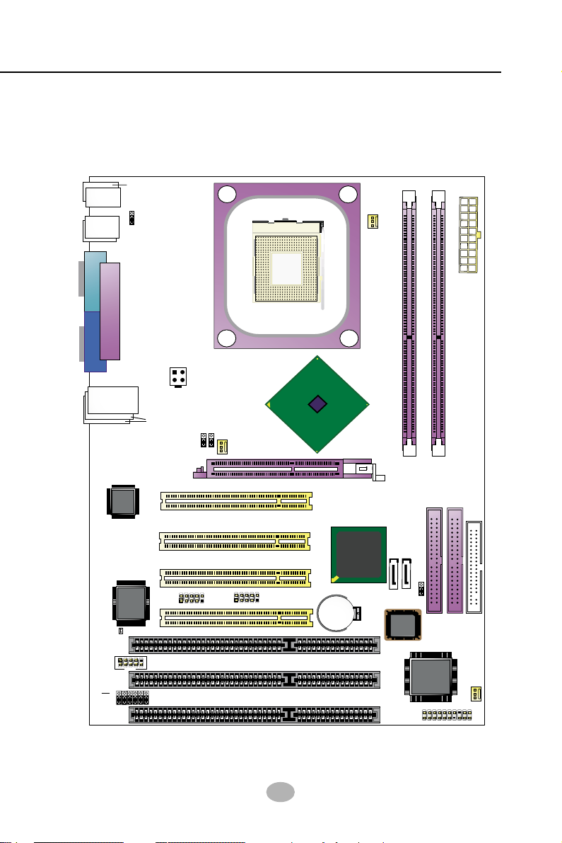
1-4.1 CPU Socket
CPU Socket 478B on board, supporting Intel® Pentium 4 processors
(including Intel Hyper-Threading CPUs) in 478-pin package for :
-- 800/533/400MHz System Bus;
-- Hyper-pipelined technology;
-- Advanced dynamic execution;
-- Advanced transfer cache;
1-4.2 System Chipsets
North Bridge Intel 865G:
• A high performance integrated chipset providing P4 processor interface
(including Hyper-threading Technology), Dual channel DDR 400/333/
266 SDRAM memory, Hub interface, AGP interface as well as an-
other integrated VGA interface with one on-board display port.
• Showing Hyper Threading Logo when booting with a Hyper Thread-
ing CPU.
South Bridge Intel ICH5:
• Supporting the LPC I/O, upstream Hub interface, PCI interface, IDE
interface, Serial ATA interface, USB 2.0 interface, and the interrupt
control.
1-4.3 Memory
2 DDR DIMM 184-pin slots on board :
• Supporting unregistered, non-ECC Dual-channel DDR 400/333/266
SDRAM up to 2GBs
• DIMMs to be populated in identical pairs for Dual-channel operation
• SPD (Serial Presence Detect) Scheme for DIMM Detection supported
1-4.4 AMI BIOS
Flash Memory for easy upgrade, Year 2000 compliant, and supporting
various hardware configuration during booting system (See Chapter 4
BIOS Setup):
• Standard BIOS Features(Times, Date, System Information etc.)
• Advanced BIOS Features (CPU,IDE, Floppy, SuperIO, Hardware
Health, ACPI, USB, and Frequency/Voltage Control)
• Advanced Chipset Features (NorthBridge, SouthBridge Configuration)
• PCI/PNP Resource Management (IRQ Settings, Latency Timers etc.)
• Boot Configuration Setup (Boot Settings, Boot Device Priority etc.)
• BIOS Security Features (Supervisor Password, User Password)

13
Chapter 1 Specification
1-4.6 Multi-I/O Functions
• Serial ATA Controller integrated in ICH5, supporting:
-- 2x Serial ATA connectors supporting up to 150MByte/s transfer rate
• PCI EIDE Controller, supporting:
-- 2x UATA100/66/33 IDE connectors supporting up to 4 IDE devices
• Dedicated IR Functions:
-- Third serial port dedicated to IR function either through the two
complete serial ports or the third dedicated port Infrared-IrDA (HPSIR)
and ASK (Amplitude Shift Keyed) IR
• Multi-mode Parallel Data Transfer:
-- Standard mode, high speed mode ECP and enhanced mode EPP
• Floppy Disk Connector:
-- One FDD connector supporting 2 floppy drives with drive swap support
• Universal Serial Bus Transfer Mode:
-- USB V2.0 compliant; 480Mb/s USB Bus, supporting Windows 2000 or
later operating systems (no support for Windows 9X/ME)
-- 4 built-in USB connectors and 2 USB Headers which require 2 additional
USB cables to provide 4 more optional USB ports
• PS/2 Keyboard and PS/2 Mouse
• UARTs (Universal Asynchronous Receiver / Transmitter):
-- 1 serial port (COM1) on board for RS-232 data transfer;
-- 1serial pin-header (COM2) on board supporting RS-232/422/485 data
transfer;
1-4.5 Integrated Multiplexed A P and DVO Interface
Integrated multiplexed AGP and DVO interface in 865G, supporting AGP
performance and analog/Digital display:
• One AGP slot on board, supporting Digital Video Out card or AGP8x/
4x card for analog/digital display (TMDS,LVDS and TV-out)
(See AGP Installation in Chapter 2 of this manual)
• One 15-pin VGA connector on board, supporting analog display
• Hardware motion compensation assist for software MPEG/DVD de-
code
• Integrated 2D/3D graphics accelerator
• VGA Driver enclosed in Support CD for user’s installation
• ISA Bus: 3x ISA slots integrated on board supported by Chipset
IT8888F for standard ISA cards setup

14
SL-XP865G-3IG
1-4.8 igabit LAN on board
Gigabit Fast Ethernet Controller Intel 82547EI on board:
• Supporting 10/100/1000Mb data transfer
• Supporting Wake On LAN function through the on-board RJ45 LAN
Connector
• LAN Driver enclosed in Support CD for user’s installation.
1-4.9 Hardware Monitor on board
• Hardware Monitor supported by W83627HF, providing monitoring and
alarm for flexible desktop management of hardware voltage, tempera-
tures and fan speeds.
• Utility Software Soltek Hardware Monitor for displaying system status
is enclosed in Support CD for user’s installation.
1-4.7 Advanced System Power Management
• ACPI 1.0B compliant (Advanced Configuration and Power Interface),
including ACPI suspend mode support (See ACPI Configuration of
Advanced BIOS Features in BIOS Setup)
• APM V1.2 compliant (Legacy Power Management)
• Supporting Wake-on-LAN
• Supporting Real Time Clock (RTC) for date alarm, month alarm, and
century field configuration
1-4.10 RS232/RS422/RS485 Interface supported
• COM2 is a serial com port supporting RS232/RS422/RS485 interface
serial data communications;
• JPIN1 to JPIN6 are jumpers designed to set COM2 to RS232/RS422/
RS485 interface.
1-4.11 Form Factor
• ATX Form Factor, ATX Power Supply, version 2.03 compliant, sup-
ported by one Main Power Connector, one +12V Power Connector.
• Mainboard size: 305mm x 220mm

15
Chapter 1 Specification
Memo

16
SL-XP865G-3IG
Chap er 2 Hardware Se up
1. We recommend to install your CPU before any other components.
For detailed installation instructions of processor, you can also refer
to the pamphlet enclosed in your CPU package.
2. Installing a cooling fan with a good heat sink is a must for proper
heat dissipation for your CPU. Get ready an appropriate fan with
heat sink for proper installation. Improper fan and installation will
damage your CPU.
3. In case CPU Vcore, CPU clock or Frequency Ratio is adjustable on
board, please follow the instructions described in the User’s manual
for proper setup. Incorrect setting will cause damage to your CPU.
The following topics are included in this chapter:
To et Things Ready for Hardware Setup !
2-1 CPU Installation with Socket 478B
2-2 Pentium 4 CPU Fan Installation
2-3 Memory Installation
2-4 V A / A P 8X/4X Slot Installation
2-5 IDE Connectors Installation
2-6 Serial ATA Connectors Installation
2-7 Floppy Drive Connector Installation
2-8 ATX V2.03 Power Supply Installation
2-9 Jumper Settings
2-10 Other Connectors Configuration
2-11 PCI/ISA Slot Setup

17
Chapter 2 Hardware Setup
2-1 CPU Installation with Socket 478B
1) CPU Working Frequency
On the heatsink side of a Pentium 4 CPU, there printed a line of figures
to identify its specifications. The line consists of 4 parts:
1. CPU Working Frequency: this part depicts the working frequency of
the CPU. The Intel P4 processor with three differeent System Bus
mode provides a variety of speeds ranging from 2A Ghz to 3.2Ghz.
400MHz System Bus: 2.60, 2.50, 2.40, 2.20, 2A GHz
533MHz System Bus: 3.06, 2.80, 2.66, 2.53, 2.40, 2.26 GHz
800MHz System Bus: 3.20, 3, 2.80C, 2.60C, 2.40C GHz
2. CPU L2 Cache: this part depicts the L2 Cache size. For example,
512 stands for 512 KB L2 Cache; 256 stands for 256 KB L2 Cache
3. System Bus: this part depicts the System Bus (Front Side Bus) is
provided by CPU clock x 4. For example,
800MHz = 200MHz(CPU clock) x 4; 533MHz = 133MHz x 4
400MHz = 100MHz x 4
Note: System Bus vs CPU Clock
P4 CPU is a quad-pumped CPU. The system bus is provided by the
CPU clock x 4. Therefore, users can figure out the P4 CPU clock by the
System Bus divided by 4.
(Hyper-Threading CPU included)
Intel
PENTIUM 4
2.80 Hz / 512 / 800
2) CPU L2 Cache
3) System Bus
Pentium 4 with Hyper Threading Technology :
The new P4 processors at 2.40C, 2.60C, 2.80C, 3, 3.20GHz with an
advanced 800MHz system bus and P4 processor at 3.06Ghz with
533MHz system bus support Hyper Threading Technology.
2-1.1 To Identify a Pentium 4 CPU

18
SL-XP865G-3IG
mPGA478B
Intel Pentium 4
mP A478B
Pin 1
2-1.2 CPU Installation with Socket 478B
This mainboard is built with CPU
Socket 478B ( 478-pin) supporting
the Intel Pentium 4 CPU:
• Follow the steps described in this
section to install the 478-pin Pen-
tium 4 CPU into the on board
Socket 478.
• After installation of Pentium 4 CPU,
you must also install the specific
Pentium 4 CPU fan designed in
tandem with this CPU. This CPU
Fan installation is described in next
section.
• This mainboard supports Hyper-
threading dual-in-one CPU, the
function of which can be enabled
by Windows XP. (See illustration
on the right.)
1. First pull sideways the lever of
Socket 478, and then turn it up
900 so as to raise the upper layer
of the socket from the lower
platform.
3. Make sure that all CPU pins have
completely entered the socket
and then lower down the lever
to lock up CPU to socket.
2. Configure Pin 1 of CPU to Pin 1
of the Socket, just as the way
shown in the diagram on the
right. Adjust the position of CPU
until you can feel all CPU pins
get into the socket with ease.
mPGA478B
Intel Pentium 4
Pin 1
( If Hyper-threading CPU is
installed successfully with O/S
Win XP, the O/S will enable the
dual-in-one CPU function.)

19
Chapter 2 Hardware Setup
2-2 Pentium 4 CPU Fan Installation
Connect Fan Connector to CPU FAN connector
Pentium 4 Fanbase
CPU Fan Connector
The above pictures are taken from sample mainboards as installation illustr-
ation. The layout in the pictures may be different from your mainboard.
Press down 2 Spring Locks to lock fan to fanbase

20
SL-XP865G-3IG
184-Pin DIMM Notch Key Definitions
DRAM Key Position Voltage Key Position
2-3.1 To Install DDR SDRAM Module
• To enable Dual Channel memory function, users should insert totally
identical (size and frequency) DDR module pair into the bank-pair.
DDR Rib
(2.5V Voltage Key)DDR Notch
184-Pin DIMM Notch Key Definition
DIMM1
DIMM2
DIMM1+DIMM2 = Dual Channel Memory
Module Latch
2-3 Memory Installation
• Make sure to unplug your power supply before adding or removing
memory module.
• Pay attention to the orientation of the DIMM slots.
• Dual Channel memory configuration provides higher performance than
Single Channel configurations
• Matched DIMMs need to have identical density, DRAM technology,
DRAM bus width, and equal number of memory banks.
• This series supports up to 2GB unbuffered Dual-channel DDR 400/
333/266 SDRAM, with 2 DDR DIMM slots on board. Do not insert
other type of modules into these slots.
• The dual memory controller can double the DDR memory bandwidth
up to 6.4GB/s with DDR400, 5.4GB/s with DDR333 and 4.2GB/s with
DDR266.
2-3.2 Dual Channel Memory Modules Setup
• DDR DIMM slot has 184 pins and one notch. Insert a DDR SDRAM
vertically into the 184-pin slot with the notch-to-rib matching.

21
Chapter 2 Hardware Setup
mPGA478B
PS/2 K/B (underside)
PW2
BIOS
USB4
1
Fan3
1
ID 1
ID 2
1
ICH5
Intel
Dual Channel DDR 400/333/266MHz
DIMM1
DIMM2
PCI 1
PCI 2
PCI 3
PS/2 Mouse
USB1
FD1
1
INT L
Winbond
LPC I/O
W83627HF
Fan2
1
JBAT1
1
JKB1
(on top)
USB3
1
Battery
Li
+
SPK RST
PWL D
HDD IR PWR
1
20
-
+
-
NJ1
L D
LPT1
COM1
VGA
Intel 82865
Intel
865G
RJ45
(on top)
USB2 (2 Ports)
SATA2
SATA1
ISA3
1
COM2
RT1
AGP1 8X/4X
Main Power
+12V Power
PW1
PCI 4
1
ISA2
ISA1
JPIN1
JPIN6
Fan1
IT
IT8888F
82801 B
1
JCLK1
1
JCLK2
82547 I
(2 Ports
LAN
1. To install on-board VGA, please connect your monitor directly to VGA
connector on board.
2-4 V A / A P 8X/4X Slot Installation
2. To install AGP 8X/4X card / Digital-Video-Out(DVO) / TV Out display,
please insert an AGP / DVO /TV Out card into the AGP slot. This
AGP slot supports AGP 8X/4X card(analog), DVO card and TV Out
card, respectively but not simultaneously.
V A
Connector
LCD (digital)
Monitor
DVI
Connector
DVI Cable
DVO Card
TV Out Display
(analog)
Analog
Monitor
Insert an A P 8X/4X card / DVO / TV Out card to A P slot for
A P / DVO / TV Out Display

22
SL-XP865G-3IG
mPGA478B
PS/2 K/B (underside)
PW2
BIOS
USB4
1
Fan3
1
ID 1
ID 2
1
ICH5
Intel
Dual Channel DDR 400/333/266MHz
DIMM1
DIMM2
PCI 1
PCI 2
PCI 3
PS/2 Mouse
USB1
FD1
1
INT L
Winbond
LPC I/O
W83627HF
Fan2
1
JBAT1
1
JKB1
(on top)
USB3
1
Battery
Li
+
SPK RST
PWL D
HDD IR PWR
1
20
-
+
-
NJ1
L D
LPT1
COM1
VGA
Intel 82865
Intel
865G
RJ45
(on top)
USB2 (2 Ports)
SATA2
SATA1
ISA3
1
COM2
RT1
AGP1 8X/4X
Main Power
+12V Power
PW1
PCI 4
1
ISA2
ISA1
JPIN1
JPIN6
Fan1
IT
IT8888F
82801 B
1
JCLK1
1
JCLK2
82547 I
(2 Ports
LAN
2-5 IDE Connectors Installation
To install IDE Connector, you may connect the blue connector of IDE
cable to the primary (IDE1) or secondary (IDE2) connector on board,
and then connect the gray connector to your slave device and the black
connector to your master device. If you install two hard disks, you must
configure the second drive to Slave mode by setting its jumpers correctly.
Please refer to your hard disk documentation for the jumper settings.
IDE Flat Cable
Orient the red line on the IDE
Flat Cable to Pin1.
Pin 1 (to Red Line)
Hard Disk Drive Connector
IDE1
IDE2
Gray connector
Blue connector
Black connector
Red line
(To Mainboard)
(To Slave device)
(To Master Device)
80-conductor
cable

23
Chapter 2 Hardware Setup
mPGA478B
PS/2 K/B (underside)
PW2
BIOS
USB4
1
Fan3
1
ID 1
ID 2
1
ICH5
Intel
Dual Channel DDR 400/333/266MHz
DIMM1
DIMM2
PCI 1
PCI 2
PCI 3
PS/2 Mouse
USB1
FD1
1
INT L
Winbond
LPC I/O
W83627HF
Fan2
1
JBAT1
1
JKB1
(on top)
USB3
1
Battery
Li
+
SPK RST
PWL D
HDD IR PWR
1
20
-
+
-
NJ1
L D
LPT1
COM1
VGA
Intel 82865
Intel
865G
RJ45
(on top)
USB2 (2 Ports)
SATA2
SATA1
ISA3
1
COM2
RT1
AGP1 8X/4X
Main Power
+12V Power
PW1
PCI 4
1
ISA2
ISA1
JPIN1
JPIN6
Fan1
IT
IT8888F
82801 B
1
JCLK1
1
JCLK2
82547 I
(2 Ports
LAN
2-6 Serial ATA Connectors Installation
The Serial ATA is designed to improve the Parallel ATA with the capabil-
ity of Hot Plug and offer a data bandwidth of 150Mbytes/second. It also
reduce voltage and pin count and can be implemented with thin cables
which improve the inner ventilaton of PC cases.
2 Serial ATA connectors are built on board, supported by the ICH5 SATA
Controller for SATA Hard Disk Drives.
Serial ATA Connectors
Serial ATA Hard Disk
Serial ATA Cable
Serial ATA Power Cable
To Power Supply
SATA Power Connectors
Table of contents
Other SOLTEK Motherboard manuals

SOLTEK
SOLTEK SL-75DRV5 User manual

SOLTEK
SOLTEK KT400-R User manual

SOLTEK
SOLTEK SL-85DRV+ User manual

SOLTEK
SOLTEK SL-63AV User manual

SOLTEK
SOLTEK 85DR2-DC User manual

SOLTEK
SOLTEK SL-65EP User manual

SOLTEK
SOLTEK K8AV2-R User manual

SOLTEK
SOLTEK SL-85SD-C User manual

SOLTEK
SOLTEK 75DRV User manual

SOLTEK
SOLTEK SL-65DRV User manual

SOLTEK
SOLTEK KT333A User manual

SOLTEK
SOLTEK SL-65LIV-T User manual

SOLTEK
SOLTEK 85DRV4-C User manual

SOLTEK
SOLTEK SL-67EZ Use and care manual

SOLTEK
SOLTEK 85DRV5-L User manual

SOLTEK
SOLTEK SL-845GLI User manual

SOLTEK
SOLTEK SL-55B5 User manual

SOLTEK
SOLTEK SL-65ME User manual

SOLTEK
SOLTEK 85DIR User manual

SOLTEK
SOLTEK SL-B9D-FGR User manual