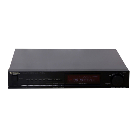
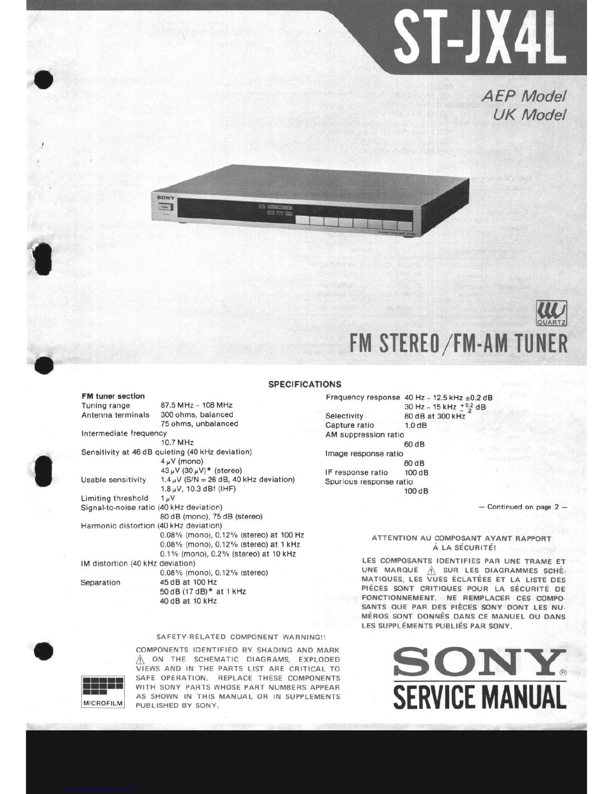
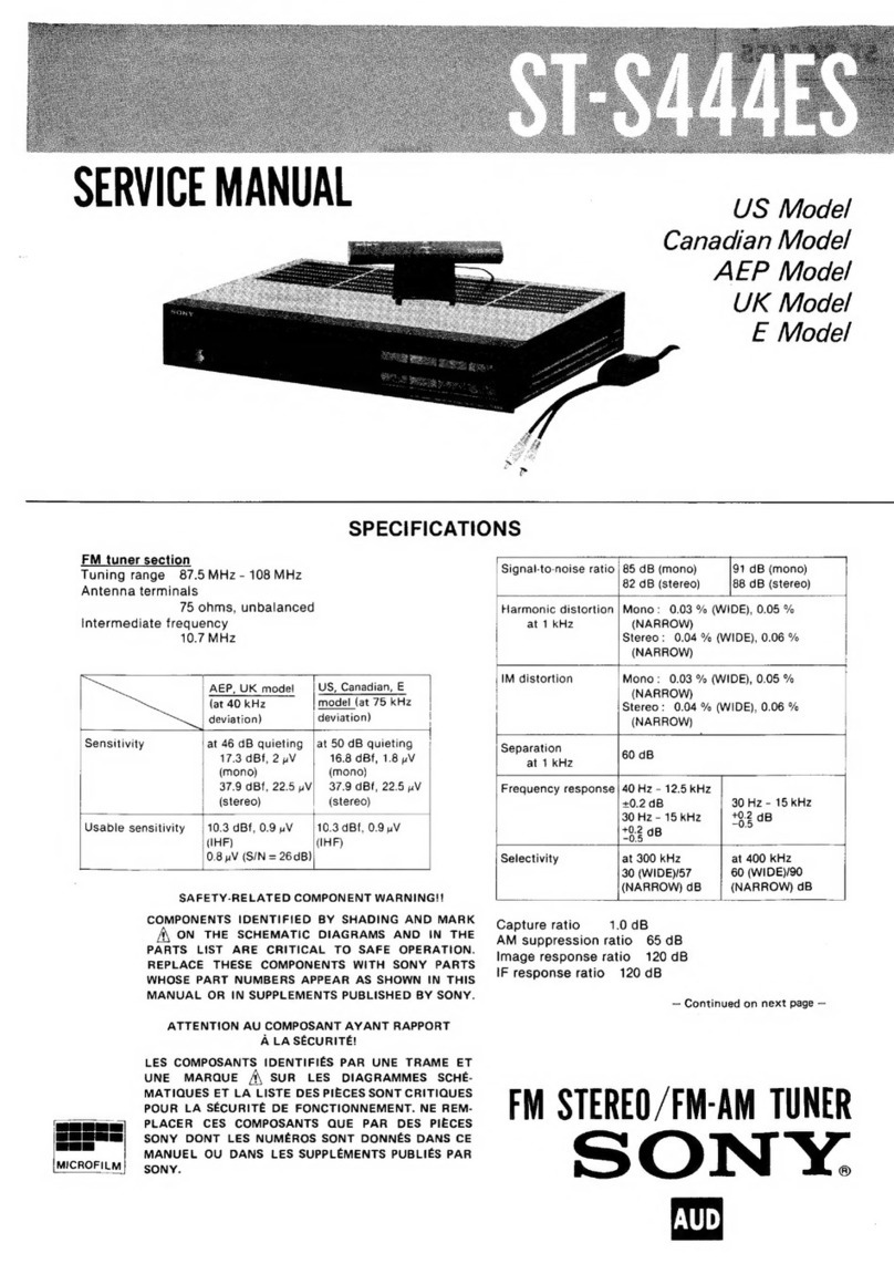
Sony ST-JX4L User manual

AEP Model
UK Model
tM
$TtnE0/Fn||-A]r{
TlJ
rwl
IQUARTZI
N,[fi
Frequency
response
40Hz
- 12.5kH'z
+0.2
dB
30
Hz
- 15
kHz
1oà2
dB
Selectivity 80dBat300kHz
Captureratio 1.0dB
AM
suppressionratio
60dB
lmage
responseratio
80dB
lFresponse
ratio 10OdB
Spuriousresponse
ratio
100
dB
- Continued on page 2 -
ATTENTION AU COMPOSANTAYANT RAPPORT
Àu sÉcunrrÉr
LES COMPOSANTSIDENTIFIES PAR UNE TRAME ÊT
urue ruenoue I suR LEs DTAGRAMMEs
scxÉ-
MATrouEs,
LEsvuEs ÉclerÉes ET LA Ltsrg DEs
prÉces
soNT cRrrrouEs
pouR le sÉcuntrÉ oe
FONCTIONNEMENT. NE REMPLACER CES COMPO-
sANTsouE pARoes prÈces
soNy DoNT LEsNU-
nnÉnos
sorur ooruruÉs
DANscE MANUEL
ou DANS
les suppt-ÉueNrs
puelrÉspAR
soNy.
SONY
FM tuner section
Tuningrange 87.5
MHz
- 108MHz
Antennaterminals 300ohms,balanced
75
ohms,unbalanced
Intermediate
frequency
10.7MHz
Sensitivity
at 46dB quieting
(40
kHz
deviation)
4
sV (mono)
43gV(30pV)i (stereo)
Usable
sensitivity 1.4FV
(S/N
= 26dB,40kHz
deviation)
1.8
sV,
10.3dBf
(lHF)
Limiting
threshold 'l
sV
Signal-to-noise
ratio(40
kHzdeviation)
80dB (mono),
75dB (stereo)
Harmonicdistortion
(40
kHzdeviation)
0.08%
(mono)
,0.12o/o
(stereo)
at '100
Hz
0.08%
(mono),
0.12o/o
(stereo)
at 1
kHz
0.1%(mono),
0.2%(stereo)
at 10kHz
lM clistortion
(40
kHzdeviation)
SPECIFICATIONS
0.08% (monol, O.12% (stereo)
45 dB at 100 Hz
50dB (17d8)* at 1kHz
40 dB at 10kHz
SAFETY.RELATED COMPONÊNTWARNING!
!
COMPONENTS
IDENTIFIEDBY SHADING AND MARK
A oN THE scHEMATrc DTAGRAMS, EXpLoDED
VIEWSAND IN THE PARTS LIST ARE CRITTCAL
TO
SAFE OPERATION. REPLACE THESE COMPONENTS
WITH SONY PARTS WHOSE
PART NUMBERS APPEAR
AS SHOWN IN THIS MANUAL OR IN SUPPLEMENTS
PUBLISHEDBY SONY.
Seoaration
SERVICE
MANUAL

sT-JX4L
RF
intermodulation
74dB
(lHF),
88dB
(2.4
MHz)
Sub-carrier
product
ratio
55
dB
Muting
threshold Approx.
25.2dBl,
10
yY
Output
level/impedance
(75
kHzdeviation)
750
mV,4.7k ohms
Calibrating
tone
level
' 50%
modulation
(37.5
kHz
deviation),
400Hz
( )* measuredwith
theSENSswitchengaged
MW/LW
tunersection
Ferriterod antenna
External
antenna
terminal
54(50)' dB/m
(at 230kHz)
50(40)t sV
(at 230 kHz)
45dB(9
kHz)
75dB (at230
kHz)
( )r measurèd with the SENS switch engagod
46(42)* dB/m
(at999
kHz)
40
(30)*
rV
(at
999
kHz)
45dB (at999kHz)
General
System
Power
requirements
Powerconsumption
Dimensions
Weight
PLL
quartz-locked
digital
synthesizer
system
UKmodef : 24OV ac-lor22OY ac-adjust-
ableby authorized
Sony personnel),
50/60 Hz
AEP modef: 22OY ac- lor 24OY ac
- adlust-
ableby authorized
Sony personnel),
50/60 Hz
12W
Approx.
430
x 55
x 330
mm
(w/h/d)
(17
x 2rlt
x 13inches)
including
projecting
parts
andcontrols
Approx.3.6
kg
(7
lbs
15
oz)
net
Approx.
4.1
kg
(9
lbs
1
oz)
inshipping
carfon
MODEL
lDENTIFICATION
- Specification
Label-
AEPmodel MODELNO.
ST. JX4L
FMSTEREO/FM.AM
TUNER
FREQUINCY
RANGE'
FM875-l08MHzMW522-1602kHz
LWl55-344kHz
lF :
FM
l0.7MHzAM450kHz
AC:22QV
- 50/60H2 tzW
FTZ-PRÙFNUMMER
U185
SERIAL
NO.
MADE
IN JAPAN 4-875-305-OI
OUK model
MODEL
NO.
ST-JX4L
FMSTEREO/FM-AMTUNER
FREQUENCYRANGE:
FM87.5-l08MHz
MW522-l602kHz
LW
155
-
344
kHz
:FM
l0.7MHz
AM450kHz
50/60H2 tzW
AC:240V-
SERIAL
NO,
MADE
IN
JAPAN 4-875-306-0I
2-

ST.JX4L
. THE CERAMIC CAPACITORS
This set uses tube-type ceramic capacitors whose
shape is identical with the carbon resistors. Be careful
not to use resistorsinstead of capacitorsin repairing'
Disc-type ceramic capacitors can be used for
replacing those originally used in the set.
Two kinds of drilled holes are provided in some
patterns for mounting the tube-type and disc-type
ceramic capacitors. Use appropriate holes where
applicable.
Silvering on inside
of tube forming
second electrode.
SERVICING
NOTES
Example:
ceramtc
't
st digit temperature
characteilstic
tolerance
yellow
;
47 l0'15%
wh.ite
SL ) 47OpF +5% SL
Silvering deposited on outside
of tube forming one electrode.
multiplier
2nd digit
COLOR
CODE(in PFI
Color lst or 2nd
Digit Multipliet Tolerance Temperatur€
charac-
teristac
brown Il0' Y
red 21o'? D
orange J103
yellow 410" RH
gleen 5
blue 6
violel 7UJ
Elay 8x30Vo x
white 9SL
black 0100 t207o CH
eold l0-t t5% V
silver t0-? xlÙVo B
3-

ST-JX4L
o Handling
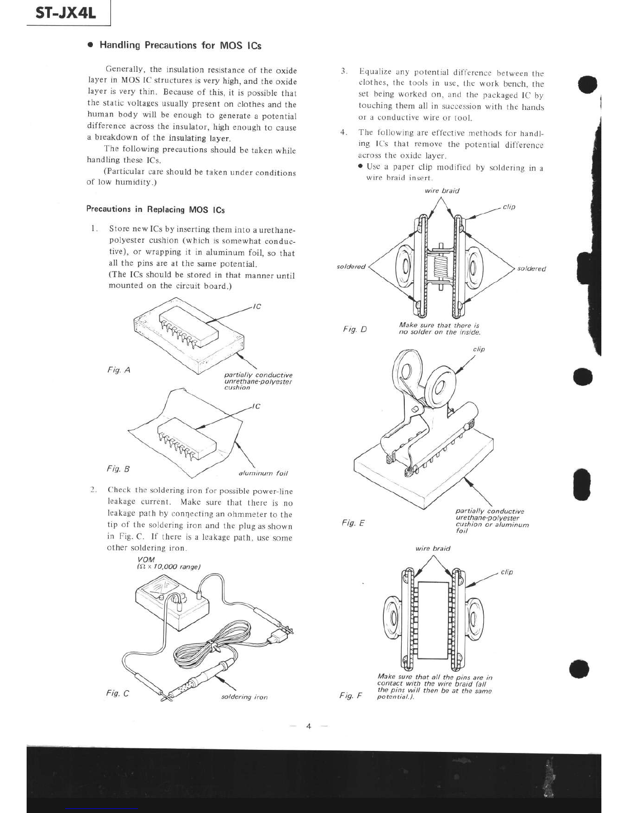
Precautions
for MOSlCs
Generally, the insulation resistance
of the oxide
layer in MOS IC structures
isveryhigh,
and the oxide
layer is very thin. Because
of this, it is possible
that
the static voltages
usually present
on clothesand the
human body will be enough to generate
a potential
difference across
the insulator, high enough to cause
a breakdown of the insulating
layer.
The following precautions
should be takenwhile
handlingthese
ICs.
(Particular care
should
be taken under conditions
of low humidity.)
Precautions
in ReplacingMOS lCs
Store
newICsby inserting
them into aurethane-
polyester cushion (which is somewhat conduc-
tlve), or wrapping it in aluminum foil, so that
all the pins areat the same
potential.
(The ICs shouldbe stored in that manner
until
mounted on the circuit board.)
Fis. Apartially conductive
unrethane-polyeste r
cushion
Fis. Baluminum foil
Equalize
any potential
difference
between
the
clothes,
the tools in use,
the work bench,
the
set being
worked on, and the packaged
IC by
touching them all in succession
with the hancis
or a conductive
wireor tool.
The following are effective methods for handl-
ing ICs that remove the potential difference
across
the oxide layer.
. Use a paper clip nrodified by solderingin a
wire braid
insert.
3.
soldered
Fig. D
Fis. E
soldered
oI
I
o
I
2
Make sure that there is
no solder on the inside
clip
Check the soldering
iron for possible
power-line
leakagecurrent. Make sure that there is no
leakage
path
by con4ecting
anohmmeter
to the
tip of the soldering
iron and the plug
as
shown
in Fig.
C. If there is a leakage
path, use
some
other solderins
iron.
VOM
(dl x IO,OOO range)
Make sure that all the oins are in
contact with the wire braid latt
_ the pins will then be at the same
f tg. f potentiat.).
partially conductive
urethane-polyeste r
cushion or aluminum
foil
wire braid
wire braid
Fis.
4-

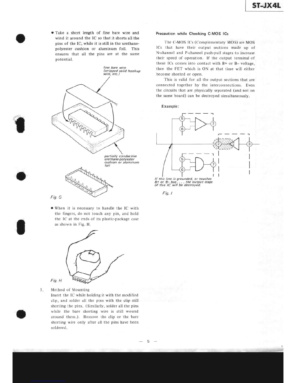
OTake a short length of fine bare wire and
wind it around the IC sothat it shorts all the
pins of the IC, while it is still in the urethane-
polyester cushion or aluminum foil. This
ensures that all the pins are at the same
potential.
fine bare wire
(stripped solid hookup
wtre, etc.J
Precaution
while Checking C-MOS lCs
The C-MOSICs (Complementary MOS) areMOS
ICs that have their output sections made up of
N-channeland P-channel
push-pullstagesto increase
their speedof operation. If the output terminal of
these ICs comesinto contact with B+ or B- voltage,
then the FET which is ON at that time will either
becomeshorted or open.
This is valid for all the output sectionsthat are
connected together by the interconnections. Even
the circuits that are physically separated
(and not on
the same board) can be destroyed simultaneously.
Example:
I
partially conductive
urethane-polyester
cushion or aluminum
foil
Fis.G
o When it is necessary
to handle the IC with
the fingers,do not touch any pin, and hold
the IC at the endsof its plastic-package
case
asshown in Fig.H-
Fis. H
Method of Mounting
Insert the IC while holding it with the modified
clip, and solder all the pins with the clip still
shortingthe pins. (Similarly, solderall the pins
while the bare shorting wire is still wound
around them.). Remove the clip or the bare
shorting wire only after all the pins havebeen
soldered.
lf this line is grounded, or touches
B+ or B- bus. . . , the output stage
of this lC will be destroyed.
Fis. I
5-

SECTION
1
OUTLINE
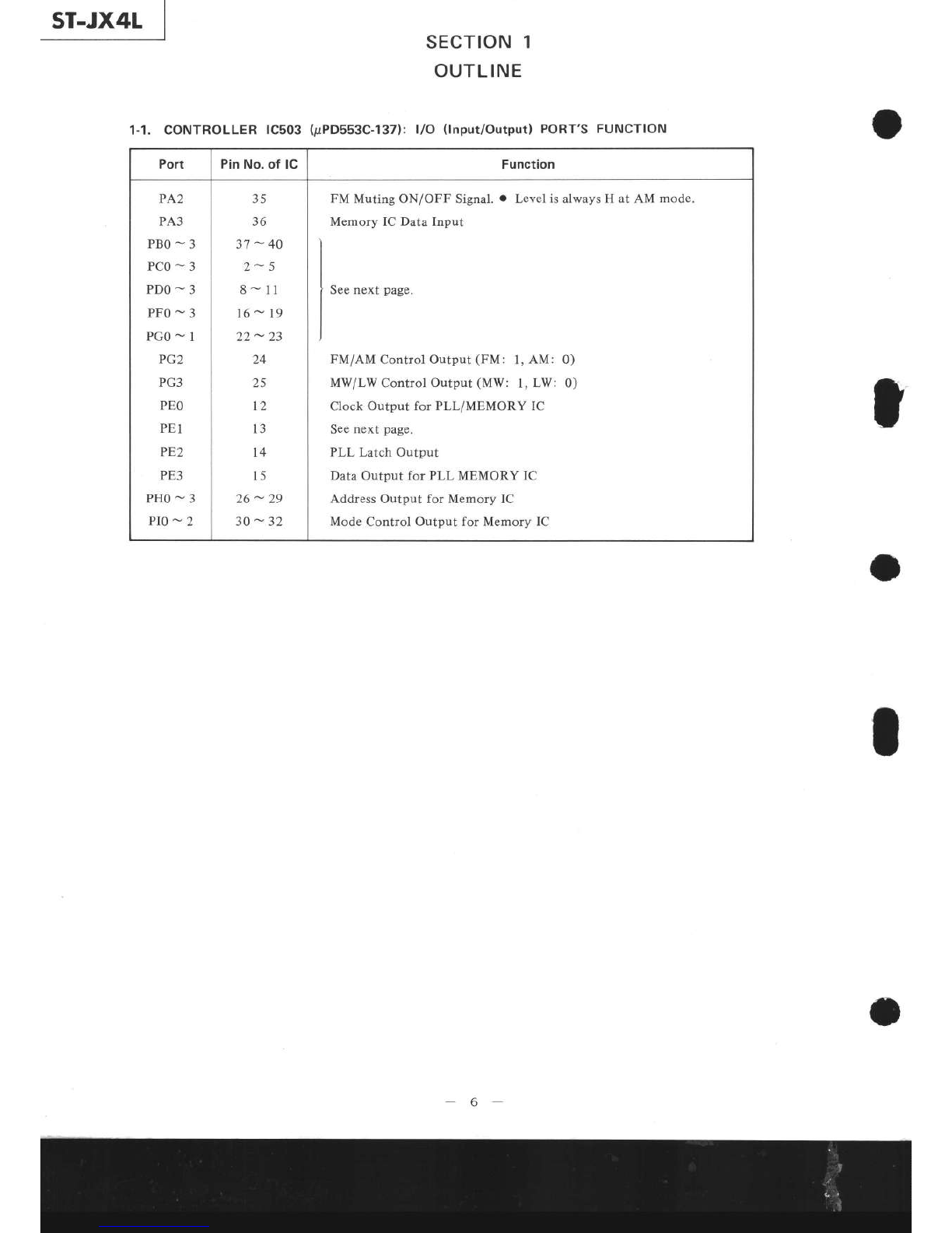
1-1. CONTROLLER
1C503
(1rPD553C-1371:
llO (lnput/Output)PORT'SFUNCTION
Port PinNo.of lC Function
PA2
PA3
PBO-3
PCo-3
PDO-3
PFO-3
PGO-l
PG2
PG3
PEO
PEI
PE2
PE3
PHO-3
Pto-2
J)
36
37-40
2- 5
8-11
t6-19
22-23
24
25
t2
t3
14
15
26-29
30-32
FM Muting ON/OFF Signal.
Memory IC Data Input
Level is alwaysH at AM mode.
Seenext page.
FM/AM Control Output (FM: I, AM: 0)
MWLW Control Output (MW: I, LW: 0)
Clock Output for PLL/MEMORY IC
$ee
next page.
PLL Latch Output
DataOutput for PLL MEMORY IC
Address Output for Memory IC
Mode Control Output for Memory IC
6-

5T-JX4L
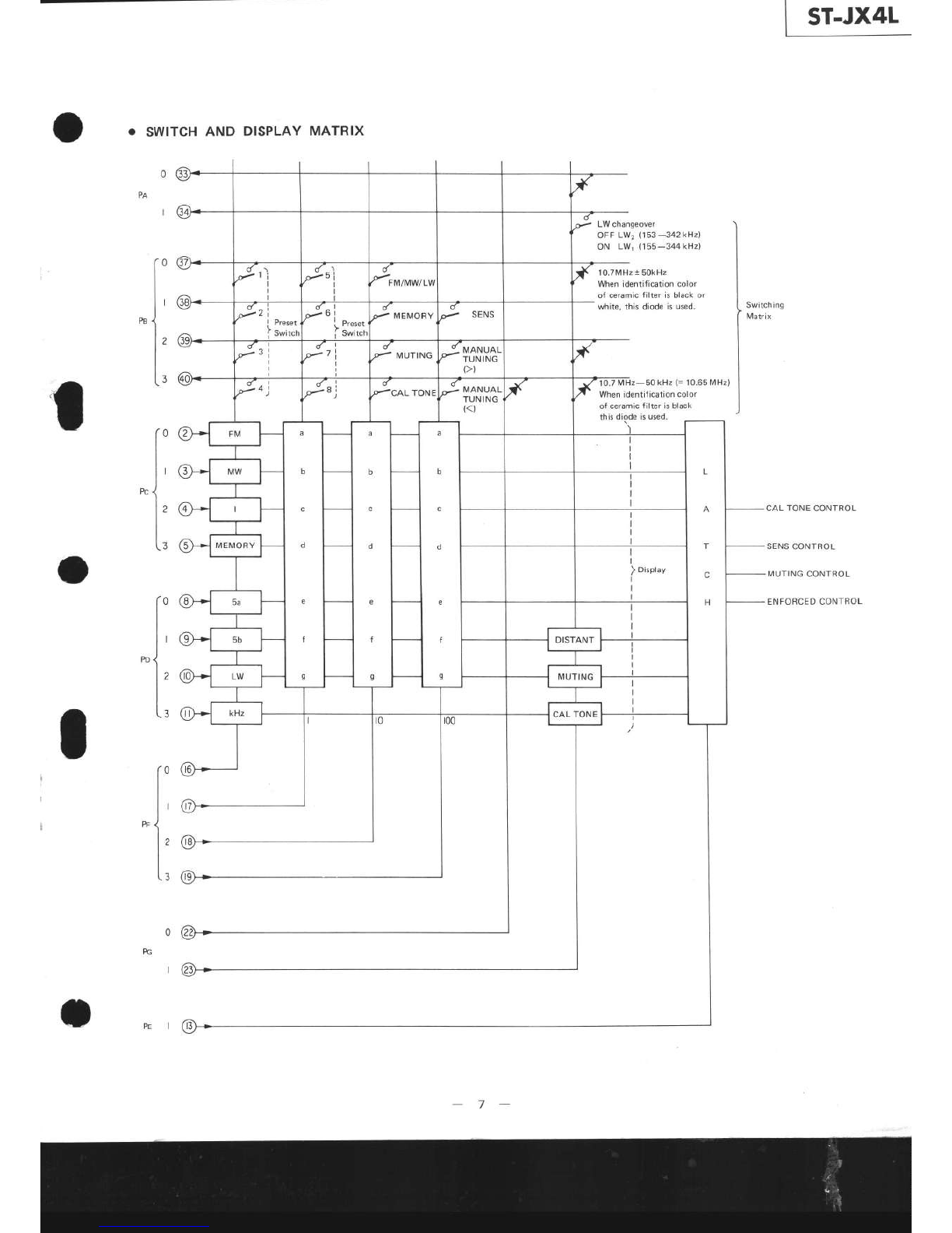
O SWITCH
AND DISPLAY
MATRIX
10.7MHz I 50kHz
When identitication color
of ceramic filter is blôck or
white, this diode is used.
LW changeover
OFF
Lw, (153-342
kHz)
ON LW,
(155-344
kHz)
kHz
(=
19.6ttt.,
Switching
Matrix
When identiTication
colol
ol ceramic filter isblack
this diode isused
CAL TONE CONTROL
SENSCONTROL
'MUTING
CONTROL
ENFORCEDCONTROL
7-

ST.JX4L
1-2. BLOCK
DIAGRAM
LEIEr
E
L-El---l
L!
=
v
.I
F]
g
Ëtr
IJ
à
l,'l
g
FI
E
oF<
aÈ
Èt
t:i
frf,
* ==r
.l
I
t_
t*
I
I
8-

1.3. TUNING WITH THE STATION PRESET
BUTTONS
With this tuner, owing to an electronic tuning
system using a PLL (Phase
Locked Loop) synthesizer
and a memory circuit, the reception of a station is
much simplified. Once you commit the frequencies to
memory, pushing
a button isall you need
do to select
a desired station. There is no need to search for the
station with the TUNING button each
time you wish
to tune in a station.
TO MEMORIZE THE STATION FREOUENCIES
Preparation: A total of eight station preset but-
tons can be preset for either FM, MW or LW in any
desired sequence. Arrange the order of stations for
each station preset button and note the band and the
frequencyof each
in advance.
Repeat
these
stepsfor each
stationpreset
button.
Replace the station labels to conform to the
selected
prememorized
stations.
Notes:
o The MEMORY indicator will go off automatically
after a few seconds.When the indicator is out, the
memory circuit does not operate to memorize the
station.
a The previous memory will be erased when a new
frequency is committed to the memory of the same
button. An erasure
cannot be made without a new
input.
To memorize
a weak station
To memorize MW and LW stations whose signals
are weak or whose strength is variable, tune with the
SENS switch engaged.
To memorize weak FM sta-
tions, tune with the SENS switch engagedand the
ff|f,'r$l switch disengaged. This will ensurethe
onetouch memory reception of those stations.
Follow the numbered seguence.
TO CHECK THE PRESET FREOUENCY
After the memory procedure
is completed, con-
firm the prememorized frequency. Press
the TUNING
button and changethe frequency display indication.
Press the station preset button to be checked. The
frequency which had been pre-memorized should
then be indicated in the band/frequency-display win-
dow.
TO RECEIVE A PRE{VIEMORIZED
STATION
Turn the POWER switch on and simply press
the
desired
stationpreset
button.
Memory of the last received
station
This tuner includes a memory circuit to re-
member the station which had been received for
more than one second just before the power was
turned off. This station will be automaticallv
tuned in when the power is turned on again.
This memory system enables you to make a
timer-activated recording from the tuner.
Note that the setting of
the f^lôi,Î,Zt
and SENS
switches for reception
of this station is mem-
orized. llluminates for a few seconds,
@ WOit" theMEMORy indicator is iiluminated,
pressthe desired station preset button.
The indicator will go out, and the band,
frequency and setting of the rlaLj!,È^,z,
and
SENS switches will be memorized.
9-
ST.JX4L
Note: Follow the disassembly
procedure
in the numericalorder
given.
Top
Coverand
Front
Panel
Removal
o O, O: top
cover
o O-@: frontpanel OevTT3x6
pBVTT
,P 3x6
EVTT
,P 3x6
y'-
l-..o.XU'y'j
front panel
@
avrrsxo
@
avrrsxo
SECTION
2
DISASSEM
BLY
I
Bottom Plate Removal
(l): Loosen
the eightscrews
(BVTT 3
x 6).
(2): Remove
in the
direction of
arrow.
'og
o
1s
not loose these screws.
10 -

ST.JX4L
MWLW SECTION
Setting:
Band Selector: MW/LW
Setup: before tracking and frequency coverage
adjustments
AM rf signal
generator
Put the lead-wire
antenna close to
the set.
30%amplitude
modulationby
400 Hz signal
voM@
(range: 0.5-5Vac)
sEcTloN
3
ADJUSTM
ENTS
m
OUTPUT
. Repeat the procedures in each adjustment
several
times, and the frequency coverage
and
tracking adjustments
shouldbe finally done
by
tlle trimmer capacitors.
AM IF ALIGNMENT
Procedure:
AMrt signal
generator
AM antenna OUTPUT
terminal
Carrier frequency: 999 kHz
30% amplitttde modulation by
4OOHz signal
Output level: as low aspossible
. Tune the set to 999 kHz and adjustIFT3OI
for amaximum
readingonVOM @.
1-
I MWLW FR
I
I o tvtw
l-
| | FrequencVI
I l-t.lt"s"
".r
I l-Adj'"."*
t-
1 or_w
I I F"qr"*yI
lT-
| | Voltage at T
lr-
| | edjustment
t-

ST-JX4L
VOM (dc range)
VOM {dcrange)
ry t,602kHz 522kHz
22V 1.5V
cr304 T302
ry 344kHz 155
kHz
18.5V 2.3V
CT3O2 T301
- t2 -

FM SECTION
Setting:
Band Selector: FM
sT-JX4[
STEREO/MUTTNG
swtch:
l. Tune the setin the st
2. Adjust the black core
for 0V reading
on VOIri.
Note: When replacing the ceramic
form this alignment.
Repeat the secondary_sidb
ments several
times. I
FM Discriminator
Alignment z
Setting:
STEREO/MUTING switch: OFF
FM rf signal
generator
Procedure:
Adjust the white core (
IFT102 for minimum distortion.
Note: When
replacing
the ceramic
form this alignment.
Repeat the secondary_side
ments
several
times.
FM antenna OUTqU
terminal
Carrier frequency: gg MHz
uutput tevel: I mV (60dB)
Modulation: 4O0Hz,40 k'Hz deviation (lOO%t
OUTPUT
tFTtol
(primary side: black core)
- 13 -

'F
cs
:d.
rse
)M
VCOAdjustment
A) Regular
Method
Setting:
STEREO/MUTING
switch:
Procedure:
FM rf signal
generator
OFF
'r#i,':i'"
Carrier freguencY: 98 MHz
i,,";;;;"';tt;;-- -' 4oo H2,40 kHz deviation ('oo%)
Ouput tevel: I mV (6OdB)
i:ii::::,iii;!tii:iiii:
mark iii
with l"
;::iii:,:,ii,li::ii::ii;l
,,,:.:,::,:,:l
:t:,1::l:.::,:::,:
::
:
:,:j,
!t une ,,,,
Ne les ,,,
"rméro i:
white core)
Tune the set to 98
MHz by pressingthe
MANUAL TUNING switches'
Adjust RV20l for lgkHz 1 l00Hz on the
counter.TP5 frequency
counter
R206
e€+
ation-signal.
-side)
of IFTl0l
(CF101
- 104),
Per-
primarY-side
adjust- The FM front'end is carefully adiusted at the
factory and is supptied as one whole blæk for
replacement.
(CF101
- 104),
Per-
primary-sideadjust-
- 14 -

FM SECTION
Setting:
Band Selector: FM
FMStereo
Separation
Adjustment
Setting:
STEREO/MUTING
switch:ON
Procedures:
FM rf stereo
signal
generator
FM antenna
terminal
Carrier freguency: 98 MHz
Output level: 1mV (60
dBl
Modulation:
Audio (400 Hz): 16.25kHz deviation (40%)
Pilot (19 kHz): 7.i kHz deviation (tg%)
Sub-channel: 16.25 kHz deviation (40%)
L-CH Stereoseparation:
R-CH Stereo
separation:
The separations of
equal.
@-@
@-@
both channels should be
OUTPUT
FM stereo
signal
generator
output channel
VTVM
connection VTVM
reading
(dBl
L{H L{H @
R{H L{H a)
Adjust
RV202 for
minimum
reading.
R{H R{H @
L{H R{H @
Adjust
RV202for
minimum
reading.
CAL TONE Level
Adjustment
Setting:
CAL TONE switch: ON
Procedure:
VTVM
lml
E+-J
OUTPUT
Adjust
RV203
VTVM. for 0.39 V (-6 dB) reading on
* 15

-JX4L
r'|:rill
,.:ll:i:
''.11.1
.l::ll'llii
..,uutl:
'rrl:li:
:r];1
rlii*{i
%FMMutingLevel
Adiustment
Setting:
STEREO/MUTING
switch: ON
Procedure:
FM rf signal
generittor
FMantenna OUTPUT
terminal
Carrier frequencY: 98 MHz
Ii;e;i";it;' ' 4o0Hz,4o kHz deviation(t0o%)
Output levet: 10
PV (20
dB)
Tune the set to 98MHz by pressing the
MANUAL TUNING switches.
Adjust RV 1
01 for a 0 V reading on the VTVM'
VTVM
- 16 -

SECTION
4
DIAGRAMS
4-1. MOUNTING
DIAGRAM
- Conductor Side -
m
2SC181s
2SC1364
2SC1362
2SC1890A
2SA1015
rh
W
ililil
ilil|
,/l\
'cB
2SC710
r)
mil
ilflll
/f(
eci
cx76tA
cx778
LA1235
LA1245
L43390
rrPD552C-O65
pPD4Ol
1C
slrl
or
(Top vrew)
KV1226-D
leltersrde
L-sNG1O
L-5PR5
n
ffi
to.o-Jl
l[--
sno'r
llt.
/ cathode
anode
O: to beconnected,
X: to beremoved
Notes:
. Colorcode
of sleeving
over
the endof thejacket.
. i-F : indicates
side
identified
with part number.
. : B+pattern
o -f-: signal
path
. rrr>: L-CHsignal
path
. -.rrr.r}: R_CH
signal
path - t7 -
Semiconductor
LeadLayouts
25D880
N,
ÊYl
hil'
n l\
2SK30A
,fi,
1S1555
1082
EOA0l-OsR
EOA0l-06R
HZ6B2L
HZ16-2L
HZ3G3L
cat
hode
L/
ti
â
tl
VP
ll- ànooe
CLOCK
GENERÂTOR
BIÏSDATA
REGISTER STATION
:MORY
ÂRmr
(
t4w0RDS
xr6ErTs)
! PD553C-073
FM Ceramic Filter Adjustment
Identification color of FM
ceramicfilters(CFl 0l-l 04)

ITUNER
BOARDI
.-
\i
rF.our
)
-_<-/ |
...F.OU.T
r-Q
,9i
-.,,
,,!r,,',;;.t'''
ô
vcc
;%,
i*o'
io0?2
L
c4r3
o.r/5ov
I
die{ r
'sË:
i
-?!1
3l
ë1,
Eli
42v
5
4.lv
u* .î
tiâ;.*
Rl15:
jËur'î,u,/
ffi##y
'ftJ*$*,-t=/
ffiÆ
o+ glc#
- qç'" ' 8aJvu.
- '',fi'u ., -t-i
x4ql
'1_
'.F
',r
I
6t
:+
'eé
.3y
o99
ffiï
xTsT
I
3À3ô
À
(PRESET
BOARDI
s803
E]
302
30r
tc
l0l
s806
L9J
406
r03
104
502
501
303
rô5 106
503
s807
I
r0l 308
tc502 1c503
302-l
301-
I
toz
404
403
302-2
30r-
2
501
f'Ë$r#i
ffi#J
{ I *Ë',Y.
, c305 l0os/ i'
$tW=ry.;m
llffidi.'tËm,
'S\t'æar ;î, *5*
ï'iis'"l;t
ltËl
'4
Ë1*-,$E#
#;*''1
i{*.
"+i
;t
T;r
Ti+ifi+:r
=iJ
Tal cno:g
*,Foto>, cFro4qft,tol
1ô

;t HHcfËil$:F}iRâ
#tr
ffiffil Llr;u"
ffi,,*-wffiffffi
ffLffrqÆ#'fÏ',ruï
ff-
rHIme;nz.j
n#a'#ËnJ-ffi.Ë
Ë-T
giih
i-r. o.| I
Rô E1
;9;
d]il ?
dË+
, ;rP.5...;
R206:fl2L
,
/, :iiu;æ
p
,,-fi{;ff,f
ËiïË"
:- r&
" .,.1.1,'#ff*
#fu**.t^.r
qfiffiffid#{,l
l,,
i':ffi
;-riry:;;;
Iu11ff ffiæ1F#ffi
*i':,çLL
t*
.*ï,,
t:";'{
=*'.ffiJï'',ffi
(OUTPUT
BOARD)
s
TclslsT
I
_+g*Ë
ÈiJÈJÈJÈI
i
ËlÈi$lsliilll .!-'v. J I I lon r1"r
TÊ#*-lJe,:-{
hhru4ffi
^5' lo,-l
f
]
IÀl
IEî;f.".ffi'#
geef,,.,
I
w,f
f*lïfii''jjfl
iffi
J;
;; a1ââ
â
lltffii
I I lztYt!l2J:
IIlËlFrrr;l:
tttl
llll
1lIIsTul ffil"HïJllffi:Y,ffi=
-** ^- *-fl--
R55B
22t y D6t3
| {oso+
i" J T a
" ï'"''','','''*
ouÔ4"''..'''.."
lls
'lro I 1
1l I cl
ôl I ll
TliTlTTli
tltlttill
6ô ô ô6ô ôÀ(\
rlhllllrr'J
rJr
rlll
(CHANGE
SW
BOARDI
206
205203204
20t 202 207
tc505
504
505
tc20l
610 -^ 609 608 6117
zoa .ro.
gg5 C#
fff
tc504
'0 r,,
u,,
u?Pt'3îrurl9
tou

!P040r3c
!PD40l3c
B+
Note on Schematic Diagram
.- Àtt ""p""ltors are in pF unless
otherwise noted' pF: ppF
50WV or lessare not indicated except for electrolytics
and
tantalums.
. All resistors are in ohms, r/" W unlessotherwise noted'
ko : IOOOO,
Mo : 100O
ka
. @[' nonflammable
resistor'
. A : internalcomponent'
r [--_l : adjustment
f
or rePair'
. é.. B+
bus.
. ---: B-
bus.
. Voltages
are dc with respect
to ground unless
otherwlse
noteo.
r Readings
are
takenunder
detuned
conditions
with aVOM
(20
ka/v).
no
mark: FM
<>:AM
<< >>: FM ...STEREO/MUTING:
ON
position
t
t II : Tuned
in FM stereo
signal
o Voltage variations
may be noted due to normal produc-
Les compasdrrl' ruE"r!"v' Ju, r" sc"utitc. Ne les i.,:
marque I sont "titigl-"t-lr-^ ^^,râhr rc numéro ,,,
iïli,,i#;i:'pi;';i;;iè* pôrunt
re
numéro
ri
sPécif
ié.
::i:li::]l::::i1i::::il:i].i::iii:i:.:i::::!ii|
iiir,
Note:
The
componen;
'J"itirita bvshadins
and
t11!! il
,{'-ai"-"titi""t-ioi satety' ileplace
onlywith :lli
ii frti;;b;t spocified. ir
iiiiii..iiiiÏ::lii::lïi:liiii::i.,i.::iii:::|ii:.lii::::iiii:iiii:::iiiÏii:iiiii:iiii::iï:ii.,iiiiÏiili,iiiil::i;...,I
E1
MANUAL
TUNING
(UP)
MANUALTUNING
(DOWN)
AUTO
TUNTNG
(DOWN)
AUTO
TUNING
(UP)
STEREO/MUTING
CAL
TONE
MEMORY
FM/MW/LW
PRESET
(1
_8)
s701
s702
s703
s704
s705
s706
s707
s708
s709-716
s801
I r$ : signal Path
-20-
Table of contents
Other Sony Tuner manuals

Sony
Sony WRU-801A User manual

Sony
Sony MICROFILM ST-707RM User manual

Sony
Sony Dream Machine ICF-C743 User manual

Sony
Sony WRR-810A User manual

Sony
Sony ST-S320 User manual

Sony
Sony SVR-2000 User manual

Sony
Sony ST-S500ES User manual

Sony
Sony ST-JX311 User manual

Sony
Sony WRR-862A User manual

Sony
Sony MB-806A User manual