Sony HAP-Z1ES User manual

SERVICE MANUAL
Sony Corporation
Published by Sony Techno Create Corporation
SPECIFICATIONS
HDD AUDIO PLAYER
9-893-887-01
2013J33-1
© 2013.10
US Model
Canadian Model
AEP Model
UK Model
Ver. 1.0 2013.10
Playback Specifications
Frequency response: 2 Hz - 80 kHz (–3 dB)
Dynamic range: 105 dB or higher
THD: 0.0015% or less
Network section
Wired LAN
1000BASE-T/100BASE-TX/10BASE-T
Wireless LAN
Compatible standards: IEEE 802.11 b/g/n
Frequency band/channel: 2.4 GHz band, channels 1-11 (models for the USA and Canada),
channels 1-13 (models for Europe)
HDD section
Capacity
1 TB (*)
*Some portions of the capacity are used for data management. Therefore, the capacity a user can
use is less than 1 TB.
Supported playback format
DSD (DSF, DSDIFF), LPCM (WAV, AIFF), FLAC, ALAC, ATRAC Advanced Lossless, ATRAC, MP3,
AAC, WMA (2 channels)
Jack section
Output jacks
LINE OUT UNBALANCED
Output level: 2.0 Vrms (50 kilohms)
Impedance: 10 kilohms or higher
LINE OUT BALANCED
Output level: 2.0 Vrms (50 kilohms)
Impedance: 600 ohms or higher
EXT port
Type A USB, Hi-Speed USB, for connecting an external hard disk drive
IR REMOTE OUT jack
for connectin
g
the monaural mini-plu
g
cable (supplied) or IR blaster (supplied)
General and others
Power requirements
Models for the USA and Canada: AC 120 V 60 Hz
Models for Europe: AC 230 V 50/60 Hz
Power consumption
On: 35 W
During standby mode (when [Network Standby] is set to [Off]): 0.3 W
During standby mode (when [Network Standby] is set to [On] and a wired LAN is used): 2.6 W
During standby mode (when [Network Standby] is set to [On] and a wireless LAN is used): 2.8
W
Dimensions (approx.) (w/h/d)
430 mm × 130 mm × 390 mm (17 in. × 5 1/8 in. × 15 3/8 in.) including projecting parts and
controls
Mass (approx.)
14.5 kg (32 lbs 0 oz)
Supplied accessories
Design and specifications are subject to change without notice.
Remote control (1)
R03 (size-AAA) batteries (2)
AC power cord (mains lead) (1)
LAN cable (1)
Audio cord (1)
IR blaster (1)
Monaural mini-plug cable (1)
HAP-Z1ES
Note:
Be sure to keep your PC used for service and
checking of this unit always updated with the
latest version of your anti-virus software.
In case a virus affected unit was found during
service, contact your Service Headquarters.

HAP-Z1ES
2
SAFETY CHECK-OUT
After correcting the original service problem, perform the follow-
ing safety check before releasing the set to the customer:
Check the antenna terminals, metal trim, “metallized” knobs,
screws, and all other exposed metal parts for AC leakage.
Check leakage as described below.
LEAKAGE TEST
The AC leakage from any exposed metal part to earth ground and
from all exposed metal parts to any exposed metal part having a
return to chassis, must not exceed 0.5 mA (500 microamperes.).
Leakage current can be measured by any one of three methods.
1. A commercial leakage tester, such as the Simpson 229 or RCA
WT-540A. Follow the manufacturers’ instructions to use these
instruments.
2. A battery-operated AC milliammeter. The Data Precision 245
digital multimeter is suitable for this job.
3. Measuring the voltage drop across a resistor by means of a
VOM or battery-operated AC voltmeter. The “limit” indication
is 0.75 V, so analog meters must have an accurate low-voltage
scale. The Simpson 250 and Sanwa SH-63Trd are examples
of a passive VOM that is suitable. Nearly all battery operated
digital multimeters that have a 2 V AC range are suitable. (See
Fig. A)
1.5 kΩ0.15 μF
AC
voltmeter
(0.75 V)
To Exposed Metal
Parts on Set
Earth Ground
Fig. A. Using an AC voltmeter to check AC leakage.
SAFETY-RELATED COMPONENT WARNING!
COMPONENTS IDENTIFIED BY MARK 0OR DOTTED LINE
WITH MARK 0ON THE SCHEMATIC DIAGRAMS AND IN
THE PARTS LIST ARE CRITICAL TO SAFE OPERATION.
REPLACE THESE COMPONENTS WITH SONY PARTS
WHOSE PART NUMBERS APPEAR AS SHOWN IN THIS
MANUAL OR IN SUPPLEMENTS PUBLISHED BY SONY.
ATTENTION AU COMPOSANT AYANT RAPPORT
À LA SÉCURITÉ!
LES COMPOSANTS IDENTIFIÉS PAR UNE MARQUE 0SUR
LES DIAGRAMMES SCHÉMATIQUES ET LA LISTE DES
PIÈCES SONT CRITIQUES POUR LA SÉCURITÉ DE FONC-
TIONNEMENT. NE REMPLACER CES COMPOSANTS QUE
PAR DES PIÈCES SONY DONT LES NUMÉROS SONT DON-
NÉS DANS CE MANUEL OU DANS LES SUPPLÉMENTS
PUBLIÉS PAR SONY.
T
rademarks
ATRAC, ATRAC3, ATRAC3plus, ATRAC Advanced Lossless and their logos are trademarks of
Sony Corporation.
12 TONE ANALYSIS and its logo are trademarks of Sony Corporation.
“DSEE” is a registered trademark of Sony Corporation.
SensMe™ and the SensMe™ logo are trademarks or registered trademarks of Sony Mobile
Communications AB.
Microsoft, Windows, Windows Vista and Windows Media are either trademarks or registered
trademarks of Microsoft Corporation in the United States and/or other countries.
This product is protected by certain intellectual property rights of Microsoft Corporation. Use
or distribution of such technology outside of this product is prohibited without a license from
Microsoft or an authorized Microsoft subsidiary.
MPEG Layer-3 audio coding technology and patents licensed from Fraunhofer IIS and
Thomson.
Mac, Mac OS and iTunes are trademarks of Apple Inc., registered in the U.S. and other
countries.
iPhone, iPod touch and iPad are trademarks of Apple Inc., registered in the U.S. and other
countries.
IOS is a trademark or registered trademark of Cisco in the U.S. and other countries and is
used under license.
Google Play, Android, YouTube and their respective logos are trademarks of Google Inc.
Wi-Fi®, Wi-Fi Protected Access® and Wi-Fi Alliance® are registered marks of the Wi-Fi
Alliance.
Wi-Fi CERTIFIED™, WPA™, WPA2™ and Wi-Fi Protected Setup™ are marks of the Wi-Fi
Alliance.
Gracenote®, Gracenote logo and logotype, and the “Powered by Gracenote” logo are either a
registered trademark or a trademark of Gracenote, Inc. in the United States and/or other
countries.
T
-1380009
All other trademarks and registered trademarks are trademarks or registered trademarks of
their respective holders. In this Help, TM and ® marks are not specified.
NOTES ON CHIP COMPONENT REPLACEMENT
• Never reuse a disconnected chip component.
• Notice that the minus side of a tantalum capacitor may be dam-
aged by heat.
FLEXIBLE CIRCUIT BOARD REPAIRING
• Keep the temperature of soldering iron around 270 °C during
repairing.
• Do not touch the soldering iron on the same conductor of the
circuit board (within 3 times).
• Be careful not to apply force on the conductor when soldering
or unsoldering.

HAP-Z1ES
3
1. SERVICING NOTES ............................................. 4
2. DISASSEMBLY
2-1. Disassembly Flow........................................................... 6
2-2. Case Top, Fuse (F901, F902, F1401, F1402) ................. 7
2-3. Case L Block, Case R Block........................................... 7
2-4. Plate Bottom Outer ......................................................... 8
2-5. Plate Bottom, Cable Tie .................................................. 9
2-6. Front Panel Block ........................................................... 10
2-7. WLAN/BT COMBO Card (WBC1) ............................... 11
2-8. U-COM Board ................................................................ 11
2-9. KEY JOG Board ............................................................. 12
2-10. SPIRITOSO-ANT-R Board ............................................ 12
2-11. SPIRITOSO-ANT-L Board............................................. 13
2-12. SPIRITOSO-LCD Board ................................................ 13
2-13. LED Board...................................................................... 14
2-14. LCD Panel (LCD1)......................................................... 14
2-15. HDD Block ..................................................................... 15
2-16. HDD (HDD1) ................................................................. 15
2-17. Power Transformer (T1, T2)-1........................................ 16
2-18. Power Transformer (T1, T2)-2........................................ 17
2-19. FPGA DSP Board ........................................................... 18
2-20. MAIN Board Block ........................................................ 19
2-21. MAIN Board ................................................................... 19
2-22. APOWER Board............................................................. 20
2-23. DCDC Board................................................................... 21
2-24. IO Board Block............................................................... 22
2-25. IO Board ......................................................................... 22
2-26. STANBY Board .............................................................. 23
2-27. AC Inlet (2P) (AC1) ....................................................... 23
2-28. AUDIO Board................................................................. 24
3. TEST MODE ............................................................ 25
4. ELECTRICAL CHECK ......................................... 33
5. DIAGRAMS
5-1. Block Diagram
- HDD/USB/LAN/FPGA/DSP Section - ........................ 35
5-2. Block Diagram - AUDIO Section -................................. 36
5-3. Block Diagram - MEMORY/PANEL Section - .............. 37
5-4. Block Diagram - POWER SUPPLY Section -................ 38
5-5. Printed Wiring Boards - MAIN Section - ....................... 40
5-6. Schematic Diagram - MAIN Section (1/9) -................... 41
5-7. Schematic Diagram - MAIN Section (2/9) -................... 42
5-8. Schematic Diagram - MAIN Section (3/9) -................... 43
5-9. Schematic Diagram - MAIN Section (4/9) -................... 44
5-10. Schematic Diagram - MAIN Section (5/9) -................... 45
5-11. Schematic Diagram - MAIN Section (6/9) -................... 46
5-12. Schematic Diagram - MAIN Section (7/9) -................... 47
5-13. Schematic Diagram - MAIN Section (8/9) -................... 48
5-14. Schematic Diagram - MAIN Section (9/9) -................... 49
TABLE OF CONTENTS
5-15. Printed Wiring Board - IO Board - ................................. 50
5-16. Schematic Diagram - IO Board - .................................... 51
5-17. Printed Wiring Board - FPGA DSP Board - ................... 52
5-18. Schematic Diagram - FPGA DSP Board (1/3) - ............. 53
5-19. Schematic Diagram - FPGA DSP Board (2/3) - ............. 54
5-20. Schematic Diagram - FPGA DSP Board (3/3) - ............. 55
5-21. Printed Wiring Board - AUDIO Board -......................... 56
5-22. Schematic Diagram - AUDIO Board -............................ 57
5-23. Printed Wiring Board - U-COM Board - ........................ 58
5-24. Schematic Diagram - U-COM Board - ........................... 59
5-25. Printed Wiring Boards
- AUUBOUT/SPIRITOSO-LCD Boards -...................... 60
5-26. Schematic Diagram
- AUUBOUT/SPIRITOSO-LCD Boards -...................... 61
5-27. Printed Wiring Boards - KEY/LED Section -................. 62
5-28. Schematic Diagram - KEY/LED Section - ..................... 63
5-29. Printed Wiring Board - APOWER Board -..................... 64
5-30. Schematic Diagram - APOWER Board -........................ 65
5-31. Printed Wiring Boards
- DCDC/FAN-CONNECT Boards - ............................... 66
5-32. Schematic Diagram
- DCDC/FAN-CONNECT Boards - ............................... 67
5-33. Printed Wiring Board - STANBY Board - ...................... 68
5-34. Schematic Diagram - STANBY Board -......................... 69
6. EXPLODED VIEWS
6-1. Overall Section ............................................................... 95
6-2. Plate Bottom Outer Section ............................................ 96
6-3. LCD Section ................................................................... 97
6-4. Front Panel Section......................................................... 98
6-5. Power Transformer Section ............................................ 99
6-6. HDD Section................................................................... 100
6-7. MAIN Board Section ...................................................... 101
6-8. AUDIO Board Section.................................................... 102
6-9. Chassis Section ............................................................... 103
7. ELECTRICAL PARTS LIST .............................. 104
Accessories are given in the last of the electrical parts list.

HAP-Z1ES
4
SECTION 1
SERVICING NOTES
UNLEADED SOLDER
Boards requiring use of unleaded solder are printed with the lead-
free mark (LF) indicating the solder contains no lead.
(Caution: Some printed circuit boards may not come printed with
the lead free mark due to their particular size)
: LEAD FREE MARK
Unleaded solder has the following characteristics.
• Unleaded solder melts at a temperature about 40 °C higher
than ordinary solder.
Ordinary soldering irons can be used but the iron tip has to be
applied to the solder joint for a slightly longer time.
Soldering irons using a temperature regulator should be set to
about 350 °C.
Caution: The printed pattern (copper foil) may peel away if
the heated tip is applied for too long, so be careful!
• Strong viscosity
Unleaded solder is more viscous (sticky, less prone to flow)
than ordinary solder so use caution not to let solder bridges
occur such as on IC pins, etc.
• Usable with ordinary solder
It is best to use only unleaded solder but unleaded solder may
also be added to ordinary solder.
ABOUT THE SPIRITOSO-ANT-L BOARD AND SPIRI-
TOSO-ANT-R BOARD
SPIRITOSO-ANT-L and SPIRITOSO-ANT-R boards are not cov-
ered in the servicing.
NOTE OF REPLACING THE IC101, IC301, IC302,
IC501 AND IC602 ON THE MAIN BOARD
IC101, IC301, IC302, IC501 and IC602 on the MAIN board cannot
exchange with single. When these parts are damaged, exchange the
complete mounted board.
NOTE OF REPLACING THE IC001 AND IC601 ON
THE FPGA DSP BOARD
IC001 and IC601 on the FPGA DSP board cannot exchange with
single. When these parts are damaged, exchange the complete
mounted board.
DESTINATION IDENTIFICATION
Distinguish by Part No. on the rear side of a main unit.
– Rear Panel –
PART No.
Destination Part No.
US and Canadian models 4-466-800-1[]
AEP and UK models 4-466-800-2[]
NOTE OF REPLACING THE HARD DISK DRIVE (Ref.
No. HDD1)
When the hard disk drive (Ref. No. HDD1) is replaced, be sure
to carry out the “Factory Reset” according to the following pro-
cedure.
Resetting to the factory default (Factory Reset)
You can reset the HDD AUDIO PLAYER to the factory default settings. All settings you have
configured and all of the content stored on the internal hard disk drive will be deleted. (Sample
tracks saved on the internal hard disk drive by default remain.)
1. Select [Settings] - [System Settings] in the Home screen.
2. Select [Factory Reset].
3. Select [Yes].
The Factory Reset waiting screen appears.
4. When the Factory Reset complete screen appears, select [OK].
When the Factory Reset is complete, the HDD AUDIO PLAYER restarts automatically.
Note
If you perform the Factory Reset function while playing tracks, playback of the music files
stops.
If you perform the Factory Reset function while transferring music files, transfer of the music
files stops.
If you want to re-transfer music files that were transferred to the HDD AUDIO PLAYER before
you performed the Factory Reset function, select the backup folder and check “Watch” in the
Contents Settings window of HAP Music Transfer. Go to the Transfer Settings window and
select [Clear] for [Transferred Files List] to delete the transfer history, and then
automatically or manually transfer the files.

HAP-Z1ES
5
NOTE OF REPLACING THE COMPLETE MAIN BOARD
When the complete MAIN board is replaced, the following set-
tings that is recorded on the MAIN board are cleared, and returned
to their initial values.
• Network Settings
• Language, Brightness, Auto Standby, Sleep and Software Up-
date Notification of System Settings
• Amp Control Settings
• DSEE and Volume Normalization of Audio Settings
Take the following step.
Procedure:
1. At the time of operation check after replacing the complete
MAIN board, set the language same as the language settings
that a customer was set, and returns the this unit to the cus-
tomer.
2. Display the “1.Version Info” of the service DIAG mode on
the liquid crystal display, and check that “3. Region” and “4.
Model” accord with the customer’s unit.
(Refer to “4-1. Version Info” on page 25)
3. Check the version of the “1. uCON ver.” and “2. MPU ver.”
of “1.Version Info” is displayed on the liquid crystal display,
and when it is not the latest version, carry out the “Network
Update” of the “Settings”, and update to the latest version.
Note: After replacing the complete MAIN board, it is not necessary to
carry out the “Factory Reset”.
Be careful to carry out the “Factory Reset”, and not to delete the
contents in the hard disk drive (Ref. No. HDD1).
4. After replacing the complete MAIN board, an initial setting
screen is displayed on the liquid crystal display at the time of
the first start up, but is not displayed on the next time when it
has been started up once.
When returning the unit that repair was completed to the cus-
tomer print and cut out the following explanation, and hand it
over with the unit.
The MAC address for the wired LAN has been changed by
this repair.
Customers who use the MAC address filtering function of the
connected access point equipment should set it again.
Also, the following settings have been cleared and returned
to their initial values.
Please set the following settings again.
• Network Settings
• Language, Brightness, Auto Standby, Sleep and Software
Update Notification of System Settings
• Amp Control Settings
• DSEE and Volume Normalization of Audio Settings
Note: There are two kinds of MAC addresses, wired and wireless.
Only wired MAC addresses are changed by this repair
CUT
CUT
CHECKING METHOD OF NETWORK CONNECTION
It is necessary to check the network connection, when replacing
the complete MAIN board, WLAN/BT COMBO card (Ref. No.
WBC1) or coaxial (U.FL connector) cable (Ref. No. WR1, WR2).
Check the connection of wireless and wired LAN, according to the
following method.
If the WLAN/BT COMBO card has been changed, when returning
the unit to the customer, print and cut out the following explana-
tion, and hand it over with the unit.
The MAC address for the wireless LAN has been changed
by this repair.
Customers who use the MAC address filtering function of the
connected access point equipment should set it again.
Note: There are two kinds of MAC addresses, wired and wireless.
Only wireless MAC addresses are changed by this repair.
CUT
CUT
1. Checking Method of Wireless LAN Connection
Necessary Equipment:
• Access point supporting WPS
Procedure:
1. Press the [?/1] key to turn the power on.
2. Press the [HOME] key to the display the “Home” menu on the
liquid crystal display.
3. Rotate the selector knob to select “Settings” and press the [EN-
TER] key.
4. Rotate the selector knob to select “Network Settings” and
press the [ENTER] key.
5. Rotate the selector knob to select “Internet Settings” and press
the [ENTER] key.
6. Rotate the selector knob to select “Wireless Setup” and press
the [ENTER] key.
7. Rotate the selector knob to select “Wi-Fi Protected Setup
(WPS)” and press the [ENTER] key.
8. After “Start” is displayed on the liquid crystal display, and
press the [ENTER] key.
9. Press the [WPS] key on the access point.
10. After “Next” is displayed on the liquid crystal display, press
the [ENTER] key.
11. When check of wireless LAN connection is completed, “Wire-
less Connection: OK” and “Internet Access: OK”and is displayed
on the liquid crystal display.
12. Press the [ENTER] key, and press the [?/1] key to turn the
power off.
Note: Refer to the help guide about details of the checking method.
2. Checking method of wired LAN connection
Necessary Equipment:
• Router
• LAN cable
Procedure:
1. Connect the main unit to the router with the network LAN cable.
2. Press the [HOME] key to the display the “Home” menu on the
liquid crystal display.
3. Rotate the selector knob to select “Settings” and press the [EN-
TER] key.
4. Rotate the selector knob to select “Network Settings” and
press the [ENTER] key.
5. Rotate the selector knob to select “Internet Settings” and press
the [ENTER] key.
6. Rotate the selector knob to select “Wired Setup” and press the
[ENTER] key.
7. Rotate the selector knob to select “Auto” and press the [EN-
TER] key.
8. After “Next” is displayed on the liquid crystal display, press
the [ENTER] key.
9. Rotate the selector knob to select “Save & Connect” and press
the [ENTER] key.
10. When wired LAN connection is completed, “Physical Connec-
tion: OK” and “Internet Access: OK”and is displayed on the liq-
uid crystal display.
11. Press the [ENTER] key, and press the [?/1] key to turn the
power off.
Note: Refer to the help guide about details of the checking method.

HAP-Z1ES
6
SECTION 2
DISASSEMBLY
• This set can be disassembled in the order shown below.
2-1. DISASSEMBLY FLOW
SET
2-2. CASE TOP, FUSE (F901, F902, F1401, F1402)
(Page 7)
2-3. CASE L BLOCK, CASE R BLOCK
(Page 7)
2-4. PLATE BOTTOM OUTER
(Page 8)
2-5. PLATE BOTTOM, CABLE TIE
(Page 9)
2-6. FRONT PANEL BLOCK
(Page 10)
2-7. WLAN/BT COMBO CARD (WBC1)
(Page 11)
2-8. U-COM BOARD
(Page 11)
2-9. KEY JOG BOARD
(Page 12)
2-10. SPIRITOSO-ANT-R BOARD
(Page 12)
2-11. SPIRITOSO-ANT-L BOARD
(Page 13)
2-17. POWER TRANSFORMER (T1, T2)-1
(Page 16)
2-22. APOWER BOARD
(Page 20)
2-18. POWER TRANSFORMER (T1, T2)-2
(Page 17)
2-19. FPGA DSP BOARD
(Page 18)
2-20. MAIN BOARD BLOCK
(Page 19)
2-21. MAIN BOARD
(Page 19)
2-23. DCDC BOARD
(Page 21)
2-28. AUDIO BOARD
(Page 24)
2-24. IO BOARD BLOCK
(Page 22)
2-25. IO BOARD
(Page 22)
2-26. STANBY BOARD
(Page 23)
2-27. AC INLET (2P) (AC1)
(Page 23)
2-15. HDD BLOCK
(Page 15)
2-16. HDD (HDD1)
(Page 15)
2-12. SPIRITOSO-LCD BOARD
(Page 13)
2-13. LED BOARD
(Page 14)
2-14. LCD PANEL (LCD1)
(Page 14)

HAP-Z1ES
7
Note: Follow the disassembly procedure in the numerical order given.
2-2. CASE TOP, FUSE (F901, F902, F1401, F1402)
2-3. CASE L BLOCK, CASE R BLOCK
1two flat head screws
(TP)
2case top
1three flat head screws
(TP)
5fuse (F1401)
6fuse
(F1402)
3fuse
(F901)
4fuse (F902)
1two screws
(BVTP3 u8)
4three screws
(BVTP3 u8)
1two screws
(BVTP3 u8)
3two screws
(BVST4 u8)
3two screws
(BVST4 u8)
2plate case back
2plate case back
4three screws
(BVTP3 u8)
5case R block
5case L block

HAP-Z1ES
8
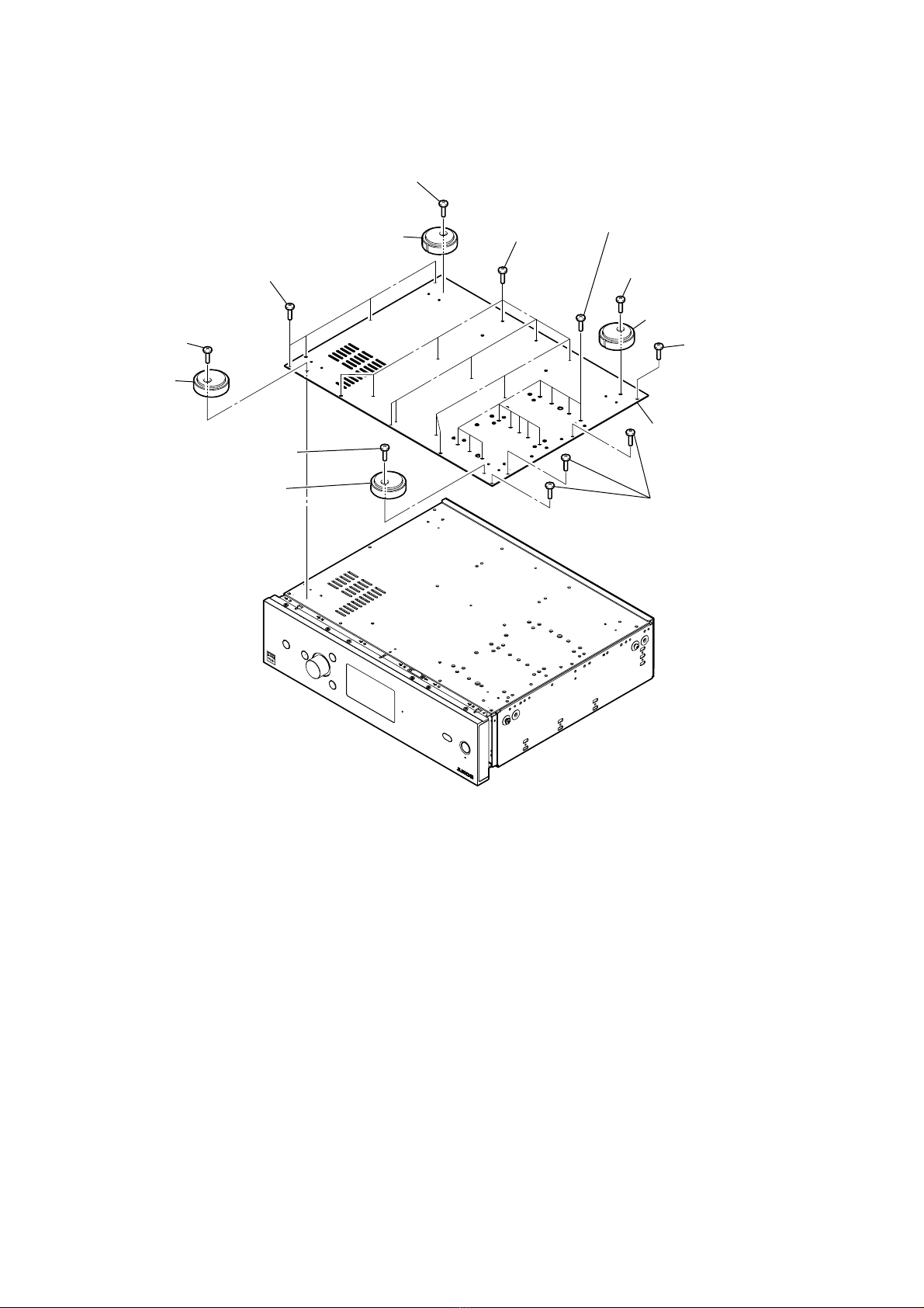
2-4. PLATE BOTTOM OUTER
1screw
(BVTT4 u20)
3twelve screws
(BVTT4 u8)
4three screws
(BVTP3 u8)
5plate bottom outer
4screw
(BVTP3 u8)
4twelve screws
(BVTP3 u8)
4four screws
(BVTP3 u8)
2foot assy
1screw
(BVTT4 u20)
2foot assy
1screw
(BVTT4 u20)
2foot assy
1screw
(BVTT4 u20)
2foot assy
– Bottom view –

HAP-Z1ES
9
2-5. PLATE BOTTOM, CABLE TIE
1Remove the plate bottom
in the direction of an arrow.
2plate bottom
3Cut two cable ties.
Note: In reassembling, use new cable tie
to fasten the clamp same as before.
cable tie cable tie
IO board
APOWER boardDCDC board
:LUHVHWWLQJ
–%RWWRPYLHZ–

HAP-Z1ES
10
2-6. FRONT PANEL BLOCK
2eight screws
(BVTP3 u8)
2two screws
(BVTP3 u8)
2screw
(BVTP3 u8)
3lug wire
4two brackets (panel)
– Bottom view –
1flexible flat cable (40P)
(CN703)
5Remove the front panel block
in the direction of an arrow.
qs front panel block
6conector
8conector
(CN7013)
9conector
(CN7002)
0conector
(CN7003)
qa conector
(CN7003)
7Remove wires from the lead pin.
lead pin
U-COM board
KEY JOG board
SPIRITOSO-LCD board
:LUHVHWWLQJ
colored line
connector
flexible flat cable
Note: When installing the flexible flat cable,
ensure the colored line.
No slanting after insertion.

HAP-Z1ES
11
2-7. WLAN/BT COMBO CARD (WBC1)
2-8. U-COM BOARD
1coaxial cable
(U.FL connector)
[gray]
Coaxial cables (U.FL connector) are upward.
1coaxial cable
(U.FL connector)
[black]
2screw
(BVTP3 u8)
3claw
4claw
5WLAN/BT COMBO card
(WBC1)
WLAN/BT COMBO card
(WBC1)
:LUHVHWWLQJ
–)URQWSDQHOEORFNUHDUYLHZ–
2conector
(CN7008)
3conector
(CN7009)
1Remove the wire from three lead pins.
1Remove the wire from the lead pin.
lead pin
4screw
(BVTP3 u8)
4screw
(BVTP3 u8)
4two screws
(BVTP3 u8)
5U-COM board
U-COM boardKEY JOG board
:LUHVHWWLQJ
–)URQWSDQHOEORFNUHDUYLHZ–
U-COM board
SPIRITOSO-LCD board
POWER KEY board
lead pin
lead pin lead pin
:LUHVHWWLQJ
Note: When the WLAN/BT COMBO card (Ref. No. WBC1) and
coaxial (U.FL connector) cables (Ref. No. WR1, WR2) are
replaced, refer to “CHECKING METHOD OF NETWORK
CONNECTION” on page 5.

HAP-Z1ES
12
2-9. KEY JOG BOARD
2-10. SPIRITOSO-ANT-R BOARD
– Front panel block rear view –
3conector
(CN305)
7conector
(CN304)
1knob (jog) assy
4four screws
(BVTP3 u8)
4four screws
(BVTP3 u8)
4screw
(BVTP3 u8)
5lug wire
2accessory nut
6Remove the KEY JOG board
in the direction of an arrow.
8KEY JOG board
3coaxial cable (U.FL connector)
(WR2) [gray]
coaxial cable (U.FL connector)
(WR2) [gray]
Do not fold.
1two claws
:LUHVHWWLQJ
2Remove the SPIRITOSO-ANT-R board
in the direction of an arrow.
4SPIRITOSO-ANT-R board
SPIRITOSO-ANT-R board
ditch ditch screw hole screw holehook hook
SPIRITOSO-ANT-R board
–)URQWSDQHOEORFNUHDUYLHZ–

HAP-Z1ES
13
2-11. SPIRITOSO-ANT-L BOARD
2-12. SPIRITOSO-LCD BOARD
3coaxial cable (U.FL connector)
(WR1) [black]
coaxial cable (U.FL connector)
(WR1) [black]
Do not fold.
1two claws
:LUHVHWWLQJ
2Remove the SPIRITOSO-ANT-L board
in the direction of an arrow.
4SPIRITOSO-ANT-L board
SPIRITOSO-ANT-L board
–)URQWSDQHOEORFNUHDUYLHZ–
3plate (LCD)
2two screws
(BVTP3 u8)
1flexible flat cable (40P)
(FFC1) (CN001)
2screw
(BVTP3 u8)
5SPIRITOSO-LCD board
4LCD flexible board
(CN002)
– Front panel block rear view –
colored line
connector
flexible flat cable
Note: When installing the flexible flat cable,
ensure the colored line.
No slanting after insertion.

HAP-Z1ES
14
2-13. LED BOARD
2-14. LCD PANEL (LCD1)
2Remove the LED board in
the direction of an arrow.
4LED board – Front panel block rear view –
1screw
(BVTP3 u8)
3connector
(CN031)
5LCD cushion (A)
LCD cushion (A)
6LCD cushion (B)
LCD cushion (B)
bottom side
top side
Note: Attach to fit the corner.
$WWDFKHGSRVLWLRQRI/&'FXVKLRQ
–)URQWSDQHOEORFNUHDUYLHZ–
1three screws
(BVTP3 u8)
2two claws
3holder (LCD)
4Remove the LCD panel block
in the direction of an arrow.
7LCD panel
(LCD1)

HAP-Z1ES
15
2-15. HDD BLOCK
2-16. HDD (HDD1)
1harness (S-002)
2harness (S-004)
3connector
(CN51)
A
B
B
A
4screw
(BVTP3 u8)
4screw
(BVTP3 u8)
4two screws
(BVTP3 u8)
HDD
MAIN board
5Remove the HDD base block
in the direction of an arrow.
6HDD block
Note 1: Check that the harness (S-002)
is not twisted.
Note 2: Push the harness (S-002) from HDD
in the direction of an arrow as not to
touch the DC fan.
DC fan
:LUHVHWWLQJ
1two step screws
1two step screws
5HDD (HDD1)
4base HDD block
2base fan block
3two step screws
Note 2: No problem using the electric screwdriver
when installing or removing these screws.
When tightening screws, tighten the below
torque value.
tightening torque: .. Nm
3two step screws
Note 2: No problem using the electric screwdriver
when installing or removing these screws.
When tightening screws, tighten the below
torque value.
tightening torque: .. Nm
Note 1: When the hard disk drive (Ref. No. HDD1) is replaced, refer
to “NOTE OF REPLACING THE HARD DISK DRIVE (Ref.
No. HDD1)” on page 4.

HAP-Z1ES
16
2-17. POWER TRANSFORMER (T1, T2)-1
2Cut the cable tie.
Keep a distance.
2Cut the cable tie.
3clamp filter
(ferrite core)
(FC1)
cable tie
cable tie clamp filter
(ferrite core)
(FC1)
power transformer
(T2)
power transformer
(T1)
power transformer
(T1)
Note: In reassembling, use new cable tie
to fasten the clamp same as before.
1Remove wires from
three lead pins.
lead pin
lead pin
power transformer
(T2)
APOWER boardDCDC board
lead pin
:LUHVHWWLQJ
:LUHVHWWLQJ

HAP-Z1ES
17
2-18. POWER TRANSFORMER (T1, T2)-2
A
A
B
B
1conector
(CN1404)
2conector
(CN1501)
3conector
(CN902) 4conector
(CN903)
power transformer
(T2)
Twist the wire in the
direction of an arrow.
power transformer
(T1)
:LUHVHWWLQJ
5two screws
(BVTT4 u8)
5two screws
(BVTT4 u8)
5two screws
(BVTT4 u8)
5two screws
(BVTT4 u8)
6power transformer
(T1)
6power transformer
(T2)

HAP-Z1ES
18
2-19. FPGA DSP BOARD
5four screws
(BVTP3 u8)
7FPGA DSP board
FPGA DSP board
MAIN board longer side
AUDIO board
2connector
(CN103)
6connector
(CN401)
3ferrite core
(FC2)
ferrite core
(FC2)
4flexible flat cable (24P) (FFC2)
(CN506)
flexible flat cable (24P)
(FFC2)
1cushion
cushion
cushion
1cushion
colored line
connector
flexible flat cable
Note: When installing the flexible flat cable,
ensure the colored line.
No slanting after insertion.
shorter side
:LUHVHWWLQJ

HAP-Z1ES
19
2-20. MAIN BOARD BLOCK
2-21. MAIN BOARD
AB
AB
2connector
(CN601)
3connector
(CN201)
4connector
(CN701)
5connector
(CN1003)
1harness (S-002)
(CN1001)
6screw
(BVTP3 u8)
6screw
(BVTP3 u8)
6screw
(BVTP3 u8)
6screw
(BVTP3 u8)
7Draw out two wires.
8MAIN board block
1connector
(CN203)
2connector
(CN1002)
3three screws
(BVTP3 u8)
5three screws
(BVTP3 u8)
5screw
(BVTP3 u8)
5screw
(BVTP3 u8)
3three screws
(BVTP3 u8)
4base board FPGA
6base board main block
8MAIN board
7sheet radiation (20)
5screw
(BVTP3 u8)
Note: When the complete MAIN board is replaced, refer to
“NOTE OF REPLACING THE COMPLETE MAIN
BOARD” and “CHECKING METHOD OF NET-
WORK CONNECTION” on page 5.

HAP-Z1ES
20
2-22. APOWER BOARD
1Cut the cable tie.
Note: In reassembling, use new cable tie
to fasten the clamp same as before.
2Remove wires from
four lead pins.
3connector
(CN1502)
4connector
(CN151)
lead pin
lead pinlead pin
lead pin cable tie
APOWER board
IO board
DCDC board
AUDIO board
:LUHVHWWLQJ
6screw
(BVTP3 u8)
7APOWER board
6screw
(BVTP3 u8)
6three screws
(BVTP3 u8)
5connector
(CN102)
Other manuals for HAP-Z1ES
7
Table of contents
Other Sony Turntable manuals

Sony
Sony MDX-C8900 User manual

Sony
Sony AIVA AZ-BS1 User manual

Sony
Sony PS-J10 Primary User manual

Sony
Sony PS-LX300H User manual

Sony
Sony Walkman WM-EX162 User manual

Sony
Sony PS-DJ9000 - Stereo Turntable System User manual

Sony
Sony Betacam SX DNW-A22 User manual

Sony
Sony PS-FL7II - Stereo Turntable User manual

Sony
Sony MDX-C670 User manual

Sony
Sony HAP-Z1ES User manual