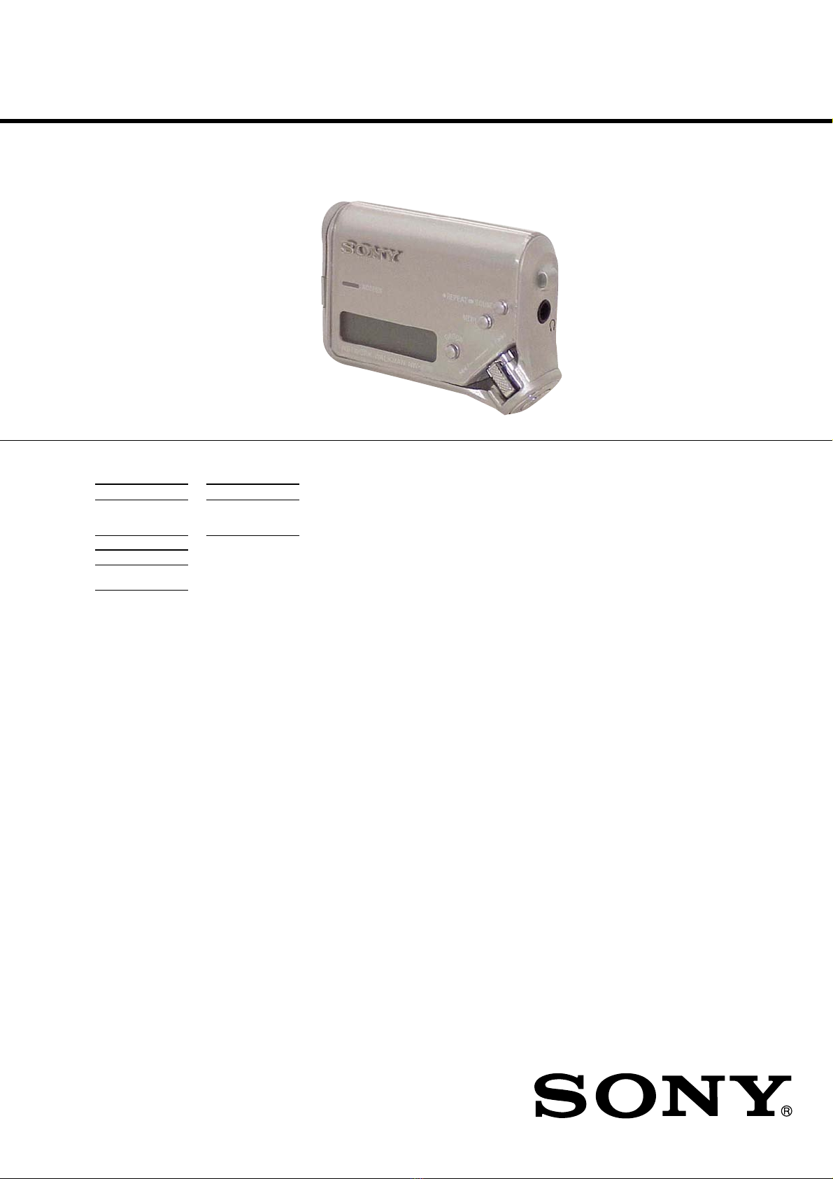
Sony NW-E99 - Network Walkman User manual

SERVICE MANUAL
Sony Corporation
Connect Company
Published by Sony Engineering Corporation
US Model
Canadian Model
AEP Model
E Model
Tourist Model
PORTABLE IC AUDIO PLAYER
9-879-316-06
2005I16-1
© 2005.09
Ver. 1.5 2005.09
SPECIFICATIONS
NW-E99
Sampling frequency
ATRAC3, ATRAC3plus, MP3: 44.1 kHz
Audio compression technology
Adaptive Transform Acoustic Coding3 (ATRAC3)
Adaptive Transform Acoustic Coding3plus
(ATRAC3plus)
MPEG1 Audio Layer-3 (MP3): 8 to 320 kbps,
variable bit rate-compliant
Frequency response
20 to 20,000 Hz (single signal measurement)
Output
Headphone: Stereo mini-jack
Supplied accessories
Headphones (1)
Dedicated USB cable (1)
Carrying pouch (1)
Neck strap (1)
Extension headphone cord (1)
CD-ROM for the SonicStage software (1)
Operating Instructions (1)
SonicStage Operating Instructions (1)
CD-ROM for the Operating Instructions and
SonicStage Operating Instructions (1)
Design and specifications are subject to
change without notice.
US and foreign patents licensed from Dolby
Laboratories.
Dynamic range
85 dB or more (excluding ATRAC3 66 kbps)
Operating temperature
5˚C to 35˚C (67˚F to 95˚F)
Power source
Size AAA (LR03) alkaline battery
Battery life (continuous
playback)
ATRAC3 format: Approximately 70 hours
(Playback at 105 kbps)
ATRAC3plus format: Approximately 60 hours
(Playback at 48 kbps)
MP3 format: Approximately 50 hours
(Playback at 128 kbps)
Dimension
56 ×37.3 ×15 mm (2 1/4×1 1/2×19/32 inches)
(w/h/d, projecting parts not included)
Mass
Approx. 40 g (2 oz) (battery not included)
Signal-to-noise ratio (S/N)
80 dB or more (excluding ATRAC3 66 kbps)
* The values for ATRAC3, ATRAC3plus apply if
the MP3 File Manager software has been erased
from the built-in flash memory.
ATRAC3plus*
8 hr. 00 min. (256 kbps)
34 hr. 20 min. (64 kbps)
46 hr. 40 min. (48 kbps)
ATRAC3*
16 hr. 40 min. (132 kbps)
21 hr. 00 min. (105 kbps)
33 hr. 40 min. (66 kbps)
MP3
8 hr. 00 min. (256 kbps)
16 hr. 00 min. (128 kbps)

2
NW-E99
TABLE OF CONTENTS
1. GENERAL ................................................................... 3
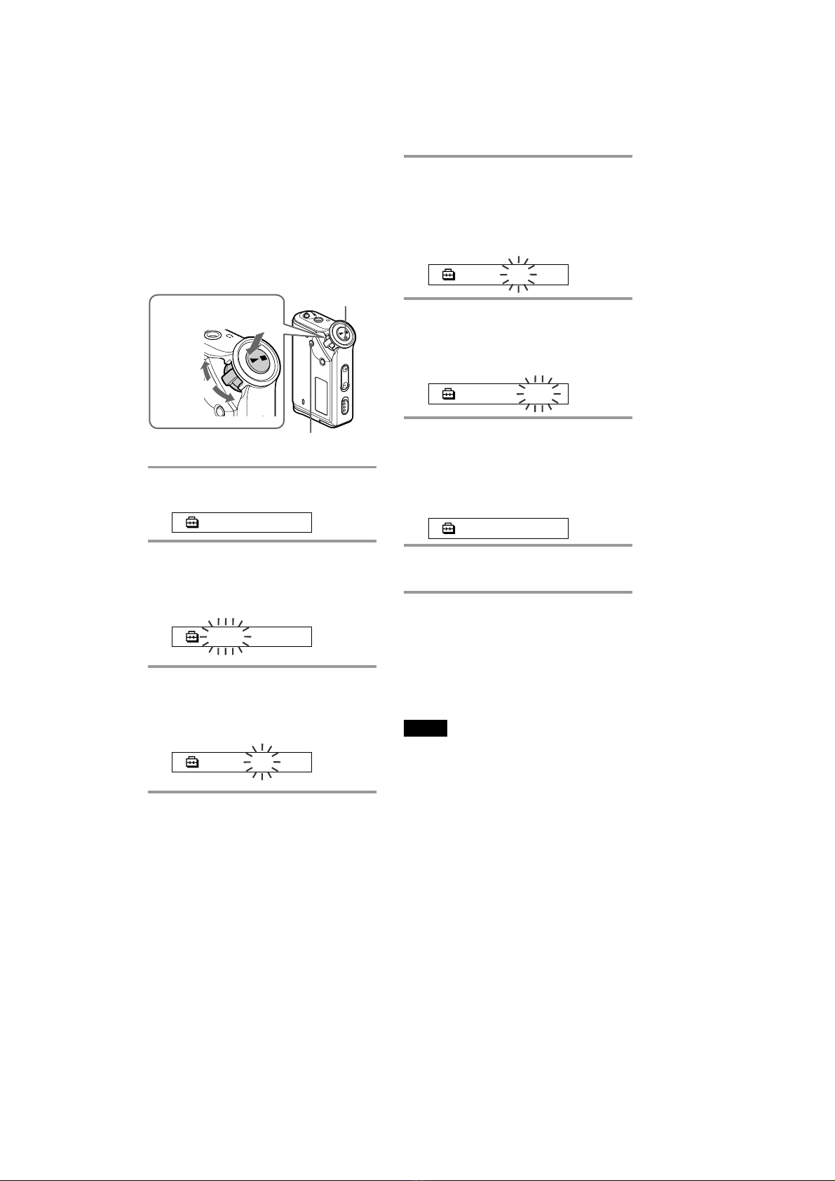
2. TEST MODE ............................................................... 5
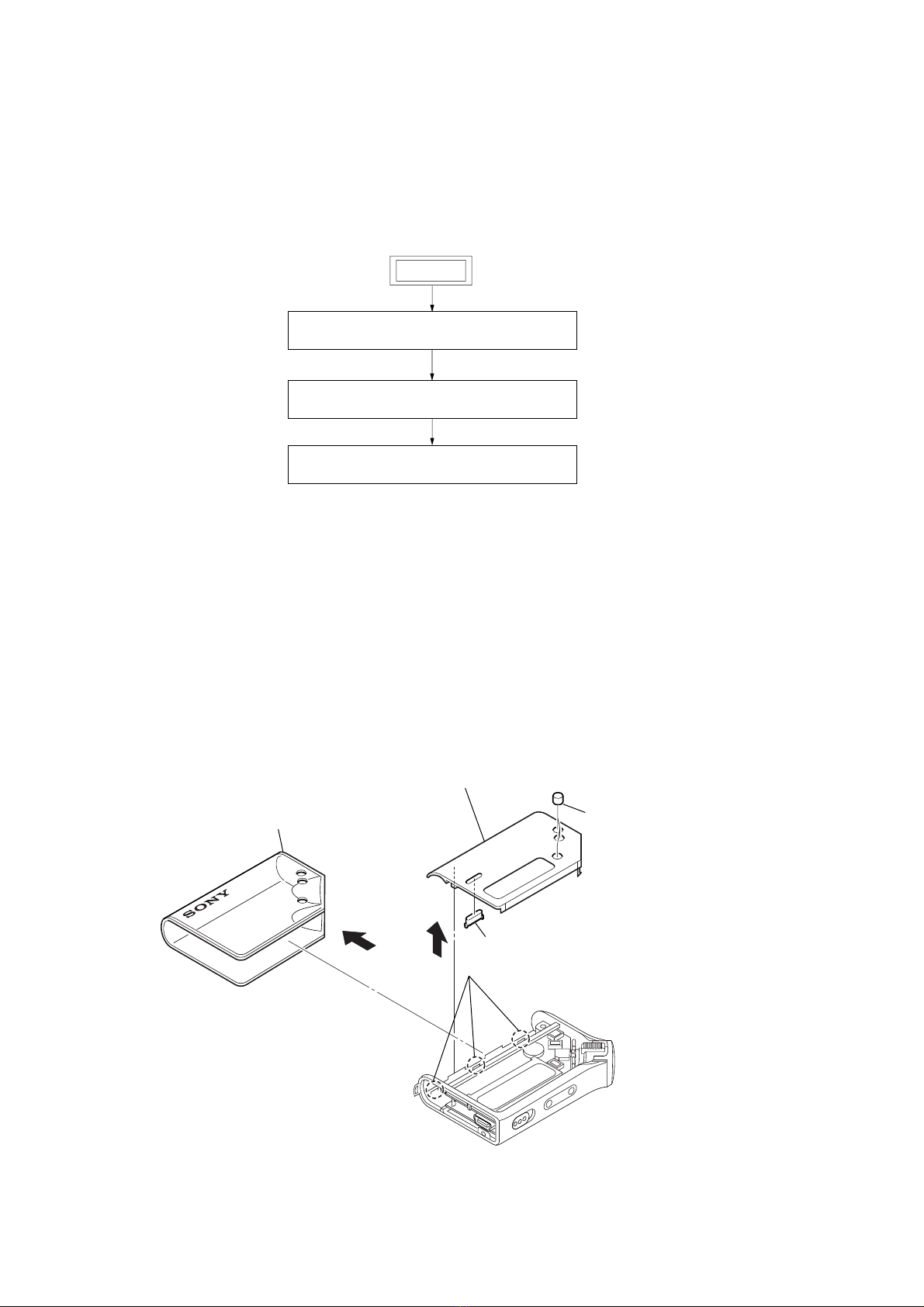
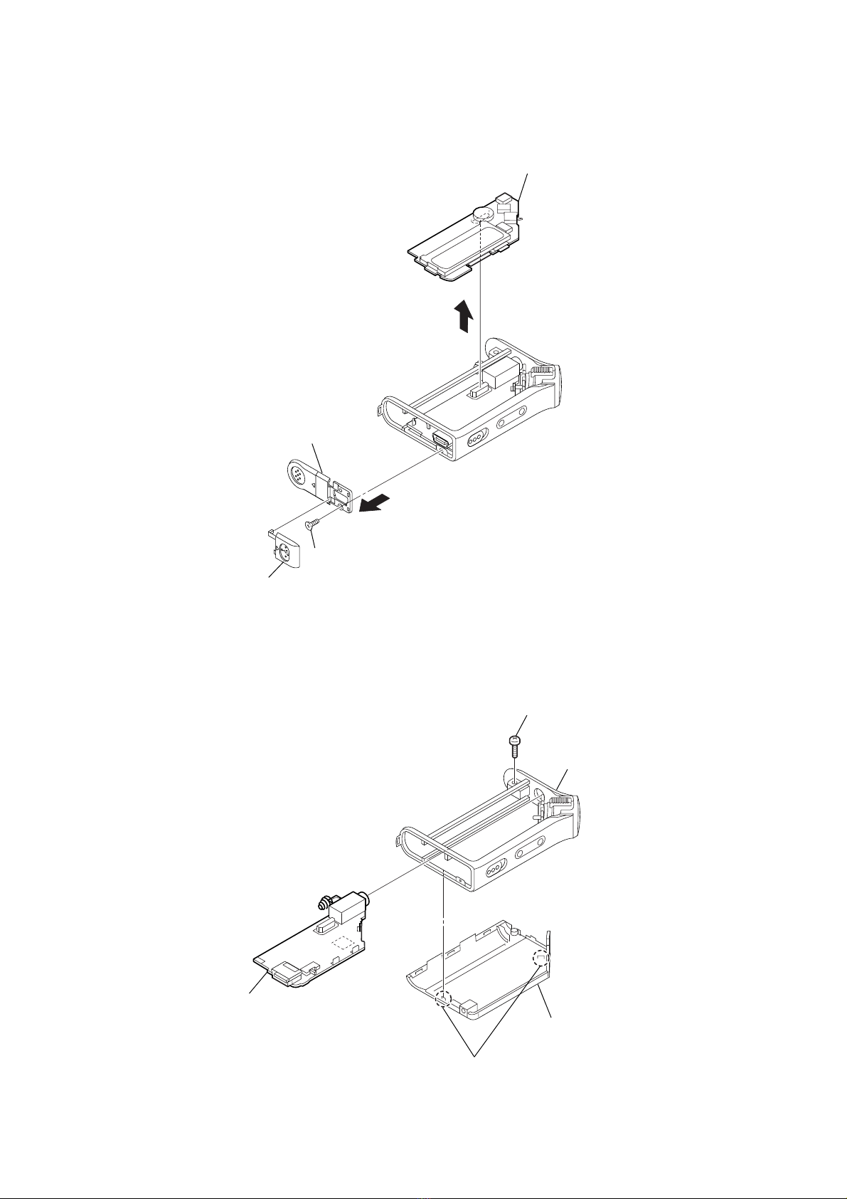
3. DISASSEMBLY
3-1. Case, Chassis (Front) Assy .............................................. 6
3-2. DISPLAY Board Assy ..................................................... 7
3-3. MAIN Board Assy ........................................................... 7
4. DIAGRAMS
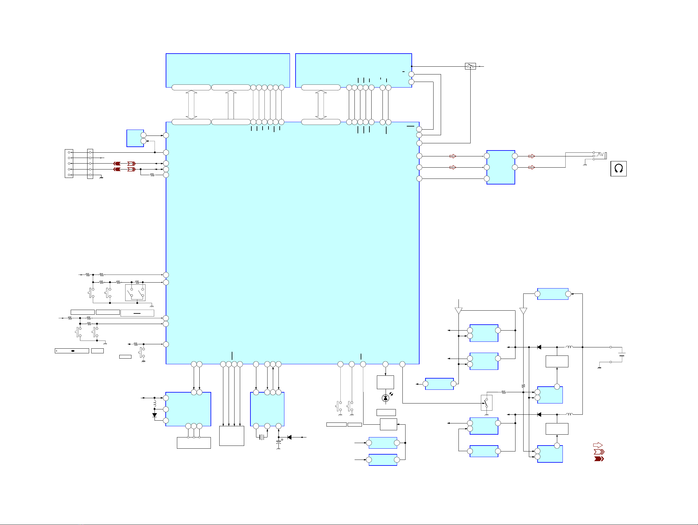
4-1. Block Diagram ................................................................ 9
4-2. Printed Wiring Board
– DISPLAY Board (Side A) – ......................................... 10
4-3. Printed Wiring Board
– DISPLAY Board (Side B) – ......................................... 11
4-4. Schematic Diagram – DISPLAY Board – ....................... 12
4-5. Printed Wiring Board – MAIN Board (SideA) –............ 13
4-6. Printed Wiring Board – MAIN Board (Side B) –............ 14
4-7. Schematic Diagram – MAIN Board (1/2) – .................... 15
4-8. Schematic Diagram – MAIN Board (2/2) – .................... 16
5. EXPLODEDVIEWS
5-1. Overall Assy Section ....................................................... 18
5-2. MAIN Board Section....................................................... 19
6. ELECTRICAL PARTS LIST .................................. 20
Microsoft, Windows and Windows Media are trademarks or
registered trademarks of Microsoft Corporation in the United States
and/or other countries.
US and foreign patents licensed from Dolby Laboratories.
All other trademarks and registered trademarks are trademarks or
registered trademarks of their respective holders.
UNLEADED SOLDER
Boards requiring use of unleaded solder are printed with the lead-
free mark (LF) indicating the solder contains no lead.
(Caution: Some printed circuit boards may not come printed with
the lead free mark due to their particular size)
: LEAD FREE MARK
Unleaded solder has the following characteristics.
•Unleaded solder melts at a temperature about 40 °C higher
than ordinary solder.
Ordinary soldering irons can be used but the iron tip has to be
applied to the solder joint for a slightly longer time.
Soldering irons using a temperature regulator should be set to
about 350 °C.
Caution: The printed pattern (copper foil) may peel away if
the heated tip is applied for too long, so be careful!
•Strong viscosity
Unleaded solder is more viscou-s (sticky, less prone to flow)
than ordinary solder so use caution not to let solder bridges
occur such as on IC pins, etc.
•Usable with ordinary solder
It is best to use only unleaded solder but unleaded solder may
also be added to ordinary solder.
•IC400 (microcomputer) and IC450 (nor flash sram) on MAIN
board cannot be replaced individually.
Replace it with MAIN board assembly for service.
Flexible Circuit Board Repairing
•Keep the temperature of the soldering iron around 270 °C
during repairing.
•Do not touch the soldering iron on the same conductor of the
circuit board (within 3 times).
•Be careful not to apply force on the conductor when soldering
or unsoldering.
Notes on chip component replacement
•Never reuse a disconnected chip component.
•Notice that the minus side of a tantalum capacitor may be
damaged by heat.

3
NW-E99
SECTION 1
GENERAL This section is extracted
from instruction manual.
Locating controls
Rear sideFront side
7Headphone jack
8Nx button
0VOLUME +/– button
qa HOLD (Locking controls) switch
qs USB jack
qd Battery compartment
G
r
o
u
p
M
o
d
e
1
2
3
4
5
6
7
8
9
0
qz
OPEN
qs
qd
1Strap hole for attaching the strap
2REPEAT/SOUND button
3MENU button
You can switch to the Time display by
pressing the MENU button for a while.
4GROUP button
5Display
6ACCESS lamp
9Shuttle switch

4
NW-E99
4As you did in step 3, adjust the settings
for “month” and “date.”
After rotating the Shuttle switch to adjust the
“date” setting and pressing the Nx button
to confirm, the display switches to the time
setting screen.
0:00
5Rotate the Shuttle switch to adjust the
“hour” setting and press the Nx
button to confirm.
The “minute” digit blinks.
0:00
6As you did in step 5, adjust the settings
for “minute.”
After rotating the Shuttle switch to adjust the
“minute” setting and pressing the Nx
button to confirm, the display switches to the
time setting screen.
DA
T
E-
T
IME
7Press the MENU button.
The display returns to the normal screen.
Select [RETURN] in the menu screen or press the MENU
button.
Press the MENU button and hold it.
You can display the current time while pressing the
button.
Notes
• If the unit is not used for a long time, your settings of
the date and time may be reset.
• If the current time is not set, the display for the date and
time will be “-- --.”
• If PC CLK is set to “ON”, the time setting of your
Network Walkman is automatically adjusted to a
computer’s built-in clock when your Network Walkman
is connected to the computer.
• Depending on the shipping area, the time display
format of the unit is set to a 12-hour display or a 24-
hour display.
You cannot switch between a 12-hour display and a 24-
hour display in the unit.
A 24-hour display is shown in this manual.
To cancel the menu mode
To display the current time
Adjusting the
current time
setting (DATE-
TIME)
You can set and display the current time.
1Press the MENU button.
The menu screen is displayed.
REPEAT MODE
>
2Rotate the Shuttle switch to select
“DATE-TIME” and press the Nx
button to confirm.
The “year” digit blinks.
2004y 1m 1d
3Rotate the Shuttle switch to adjust the
“year” setting and press the Nx
button to confirm.
The “month” digit blinks.
2004y 1m 1d
G
r
o
u
p
M
o
d
e
o
d
e
Shuttle switch Press
(Confirm)
Nx button
MENU button
to (+/>)
to (./–)

5
NW-E99
SECTION 2
TEST MODE
STANDING PROCEDURE
Procedure 1: Set a dry battery into NW-E99, and keep the battery
lid open.
Procedure 2: In HOLD state, while pushing Nx and [GROUP]
button, turn power on by closing the battery lid of
NW-E99.
Procedure 3: Set HOLD state off.
After starting up test mode, the following contents can be checked.
TEST MODE
• Nx button
The KEY test mode is activated. All key inputs are completed,
then Nx button is pressed, restart. (Be aware that the
initialization is included on all key input.)
• [MENU] button
EL0 (blue) lights on/off.
• [GROUP] button
EL1 (green) lights on/off.
• -/>
All LCD lights and ACCESS LED lights off.
• ./+
All LCD lights and ACCESS LED lights on.
• [VOL +] button
BEEP turns on.
• [VOL --] button
BEEP turns off.
• [ REPEAT SOUND] button
Initialized. (Turns to the factory preset state, time, volume setting
and so on.)
The music data, files and so on in the memory are not changed.
•

6
NW-E99 SECTION 3
DISASSEMBLY
Note: Follow the disassembly procedure in the numerical order given.
Note: Disassemble the unit in the order as shown below.
3-1. CASE, CHASSIS (FRONT) ASSY
SET
3-1. CASE,CHASSIS (FRONT) ASSY
(Page 6)
3-2. DISPLAY BOARD ASSY
(Page 7)
3-3. MAIN BOARD ASSY
(Page 7)
1
case
3
chassis (front)
4
three button (cup)
5
window (led)
2
three claws

7
NW-E99
3-2. DISPLAY BOARD ASSY
3-3. MAIN BOARD ASSY
4
DISPLAY board ass
y
2
tapping screw (1.7)
3
cover section
1
lid (usb) (sub assy)
4
MAIN board assy
3
chassis (rear)
ornament assy
2
two claws
1
tapping screw (B1.7
×
7
)

8
NW-E99 SECTION 4
DIAGRAMS
Note on Schematic Diagram:
•All capacitors are in µF unless otherwise noted. (p: pF) 50 WV or
less are not indicated except for electrolytics and tantalums.
•All resistors are in Ωand 1/4W or less unless otherwise specified.
•%: indicates tolerance.
•C: panel designation.
•: B+ Line.
•Power voltage is dc 1.5 V and fed with regulated dc power supply
from battery terminal.
•Voltages and waveforms are dc with respect to ground under no-
signal (detuned) conditions.
no mark : PLAY
•Voltages are taken with a VOM (Input impedance 10 MΩ).
Voltage variations may be noted due to normal production toler-
ances.
•Waveforms are taken with a oscilloscope.
Voltage variations may be noted due to normal production toler-
ances.
•Circled numbers refer to waveforms.
•Signal path.
F: PLAY
a: DIGITAL OUT
k: DIGITAL IN
Note on PrintedWiring Board
• X: parts extracted from the component side.
• Y: parts extracted from the conductor side.
• : Pattern from the side which enables seeing.
•:Through hole.
Caution:
Pattern face side: Parts on the pattern face side seen from
(Side A) the pattern face are indicated.
Parts face side: Parts on the parts face side seen from
(Side B) the parts face are indicated.
•Waveform
1
IC700 8(OSCOUT)
0.5 V/div, 10
µ
sec/div
1.1 Vp-p
31.25
µ
sec

99
NW-E99
NW-E99
4-1. BLOCK DIAGRAM
VBUS DET
IC506
NOR FLASH SRAM
IC450
NAND FLASH RAM
IC461
CN400
STAND
CONNECTOR
USB
CONNECTOR
VIN
VOUT
2
1
2
3
4
5
5
126
38 - 53
185
197 - 207, 2 - 9
187 184 183 186 182
23 24 26 28 27 30 29
15 - 22
29 - 32, 41 - 4429 - 36, 38 - 45 111 - 8, 16 - 25, 48 13 14 15 26 28 16 17 18 19 8 7 9
128
129
130
102
104
83
176
60 57 58 76 74 75 73
7432
8910
87 81
106
41
5
3
3
5
2
3
5
2
1
1
5
2
1
5
3
2
14
4
41
172
59
84
133
134
174
7
8
3
9
2
127
+5VDC
DATA -
DATA +
GND
VBUS
VDIOUS
UDM
UDP
TRON
VBUS
D-
+5V
D+
USB GND
AN4
AN6/INT8
S703
VOLUME - S702 S701
VOLUME +
S707
PF2/INT4
VDD
VDD
VOUT
VOUT
VOUT
VOUT
CE
VDD
VDD
CE
VIN
VOUT
CE
VIN
VOUT
VOUT
CE
VIN
VOUT
CE
VIN
IN1
2.8V
Q460
OUT1
IN2
STB
OUT2
VOUT VDD
OSCOUT
XRST
XCS
SCL
SDA
OSCIN
VDD
CE
SI
SO
SCLK
+2.8V
+2.3V
PI5
PC3
SCK0
SO0
PE7
AN3
SO1
SI1
SCK1
AN2
AN1
PG1/INT5
PFO/INT3
RST
PI1
PC2
PF3
AOUTR
AOUTL
PI3
VCC
XSTBY
FCE0
FRB0
FCLE
FAD0 - 7A1 - 19D0 - 15
FRE
FWP
FWE
FALE
CSI
WE
RE
CS0
LB
UB
CE
R/B
CLE
I/O1 - 8A1 - 19DQ0 - 15
RE
WP
WE
ALE
BES
WE
OE
BEF
LBS
UBS
LIQUID
CRYSTAL
DISPLAY
CLOCK
OSC
IC700
SYSTEM CONTROLLER
IC400
D703
X700
32kHz
S706
HOLD
.
S708
GROUP
CORE DET
IC502
+1.2V REG.
IC504
CORE SW
IC501
14
VOUT VDD
I/O DET
IC510
+2.8V REG.
IC508
+VIO
+1.4V
+1.2V
+2.8V
+2.3V
+2.8V
+1.2V
+2.8V
+2.8V
IC500
Q503
+1.2V
Q506, 507
Q501
J301
HP AMP
IC301
+2.3V REG.
IC509
D501
• SIGNAL PATH
: PLAY BACK
: DIGITAL OUT
: DIGITAL IN
L500
L501D504
SWITCHING
Q500
SWITCHING
Q505
SWITCHING
REG.
IC507
SWITCHING
REG.
IC503
I/O DET
IC505
RESET
Q502, 504
LED
DRIVER
Q701
D702
ACCESS
103
105
AN5
AN7/INT9
S705
REPEAT SOUND
S704
MENU
+2.3V
DRY
BATTERY
SIZE "AAA"
(IEC DESIGNATION LR03)
1PC, 1.5V
Nx
>.
/- /+
MEMORY STICK INTERFACE
MAGIC GATE CORE
NAND FLASH INTERFACE
USB INTERFACE
A/D, D/A CONVERTER
SERIAL INTERFACE
LEVEL BATTERY DETECT
160 173
10
13
1
20
11
1518 16
VDD
LDR
CHV
PR4
PI2
OUT2
OUT1
OUTCM
ENA2
ENA1
+2.8V
L801
D801
EL ELEMENT
IC801
EL DRIVER
32
31
FCE1
FRB1
6
R/B1
10
CE1

1212
NW-E99
NW-E99
4-4. SCHEMATIC DIAGRAM – DISPLAY BOARD – •See page 17 for IC Block Diagram.
801
EL DRIVER
D702
R713
R708
R706
SL700
R710
TP706
D703
TP806
TP853
TP401
TP850
TP851
TP701
TP705
S701
R700
R701
S704
R704
C702
TP804
TP852
TP410
S708
S705
C522
TP805
Q701
CN402
24P
C700
SML-512DWT86
100
47k
100k
BATTERY
(BACK-UP)
(SECONDARY)
1k
VDD_RTC
RB520S-30TE61
CN850
20P
VDD
LCDDA
EL1
LCDRST
LCD_A0
LCDCS
ADK2
GROUP
47k
22k
22k
100p
VDD_EL
LCDCK
EL2
1
GND
2SC5658T2L
R850 100k
R851
100k
R852
R860 0
R862 0
R865 0
R866 0
R861 0
0
R863 0
R864 0
C860 1
C867 1
C866 1
C861 0.47
C862 0.47
C863 0.47
C864 0.47
C865 0.47
VDD
12
IC801
C802
D801
L801
R801
R805
R802
R803
R804
C801
SM8145AB-G-EL
4700p
1SS403(TPH3)
100k
150k
33k
47k
33k
0.01
Ver. 1.1

1313
NW-E99
NW-E99
IC461
*IC400
*IC450
*CSP
(Chip Size Package)
*CSP
(Chip Size Package) IC301
1-862-328- (31)
31
MAIN BOARD (SIDE A)
4-5. PRINTEDWIRING BOARD – MAIN BOARD (SIDE A) – :Uses unleaded solder.
• Semiconductor
Location
Ref. No.
Location
D300 C-6
IC301 C-7
IC400 C-3
IC450 D-2
IC461 C-5
✩IC400 (microcomputer) and IC450 (nor flash sram) on MAIN
board cannot be replaced individually.
Replace it with MAIN board assembly for service.

1414
NW-E99
NW-E99
IC506
IC503
IC507
IC500
IC700
IC508
IC504
IC501
IC502
IC505
IC510
IC509
(
S707
S702
VOLUME
+
S703
VOLUME
-S703
OFF ON
HOLD
1
1
5
3
5
4
12
34
1
3
5
4
4
5
3
1
5
4
1
1
1
1
1
3
5
4
2
34
12
34
23
43
54
3
12
34
1
2
23
24
2
1-862-328- (31)
31
MAIN BOARD (SIDE B)
DRY BATTERY SIZE "AAA"
(IEC DESIGNATION LR03)
1PC, 1.5V
DISPLAY BOARD
CN402
(Page 10)
A
4-6. PRINTEDWIRING BOARD – MAIN BOARD (SIDE B) –
:Uses unleaded solder.
•Semiconductor Location
Ref. No.
Location
D501 B-6
D502 C-8
D503 C-8
D504 C-6
IC500 D-8
IC501 B-4
IC502 C-4
IC503 C-6
Ref. No.
Location
IC504 B-5
IC505 D-4
IC506 C-8
IC507 D-7
IC508 C-5
IC509 B-3
IC510 D-2
IC700 D-5
Ref. No.
Location
Q460 C-3
Q500 B-6
Q501 D-7
Q502 B-3
Q503 D-8
Q504 B-3
Q505 D-6
Q506 C-3
Q507 C-4

1515
NW-E99
NW-E99
4-7. SCHEMATIC DIAGRAM – MAIN BOARD (1/2) – •See page 17 for IC Block Diagram. •See page 8 for Waveform. ✩IC400 (microcomputer) on MAIN board cannot be replaced
individually.
Replace it with MAIN board assembly for service.
*
*
C404
C405
C400
R720
R422
TP407
C418
TP402
TP403
TP404
TP405
VDR401
TP408
TP411 R420
TP416
TP417
TP415
TP418
VDR402
C421
C419
TP409
C414
C415
C417
R412
X401
R411
R409
C411
C408
R408
R407
R406
R405
R403
C406
C407
R402
C403
C402
VDR404
VDR403
R719 C709
R705
Q460
R724
VDR701
R718
R717
R711
R703
S702
R702
TP700
R721 TP704 VDR700
R725
R723
R709 TP702
C701TP412
R416
C704
C705
C706
R400
VDR400
C401
TP406
R401
R722
TP701
C707
X700
IC700
R461
R4650
R4660
R415100K
C462
VDR405
R716
R715
R463
R726
S706
C703
R410
R453
C464
R462
IC461
K04SONY99
S707
S703
R714
C416
R404
CN401
24P
X400
R421
C409
C410
0.1
0.1
0.1
0
10k
PD4
0.1
TXD0
TXD0
TXD0
TXD0
MSINS
MSDIS 10k
MSSCLK
MSBS
MSPWR
XMS
0.1
0.1
XBOOT
0.1
10p
0.1
220
16MHz
1M
22
1
1
1.5k
22
22
0
2.2M
1000p
0.1
10k
4.7
10V
4.7
10V
10k 0.1
470k
NDS356AP
10k
22k
10k
10k
1k
10k
ADK1
10k XHOLD
470k
470k
10k XPLAY
0.01
DEBUG
100k
0.01
0.01
0.01
1M
1000p
RST
10k
470k
VDDRTC
0.1
32.768KHz
RS5C348A-E2-FB
100k
0.1
10k
10k
100k
0
1000p
100
470k
1
1k
22k
10p
470k
22MHz
100k
0.1
4.7
6.3V
Ver. 1.5

1616
NW-E99
NW-E99
4-8. SCHEMATIC DIAGRAM – MAIN BOARD (2/2) – •See page 17 for IC Block Diagram. ✩IC450 (nor flash sram) on MAIN board cannot be replaced
individually.
Replace it with MAIN board assembly for service.
IC301
C104
R103
R102
R203
C204
C103
C305 C303 R101 C102
C100
R200
C200
C202
R201
R302
C301
R300
C203
TP208
TP108
R533
TP509
C520
TP414
TP314
TP503
R531
R532
D504
TP506
C518
R530
R528
R526
R523
Q506
C511
R527
R529
TP505
C516
C512
R519
R510
Q502
R502 C503
R507
R522
R501
R505
R514
TP508
Q501
IC500
D503
D502
C513
C515
R513
R508
R500
D501
R518
R516
R511
R506
R509
R504
TP502
C506
C505
R512
R521R515
R520
C508
C501
TP501
TP500
TP507
J301
C304
C101
C201
C300
D300
C302
IC509
C521
VDR502
IC508
IC504
L501
IC507
Q505
C517
Q507
C519
Q504
C509
C502
0.1
VDR504
IC503
Q503
C504
L500
VDR501
VDR503
C500
VDR500
R450
C450
R451
R452
R202
TP504
R303
IC506
R524
IC501
Q500
IC505
R517
IC502
FB200
FB100
FB300
R100
FB302
R503
R525
C510
CN400
NJM2776RB2 (TE2)
0.22
47k
33k
47k
0.22
100p
0.1 0.33 10 0.22
0.022
4.7k
0.022
0.22
10
47k
0.1
0
100p
HP-R
HP-L
0
2.3V
0.1
D-
D+
1.2V
0
0
R534
100
RSX101M-30TR
33p
470k
100k
100k
470k
2SC5658T2L
0.047
470k
1M
REGCE
0.1
0.01
1M
470k
2SC5658T2L
1M 0.022
470k
47K
100k
2.2M
470k
VCORE
3LN01S-K-TL-E
S-80809CNPF-B9N-TF
1SS400TE-61
1SS400TE-61
0.1
10
47k
220k
470k
RSX101M-30TR
1M
470k
220k
330k
2.2M
2.2M
NM
1
0.1
100k
470k220k
22k
0.1
1
BATT+
BATT-
2.8V
10
10V
220
2.5V
220
2.5V
10
10V
MAZS120008SO
22
4V
XC62HR2301MR
4.7
6.3V
XC62HR2802MR
R1160N121B-TR-FA
XC9105D091MR
XP151A13A0MR
47
10V
2SA2029T2L
100
6.3V
2SA2029T2L
10
6.3V
XC9105D091MR
XP4601
47
10V
47
10V
0
0.1
100k
100k
33k
VBUS
0
XC62HR3302MR
1M
S-80810CNPF-B90-TF
XP151A12A2MR
S-80824CNBB-B8J-TF
IC510
S-80824CNPF-B8J-TF
100k
S-80810CNPF-B90-TF
4.7k
1M
1M
47p
5P

17
NW-E99
•IC Block Diagrams
IC301 NJM2776RB2 (TE2)
1
2
3
4
5
10
9
6
7
V+2O
OUT1
IN1
STANDBY
V+1VREF
OUT2
GND
STANDBY
8IN2
BIAS
REG
IC700 RS5C348A-E2-FB
VDD
VDD
OSCIN
OSCOUT
CE
INTR
32KOUT
SCLK
SO
SI
VSS
32 kHz
OUTPUT
CONTROL COMPARATOR
W
COMPARATOR
D
ADDRESS
REGISTER
I/O
CONTROL
ADDRESS
DECODER
SHIFT
REGISTER
INTERRUPT
CONTROL
OSC
DETECT
VOLTAGE
DETECT
ALARM W REGISTER
(WEEK, MIN, HOUR)
ALARM D REGISTER
(MIN, HOUR)
DIV OSC
DIVIDER
CORRECTION
9
10
8
7
6
2
3
4
5
1
TIMER COUNTER
SEC, MIN, HOUR, WEEK,
DAY, MONTH, YEAR
– MAIN Board –
IC801 SM8145AB-G-EL
– DISPLAY Board –
LDR
NC
NC
OCL1
OCL2
NC
OCL3
OCE
ENA2 ENA1
NC
VDD
NC
OUT2
OUT1
NC
NC
CHV
OUTCOM
VSS
20 19 18 17 16 15 14 13 12 11
12345678910
OSCILLATOR OSCILLATOR
DIVIDER
DIVIDER
CONTROL
LOGIC
HIGH VOLTAGE SWITCHING
CIRCUIT

18
NW-E99
74-984-017-11 SCREW (1.7), TAPPING
83-266-597-11 COVER (USB)
9X-3385-162-1 TERMINAL (+) SUB ASSY, BATTERY
10 3-266-599-11 LID, BATTERY CASE
11 3-247-180-01 SCREW (1.4X3)
12 X-2050-990-1 LID (USB) SUB ASSY
SECTION 5
EXPLODEDVIEWS
NOTE:
•-XX and -X mean standardized parts, so they
may have some difference from the original
one.A
•Items marked “*” are not stocked since they
are seldom required for routine service.
Some delay should be anticipated when
ordering these items.
•The mechanical parts with no reference
numberin the exploded views arenot supplied.
Ref. No. Part No. Description Remark
13-266-585-42 CASE
22-342-339-61 CHASSIS (FRONT)
33-266-591-11 BUTTON (CAP)
43-266-592-01 WINDOW (LED)
53-267-336-01 SHEET (BUTTON), ADHESIVE
63-266-596-11 LID (USB)
5-1. OVERALL ASSY SECTION
1
2
4
6
7
10 11
9
8
3
12
not supplied
main board sectio
n
5
Ref. No. Part No. Description Remark
Ver. 1.4

19
NW-E99
Ref. No. Part No. Description Remark Ref. No. Part No. Description Remark
51 3-318-203-81 SCREW (B1.7X7), TAPPING
52 3-266-604-21 ORNAMENT
53 3-266-584-11 BUTTON (PLAY)
54 3-266-608-01 SHEET (COVER), ADHESIVE
55 3-266-586-11 COVER (PLAY)
56 3-266-581-11 KNOB (HOLD)
57 2-023-871-01 SHEET (VOL), ADHESIVE
58 3-266-582-11 BUTTON (VOL)
59 3-266-595-01 SHEET (VOL)
60 2-048-634-01 SHEET (FRONT), ADHESIVE
5-2. MAIN BOARD SECTION
51
54 55
53
56
57
58
62
63 64 67
65 66
68
52
69
60
61
59
61 2-342-341-31 CHASSIS (REAR)
62 X-2102-785-1 MAIN BOARD, COMPLETE
63 3-266-606-01 SHAFT (PLAY)
64 3-266-583-01 ARM (SHUTTLE)
65 3-266-588-01 INNER (SHUTTLE)
66 3-266-610-01 KNOB (SHUTTLE)
67 3-266-605-01 SPRING (SHUTTLE)
68 A-1095-905-A DISPLAY BOARD, COMPLETE
69 2-048-635-01 SHEET (REAR), ADHESIVE
Ver. 1.5

20
NW-E99 SECTION 6
ELECTRICAL PARTS LIST
NOTE:
•Due to standardization, replacements in the
parts list may be different from the parts
specified in the diagrams or the components
used on the set.
•-XX and -X mean standardized parts, so they
may have some difference from the original
one.
•RESISTORS
All resistors are in ohms.
METAL: Metal-film resistor.
METAL OXIDE: Metal oxide-film resistor.
F: nonflammable
•Items marked “*” are not stocked since they
are seldom required for routine service.
Some delay should be anticipated when
ordering these items.
•SEMICONDUCTORS
In each case, u: µ, for example:
uA. . : µA. . uPA. . : µPA. .
uPB. . : µPB. . uPC. . : µPC. .
uPD. . : µPD. .
•Accessories are given in the last of this parts
list.
Ref. No. Part No. Description Remark Ref. No. Part No. Description Remark
A-1095-905-A DISPLAY BOARD, COMPLETE
************************
1-805-081-12 ELEMENT, EL
1-805-082-11 DISPLAY PANEL, LIQUID CRYSTAL
2-024-570-01 SPACER (JACK)
2-024-571-01 SPACER (BUTTON)
3-247-203-02 HOLDER, LCD
3-252-983-01 CUSHION (EL)
< CAPACITOR >
C522 1-125-837-91 CERAMIC CHIP 1uF 10% 6.3V
C700 1-756-305-11 BATTERY, PAS SECONDARY
C702 1-164-874-11 CERAMIC CHIP 100PF 5% 50V
C801 1-164-943-11 CERAMIC CHIP 0.01uF 10% 16V
C802 1-100-437-91 CERAMIC CHIP 4700PF 5% 10V
C850 1-125-891-11 CERAMIC CHIP 0.47uF 10% 10V
C851 1-125-891-11 CERAMIC CHIP 0.47uF 10% 10V
C852 1-125-777-11 CERAMIC CHIP 0.1uF 10% 10V
C853 1-125-777-11 CERAMIC CHIP 0.1uF 10% 10V
C860 1-125-837-91 CERAMIC CHIP 1uF 10% 6.3V
C861 1-125-891-11 CERAMIC CHIP 0.47uF 10% 10V
C862 1-125-891-11 CERAMIC CHIP 0.47uF 10% 10V
C863 1-125-891-11 CERAMIC CHIP 0.47uF 10% 10V
C864 1-125-891-11 CERAMIC CHIP 0.47uF 10% 10V
C865 1-125-891-11 CERAMIC CHIP 0.47uF 10% 10V
C866 1-125-837-91 CERAMIC CHIP 1uF 10% 6.3V
C867 1-125-837-91 CERAMIC CHIP 1uF 10% 6.3V
< CONNECTOR >
CN402 1-818-409-21 CONNECTOR, BOARD TO BOARD 24P
CN850 1-818-411-21 CONNECTOR, FFC/FPC LIF 20P
< DIODE >
D702 6-500-653-01 DIODE SML-512DWT86 (ACCESS)
D703 8-719-069-29 DIODE RB520S-30TE61
D801 8-719-052-12 DIODE 1SS403 (TPH3)
< IC >
IC801 6-703-296-01 IC SM8145AB-G-EL
< COIL >
L801 1-414-406-41 INDUCTOR 220uH
< TRANSISTOR >
Q701 8-729-056-42 TRANSISTOR 2SC5658T2L
< RESISTOR >
R700 1-218-973-11 RES-CHIP 47K 5% 1/16W
R701 1-218-969-11 RES-CHIP 22K 5% 1/16W
R704 1-218-969-11 RES-CHIP 22K 5% 1/16W
R706 1-218-977-11 RES-CHIP 100K 5% 1/16W
R708 1-218-973-11 RES-CHIP 47K 5% 1/16W
R710 1-218-953-11 RES-CHIP 1K 5% 1/16W
R713 1-218-941-81 RES-CHIP 100 5% 1/16W
R801 1-218-977-11 RES-CHIP 100K 5% 1/16W
R802 1-218-971-11 RES-CHIP 33K 5% 1/16W
R803 1-218-973-11 RES-CHIP 47K 5% 1/16W
R804 1-218-971-11 RES-CHIP 33K 5% 1/16W
R805 1-218-979-11 RES-CHIP 150K 5% 1/16W
R850 1-218-977-11 RES-CHIP 100K 5% 1/16W
R851 1-218-977-11 RES-CHIP 100K 5% 1/16W
R852 1-218-979-11 RES-CHIP 150K 5% 1/16W
R860 1-218-990-11 SHORT CHIP 0
R861 1-218-990-11 SHORT CHIP 0
R862 1-218-990-11 SHORT CHIP 0
R863 1-218-990-11 SHORT CHIP 0
R864 1-218-990-11 SHORT CHIP 0
R865 1-218-990-11 SHORT CHIP 0
R866 1-218-990-11 SHORT CHIP 0
< SWITCH >
S701 1-786-740-21 SWITCH, PUSH (1 KEY) (./– +/>)
S704 1-786-453-21 SWITCH, TACTILE (MENU)
S705 1-786-453-21 SWITCH, TACTILE (• REPEAT SOUND)
S708 1-786-453-21 SWITCH, TACTILE (GROUP)
************************************************************
X-2102-785-1 MAIN BOARD, COMPLETE
*********************
2-024-569-01 SPACER (USB)
3-266-603-01 SPRING (BATTERY TERMINAL)
3-266-685-01 TERMINAL (-), BATTERY
< CAPACITOR >
C100 1-107-819-11 CERAMIC CHIP 0.022uF 10% 16V
C101 1-135-868-91 TANTAL. CHIP 220uF 20% 2.5V
C102 1-115-467-11 CERAMIC CHIP 0.22uF 10% 10V
C103 1-164-874-11 CERAMIC CHIP 100PF 5% 50V
C104 1-115-467-11 CERAMIC CHIP 0.22uF 10% 10V
C200 1-107-819-11 CERAMIC CHIP 0.022uF 10% 16V
C201 1-135-868-91 TANTAL. CHIP 220uF 20% 2.5V
C202 1-115-467-11 CERAMIC CHIP 0.22uF 10% 10V
C203 1-164-874-11 CERAMIC CHIP 100PF 5% 50V
When indicating parts by reference number,
please include the board name.
•CAPACITORS
uF: µF
•COILS
uH: µH
•Abbreviation
CND : Canadian model
HK : Hong Kong model
JE : Tourist model
KR : Korea model
MAINDISPLAY
Ver. 1.5
Other manuals for NW-E99 - Network Walkman
1
Table of contents
Other Sony Turntable manuals

Sony
Sony NW-A45 User manual

Sony
Sony PS-LX2C User manual

Sony
Sony PS-LX430 User manual

Sony
Sony PS-6750 Setup guide

Sony
Sony PS-HX500 User manual

Sony
Sony PS-LX310BT User manual

Sony
Sony Walkman WM-EX600 User manual

Sony
Sony D-F181 - Fm/am Portable Cd Player User manual

Sony
Sony LocationFree LFA-PC2 User manual

Sony
Sony PS-LX2 User manual

Sony
Sony MDH-10 User manual

Sony
Sony PS-LX250H User manual

Sony
Sony PS-J11 Primary User manual

Sony
Sony Betacam SX DNW-A22 User manual

Sony
Sony PS-LX350H User manual

Sony
Sony NW-A45 User manual

Sony
Sony DD-10EX User manual

Sony
Sony PS-LX76 User manual

Sony
Sony PS-2250 User manual

Sony
Sony Hi-MD Walkman MZ-RH10 User manual