ST X-NUCLEO-GFX02Z1 User manual

Introduction
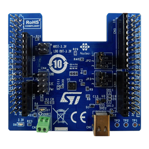
The X-NUCLEO-GFX02Z1 expansion board adds graphic user interface (GUI) capability to STM32 Nucleo-144 boards.
It features a 2.2” 8-bit parallel interface TFT display as well as a 64-Mbit Q-SPI NOR Flash memory for storing graphic images,
texts and texture. The expansion board also offers a joystick for GUI navigation.
X-NUCLEO-GFX02Z1 features the Zio connector. It is compatible with the NUCLEO-F412ZG, NUCLEO-F413ZH, NUCLEO-
F446ZE, NUCLEO-F722ZE, NUCLEO-F746ZG, NUCLEO-F756ZG, NUCLEO-F767ZI, NUCLEO-H743ZI, NUCLEO-H723ZG,
NUCLEO-H753ZI, NUCLEO-H745ZI-Q, NUCLEO-H755ZI-Q, NUCLEO-H7A3ZI-Q, NUCLEO-L496ZG, NUCLEO-L496ZG-P,
NUCLEO-L4A6ZG, NUCLEO-L4P5ZG, NUCLEO-L4R5ZI, NUCLEO-L4R5ZI-P, NUCLEO-L552ZE-Q and NUCLEO-U575ZI-Q
Nucleo-144 boards.
Figure 1. X-NUCLEO-GFX02Z1 top view Figure 2. X-NUCLEO-GFX02Z1 bottom view
Pictures are not contractual.
Display expansion board for STM32 Nucleo-144
UM2905
User manual
UM2905 - Rev 2 - November 2021
For further information contact your local STMicroelectronics sales office. www.st.com

1Features
• 2.2” 8-bit parallel interface QVGA TFT LCD
• 64-Mbit Q-SPI NOR Flash memory
• Joystick for easy menu navigation
• Compatible with selected STM32 Nucleo-144 boards using the Zio connector
UM2905
Features
UM2905 - Rev 2 page 2/24

2Ordering information
To order the X-NUCLEO-GFX02Z1 module, refer to Table 1.
Table 1. Ordering information
Order code Board reference
X-NUCLEO-GFX02Z1 MB1818
The STM32 Nucleo-144 boards feature STM32 32-bit microcontrollers based on the Arm® Cortex®‑M processor.
Note: Arm is a registered trademark of Arm Limited (or its subsidiaries) in the US and/or elsewhere.
UM2905
Ordering information
UM2905 - Rev 2 page 3/24

3Development environment
3.1 Demonstration software
The demonstration software supporting the X-NUCLEO-GFX02Z1 expansion board is available from the X-CUBE-
DISPLAY STM32Cube Expansion Package and must be programmed into the corresponding Nucleo-144 board.
The latest versions of the demonstration source code and associated documentation can be downloaded from
www.st.com.
UM2905
Development environment
UM2905 - Rev 2 page 4/24

4Quick start
Before the first use, make sure that no damage occurred to the board during shipment:
• All socketed components must be firmly secured in their sockets
• Nothing should be loose in the board plastic bag or in the box
To start using the X-NUCLEO-GFX02Z1 expansion board, follow the steps below:
1. Plug the board onto a compatible STM32 Nucleo-144 development board
2. Download the evaluation firmware and full documentation set from www.st.com/en/product/x-cube-display
and program the target device
3. Evaluate the graphic possibilities of STM32 devices combined with the TouchGFX Engine graphic library in
X-CUBE-TOUCHGFX or develop your own application
UM2905
Quick start
UM2905 - Rev 2 page 5/24

5Hardware layout and configuration
Figure 3 and Figure 4 help users to locate the different features on the X-NUCLEO-GFX02Z1 board. The
mechanical dimensions of the X-NUCLEO-GFX02Z1 product are shown in Figure 5.
Figure 3. X-NUCLEO-GFX02Z1 PCB layout: top side
2.2" QVGA TFT
LCD (LCD1)
Menu navigation
joystick (B1)
UP
UM2905
Hardware layout and configuration
UM2905 - Rev 2 page 6/24

Figure 4. X-NUCLEO-GFX02Z1 PCB layout: bottom side
64-Mbit Q-SPI NOR
Flash memory (U1)
LCD ZIF connector
(CN1)
ST Zio connectors
(CN7, CN8, CN9,
CN10)
UM2905
Hardware layout and configuration
UM2905 - Rev 2 page 7/24

Figure 5. X-NUCLEO-GFX02Z1 mechanical drawing
UM2905
Hardware layout and configuration
UM2905 - Rev 2 page 8/24

5.1 Power supply
The X-NUCLEO-GFX02Z1 is directly powered by a 3.3 V power supply provided by the Nucleo-144 development
board through pin 7 of the CN8 connector.
5.2 8-bit parallel interface QVGA TFT LCD (LCD1)
5.2.1 Description
The 8-bit parallel interface QVGA TFT LCD is connected to the 8-bit parallel interface (D0 to D7) of the STM32
device.
5.2.2 Operating voltage
The LCD is designed to operate only with a 3.3 V compatible interface.
5.2.3 I/O interface
Table 2. I/O configuration of the LCD
Pin number Pin name Signal name STM32 GPIO Function
1 LED_K4 - - Display backlight LED4 cathode
2 IM0 GND -
System interface selection: 80 MCU 8-bit bus interface I
3 IM1 GND -
4 IM2 GND -
5 IM3 GND -
6 RESET DISP_NRESET PE11 Reset active low
7 - 20 - - - Not connected
21 DB7 DISP_D7 PE10
Data bus
22 DB6 DISP_D6 PE9
23 DB5 DISP_D5 PE8
24 DB4 DISP_D4 PE7
25 DB3 DISP_D3 PD1
26 DB2 DISP_D2 PD0
27 DB1 DISP_D1 PD15
28 DB0 DISP_D0 PD14
29 - - - Not connected
30 - - - Not connected
31 RD DISP_NOE PD4 Read enable
32 RS DISP_DCX PE4 Data or Command select
33 WR DISP_NWE PD5 Write enable
34 CS DISP_NE1 PD7 Chip select
35 FMARK DISP_TE PE13 Tearing effect output pin to synchronize MCU on frame writing
36 VCC 3V3 - 3.3 V power supply
37 GND GND - Ground
38 LED_A 3V3 - Display backlight LED common anode
39 LED_K1 - - Display backlight LED1 cathode
UM2905
Power supply
UM2905 - Rev 2 page 9/24

Pin number Pin name Signal name STM32 GPIO Function
40 LED_K2 - - Display backlight LED2 cathode
41 LED_K3 - - Display backlight LED3 cathode
42 - - - Not connected
43 INT INT PE5 Reserved for touch panel
44 I2C_SCL I2C_SCL PF1(1)
PF14(2) Reserved for touch panel
45 I2C_SDA I2C_SDA PF0(1)
PF15(2) Reserved for touch panel
1. NUCLEO-F412ZG, NUCLEO-F413ZH, NUCLEO-F446ZE, NUCLEO-F722ZE, NUCLEO-F746ZG, NUCLEO-F756ZG,
NUCLEO-F767ZI, NUCLEO-H743ZI, NUCLEO-H723ZG, NUCLEO-H753ZI, NUCLEO-L496ZG, NUCLEO-L496ZG-P,
NUCLEO-L4A6ZG, NUCLEO-L4P5ZG, NUCLEO-L4R5ZI, NUCLEO-L4R5ZI-P, NUCLEO-L552ZE-Q, NUCLEO-U575ZI-Q.
2. NUCLEO-H745ZI-Q, NUCLEO-H755ZI-Q, NUCLEO-H7A3ZI-Q.
5.3 Q-SPI NOR Flash memory (U1)
5.3.1 Description
The 64-Mbit Q-SPI NOR Flash memory is connected to a Q-SPI interface of the STM32 device and can be used
to store graphic objects. The use of Q-SPI ensures optimum data transfer between the Flash memory and the
LCD display.
5.3.2 Operating voltage
The NOR Flash memory is designed to operate only with a 3.3 V Q-SPI interface.
UM2905
Q-SPI NOR Flash memory (U1)
UM2905 - Rev 2 page 10/24

5.3.3 I/O interface
Table 3. I/O configuration of the NOR Flash memory
Pin number Pin name Signal name STM32 GPIO Function
1 CS# QSPI_NCS
PB6(1)
PG6(2)
PA2(3)
Chip select active high
2 SIO1 QSPI_IO1 PD12(1) (2)
PB0(3) Q-SPI I/O1
3 SIO2 QSPI_IO2 PE2(1) (2)
PE14(3) Q-SPI I/O2
4 GND GND - Ground
5 SIO0 QSPI_IO0 PD11(1) (2)
PE12(3) Q-SPI I/O0
6 SCLK QSPI_CLK PB2(1) (2)
PB10(3) Q-SPI clock
7 SIO3 QSPI_IO3 PD13(1) (2)
PE15(3) Q-SPI I/O3
8 VCC 3V3 - 3.3 V power supply
1. NUCLEO-F412ZG, NUCLEO-F413ZH, NUCLEO-F446ZE, NUCLEO-F722ZE, NUCLEO-F746ZG, NUCLEO-F756ZG,
NUCLEO-F767ZI.
2. NUCLEO-H743ZI, NUCLEO-H723ZG, NUCLEO-H753ZI, NUCLEO-H745ZI-Q, NUCLEO-H755ZI-Q, NUCLEO-H7A3ZI-Q.
3. NUCLEO-L496ZG, NUCLEO-L496ZG-P, NUCLEO-L4A6ZG, NUCLEO-L4P5ZG, NUCLEO-L4R5ZI, NUCLEO-L4R5ZI-P,
NUCLEO-L552ZE-Q, NUCLEO-U575ZI-Q.
5.4 Joystick (B1)
5.4.1 Description
The joystick (B1) allows the navigation within the menu displayed on the LCD.
5.4.2 I/O interface
Table 4. I/O configuration of the joystick
Pin number Pin name Signal name STM32 GPIO Function
1 LEFT KEY_LEFT PE3 Joystick left direction (active low)
2 CENTER KEY_CENTER PA0 Joystick center (active low)
3 DOWN KEY_DOWN PF8 Joystick down direction (active low)
4 UP KEY_UP PF9 Joystick up direction (active low)
5 COMMON GND - Common connected to ground
6 RIGHT KEY_RIGHT PF7 Joystick right direction (active low)
UM2905
Joystick (B1)
UM2905 - Rev 2 page 11/24

5.5 Zio connectors (CN7, CN8, CN9 and CN10)
5.5.1 Description
The Zio connectors allow the X-NUCLEO-GFX02Z1 connection to a standard Nucleo-144 development board.
5.5.2 I/O interface
Figure 6. Zio connectors pinout
1
21
CN8
CN7
2
15 16
2019
CN9 CN10
1 2
29 30 3433
21
UM2905
Zio connectors (CN7, CN8, CN9 and CN10)
UM2905 - Rev 2 page 12/24

Table 5. I/O configuration of Zio connector CN7
Pin number Pin name Signal name STM32 GPIO Function
1 - 7 - - - Not connected
8 GND - - Ground
9 - 15 - - - Not connected
16 DB0 DISP_D0 PD14 Data bus
17 - - - Not connected
18 DB1 DISP_D1 PD15 Data bus
19 – 20 - - - Not connected
Table 6. I/O configuration of Zio connector CN8
Pin number Pin name Signal name STM32 GPIO Function
1 - 6 - - - Not connected
7 VCC 3V3 - 3.3 V power supply
8 - 10 - - - Not connected
11 GND - - Ground
12 - - - Not connected
13 GND - - Ground
14-16 - - - Not connected
UM2905
Zio connectors (CN7, CN8, CN9 and CN10)
UM2905 - Rev 2 page 13/24

Table 7. I/O configuration of Zio connector CN9
Pin number Pin name Signal name STM32 GPIO Function
1 - - - Not connected
2 CS DISP_NE1 PD7 Chip select
3 - 5 - - - Not connected
6 WR DISP_NWE PD5 Write enable
7 - - - Not connected
8 RD DISP_NOE PD4 Read enable
9 - 11 - - - Not connected
12 GND - - Ground
13 -14 - - - Not connected
15 DB6 DISP_D6 PE9 Data bus
16 RS DISP_DCX PE4 Data or command select
17 - - - Not connected
18 INT INT PE5 Reserved for touch panel
19 I2C_SCL I2C_SCL PF1(1)
PF14(2) Reserved for touch panel
20 - - - Not connected
21 I2C_SDA I2C_SDA PF0(1)
PF15(2) Reserved for touch panel
22 LEFT KEY_LEFT PE3 Joystick left direction (active low)
23 GND - - Ground
24 DOWN KEY_DOWN PF8 Joystick down direction (active low)
25 DB2 DISP_D2 PD0 Data bus
26 RIGHT KEY_RIGHT PF7 Joystick right direction (active low)
27 DB3 DISP_D3 PD1 Data bus
28 UP KEY_UP PF9 Joystick up direction (active low)
29 - 30 - - - Not connected
1. NUCLEO-F412ZG, NUCLEO-F413ZH, NUCLEO-F446ZE, NUCLEO-F722ZE, NUCLEO-F746ZG, NUCLEO-F756ZG,
NUCLEO-F767ZI, NUCLEO-H743ZI, NUCLEO-H723ZG, NUCLEO-H753ZI, NUCLEO-L496ZG, NUCLEO-L496ZG-P,
NUCLEO-L4A6ZG, NUCLEO-L4P5ZG, NUCLEO-L4R5ZI, NUCLEO-L4R5ZI-P, NUCLEO-L552ZE-Q, NUCLEO-U575ZI-Q.
2. NUCLEO-H745ZI-Q, NUCLEO-H755ZI-Q, NUCLEO-H7A3ZI-Q.
UM2905
Zio connectors (CN7, CN8, CN9 and CN10)
UM2905 - Rev 2 page 14/24

Table 8. I/O configuration of Zio connector CN10
Pin number Pin name Signal name STM32 GPIO Function
1-3 - - - Not connected
4 DB6 DISP_D6 PE9 Data bus
5 GND - - Ground
6 RESET DISP_NRESET PE11 Reset active low
7-9 - - - Not connected
10 FMARK DISP_TE PE13 Tearing effect output pin to synchronize MCU on frame writing
11 - 12 - - - Not connected
13 CS# QSPI_NCS
PB6(1)
PG6(2)
PA2(3)
Chip select active high
14 - - - Not connected
15 SCLK QSPI_CLK PB2(1) (2)
PB10(3) Q-SPI clock
16 - - - Not connected
17 GND - - Ground
18 DB5 DISP_D5 PE8 Data bus
19 SIO3 QSPI_IO3 PD13(1) (2)
PE15(3) Q-SPI I/O3
20 DB4 DISP_D4 PE7 Data bus
21 SIO1 QSPI_IO1 PD12(1) (2)
PB0(3) Q-SPI I/O1
22 GND - - Ground
23 SIO0 QSPI_IO0 PD11(1) (2)
PE12(3) Q-SPI I/O0
24 DB7 DISP_D7 PE10 Data bus
25 SIO2 QSPI_IO2 PE2(1) (2)
PE14(3) Q-SPI I/O2
26 - - - Not connected
27 GND - - Ground
28 - - - Not connected
29 CENTER KEY_CENTER PA0 Joystick center (active low)
30 - 34 - - - Not connected
1. NUCLEO-F412ZG, NUCLEO-F413ZH, NUCLEO-F446ZE, NUCLEO-F722ZE, NUCLEO-F746ZG, NUCLEO-F756ZG,
NUCLEO-F767ZI.
2. NUCLEO-H743ZI, NUCLEO-H723ZG, NUCLEO-H753ZI, NUCLEO-H745ZI-Q, NUCLEO-H755ZI-Q, NUCLEO-H7A3ZI-Q.
3. NUCLEO-L496ZG, NUCLEO-L496ZG-P, NUCLEO-L4A6ZG, NUCLEO-L4P5ZG, NUCLEO-L4R5ZI, NUCLEO-L4R5ZI-P,
NUCLEO-L552ZE-Q, NUCLEO-U575ZI-Q.
UM2905
Zio connectors (CN7, CN8, CN9 and CN10)
UM2905 - Rev 2 page 15/24

6Product information
6.1 Product marking
The stickers located on the top or bottom side of the PCB provide product information:
• Product order code and product identification for the first sticker
• Board reference with revision, and serial number for the second sticker
On the first sticker, the first line provides the product order code, and the second line the product identification.
On the second sticker, the first line has the following format: “MBxxxx-Variant-yzz”, where “MBxxxx” is the board
reference, “Variant” (optional) identifies the mounting variant when several exist, "y" is the PCB revision and "zz"
is the assembly revision, for example B01. The second line shows the board serial number used for traceability.
Evaluation tools marked as “ES” or “E” are not yet qualified and therefore not ready to be used as reference
design or in production. Any consequences deriving from such usage will not be at ST charge. In no event, ST will
be liable for any customer usage of these engineering sample tools as reference designs or in production.
“E” or “ES” marking location is next to the evaluation tool ordering part number that is stuck or silk-screen printed
on the board.
6.2 X-NUCLEO-GFX02Z1 product history
6.2.1 Product identification XNGFX02Z1$AZ1
This product identification is based on board MB1818-DT022CTFT-B01. The LCD used in this product is
DT022CTFT with driver IC ILI9341V.
Product limitations
No limitation identified for this product identification.
6.2.2 Product identification XNGFX02Z1$AZ2
This product identification is based on board MB1818-TCXD022IB5-B01. The LCD used in this product is
TCXD022IBLON-5 with driver IC ST7789V.
Product limitations
No limitation identified for this product identification.
6.3 Board revision history
6.3.1 Board MB1818 revision B-01
The revision B-01 is the initial release of board MB1818.
Board limitations
No limitation identified for this board revision.
UM2905
Product information
UM2905 - Rev 2 page 16/24

7Federal Communications Commission (FCC) and ISED Canada
Compliance Statements
7.1 FCC Compliance Statement
Part 15.19
This device complies with Part 15 of the FCC Rules. Operation is subject to the following two conditions: (1) this
device may not cause harmful interference, and (2) this device must accept any interference received, including
interference that may cause undesired operation.
Part 15.21
Any changes or modifications to this equipment not expressly approved by STMicroelectronics may cause
harmful interference and void the user's authority to operate this equipment.
Part 15.105
This equipment has been tested and found to comply with the limits for a Class B digital device, pursuant to part
15 of the FCC Rules. These limits are designed to provide reasonable protection against harmful interference
in a residential installation. This equipment generates uses and can radiate radio frequency energy and, if not
installed and used in accordance with the instruction, may cause harmful interference to radio communications.
However, there is no guarantee that interference will not occur in a particular installation. If this equipment does
cause harmful interference to radio or television reception which can be determined by turning the equipment off
and on, the user is encouraged to try to correct interference by one or more of the following measures:
• Reorient or relocate the receiving antenna.
• Increase the separation between the equipment and receiver.
• Connect the equipment into an outlet on circuit different from that to which the receiver is connected.
• Consult the dealer or an experienced radio/TV technician for help.
Note: Use only shielded cables.
Responsible party (in the USA)
Terry Blanchard
Americas Region Legal | Group Vice President and Regional Legal Counsel, The Americas
STMicroelectronics, Inc.
750 Canyon Drive | Suite 300 | Coppell, Texas 75019
USA
Telephone: +1 972-466-7845
7.2 ISED Compliance Statement
ISED Canada ICES-003 Compliance Label: CAN ICES-3 (B) / NMB-3 (B).
Étiquette de conformité à la NMB-003 d'ISDE Canada: CAN ICES-3 (B) / NMB-3 (B).
UM2905
Federal Communications Commission (FCC) and ISED Canada Compliance Statements
UM2905 - Rev 2 page 17/24

8CE conformity
8.1 Warning
EN 55032 / CISPR32 (2012) Class B product
Warning: this device is compliant with Class B of EN55032 / CISPR32. In a residential environment, this
equipment may cause radio interference.
Avertissement : cet équipement est conforme à la Classe B de la EN55032 / CISPR 32. Dans un environnement
résidentiel, cet équipement peut créer des interférences radio.
UM2905
CE conformity
UM2905 - Rev 2 page 18/24

Contents
1Features...........................................................................2
2Ordering information ..............................................................3
3Development environment .........................................................4
3.1 Demonstration software .........................................................4
4Quick start ........................................................................5
5Hardware layout and configuration.................................................6
5.1 Power supply ..................................................................9
5.2 8-bit parallel interface QVGA TFT LCD (LCD1) .....................................9
5.2.1 Description .............................................................9
5.2.2 Operating voltage ........................................................9
5.2.3 I/O interface ............................................................9
5.3 Q-SPI NOR Flash memory (U1) .................................................10
5.3.1 Description ............................................................10
5.3.2 Operating voltage .......................................................10
5.3.3 I/O interface ...........................................................11
5.4 Joystick (B1) .................................................................11
5.4.1 Description ............................................................11
5.4.2 I/O interface ...........................................................11
5.5 Zio connectors (CN7, CN8, CN9 and CN10) .......................................12
5.5.1 Description ............................................................12
5.5.2 I/O interface ...........................................................12
6Product information ..............................................................16
6.1 Product marking ..............................................................16
6.2 X-NUCLEO-GFX02Z1 product history ............................................16
6.2.1 Product identification XNGFX02Z1$AZ1 ......................................16
6.2.2 Product identification XNGFX02Z1$AZ2 ......................................16
6.3 Board revision history ..........................................................16
6.3.1 Board MB1818 revision B-01 ..............................................16
7Federal Communications Commission (FCC) and ISED Canada Compliance
Statements .......................................................................17
UM2905
Contents
UM2905 - Rev 2 page 20/24
Table of contents
Other ST Computer Hardware manuals

ST
ST I-CUBE-LRWAN User manual

ST
ST X-NUCLEO-IDW01M1 User manual

ST
ST STEVAL-IFP043V1 User manual

ST
ST ST25DV-DISCOVERY User manual

ST
ST X-NUCLEO-OUT10A1 User manual

ST
ST UM2727 User manual
ST
ST 32F412GDISCOVERY User manual

ST
ST STSW-L9026-Y0 User manual

ST
ST X-NUCLEO-OUT17A1 User manual

ST
ST MotionTL User manual

ST
ST UM2960 User manual

ST
ST STEVAL-IDB013V1 Administrator Guide

ST
ST AEK-COM-ISOSPI1 User manual

ST
ST STDES-PFCBIDIR User manual

ST
ST X-LINUX-NFC5 User manual

ST
ST X-NUCLEO-SNK1M1 User manual

ST
ST X-NUCLEO-OUT01A2 User manual

ST
ST STM32 Nucleo User manual

ST
ST STM32F4 Series Owner's manual

ST
ST STDES-65ACFADP Specification sheet