Texas Instruments TPS54335AEVM-010 User manual
Other Texas Instruments Control Unit manuals
Texas Instruments
Texas Instruments DP83869EVM User manual
Texas Instruments
Texas Instruments TA 5 1 Q15B5EVM-K Series User manual
Texas Instruments
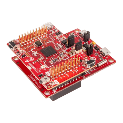
Texas Instruments TPS6021 Series User manual
Texas Instruments
Texas Instruments SimpleLink Wi-Fi CC3 20 Series User manual

Texas Instruments
Texas Instruments TPS54383 User manual
Texas Instruments
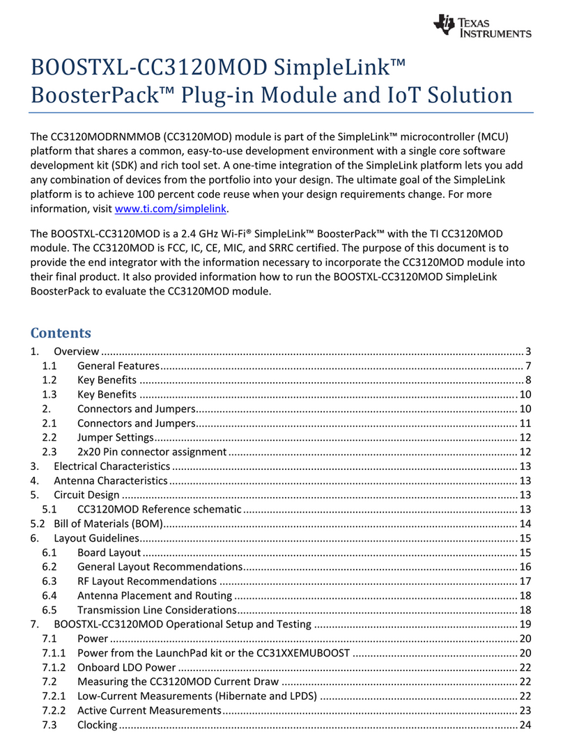
Texas Instruments SimpleLink BoosterPack BOOSTXL-CC3120MOD User manual
Texas Instruments
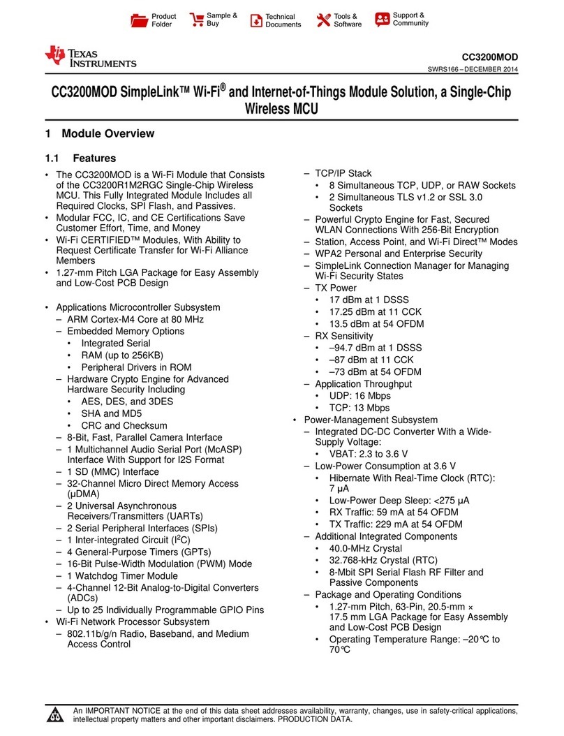
Texas Instruments SimpleLink CC3200MOD User manual

Texas Instruments
Texas Instruments BOOSTXL-TPS652170 User manual
Texas Instruments
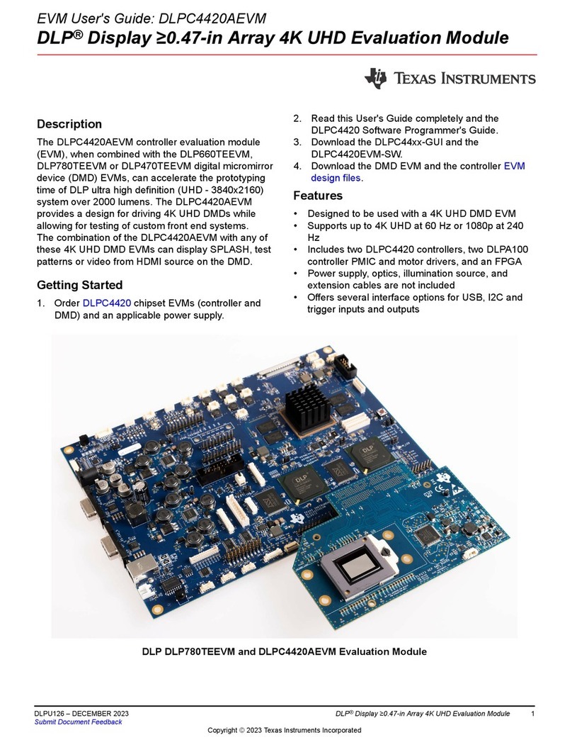
Texas Instruments DLP DLPC4420AEVM User manual
Texas Instruments
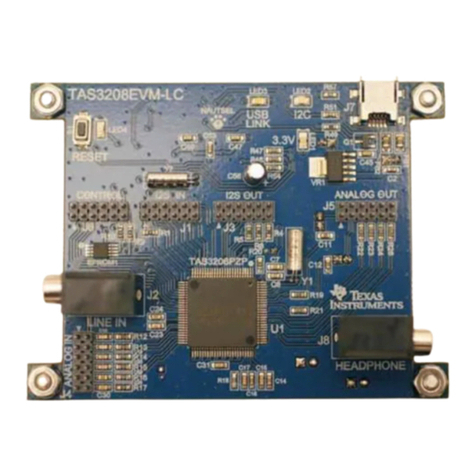
Texas Instruments TAS3208EVM-LC User manual
Texas Instruments
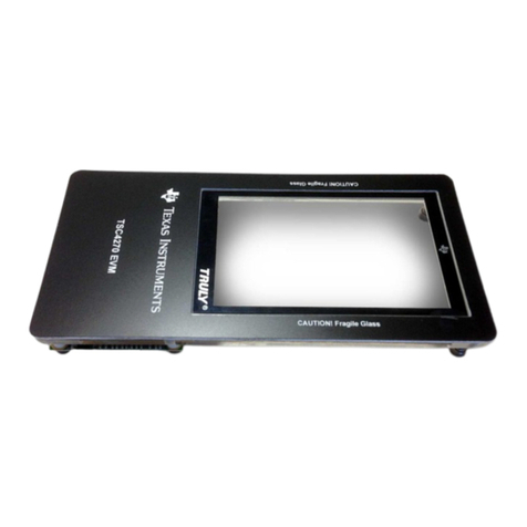
Texas Instruments TSC4270 User manual
Texas Instruments
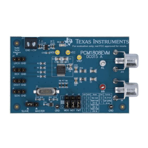
Texas Instruments PCM1808EVM User manual
Texas Instruments
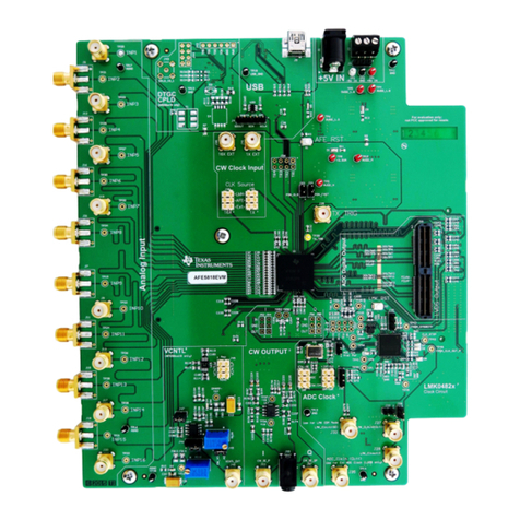
Texas Instruments AFE5818 User manual
Texas Instruments
Texas Instruments PurePath Digital TAS5342DDV6EVM User manual
Texas Instruments
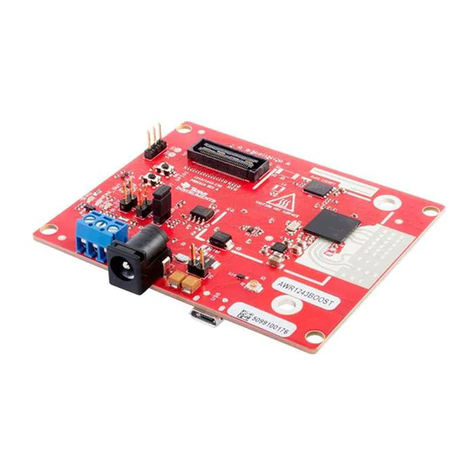
Texas Instruments AWR1443 User manual
Texas Instruments
Texas Instruments CC256xEM User manual
Texas Instruments
Texas Instruments 2000 series User manual
Texas Instruments
Texas Instruments TPA4411 User manual
Texas Instruments
Texas Instruments TMCS1101EVM User manual
Texas Instruments
Texas Instruments TPS92410EVM-001 User manual
Popular Control Unit manuals by other brands
Festo
Festo Compact Performance CP-FB6-E Brief description
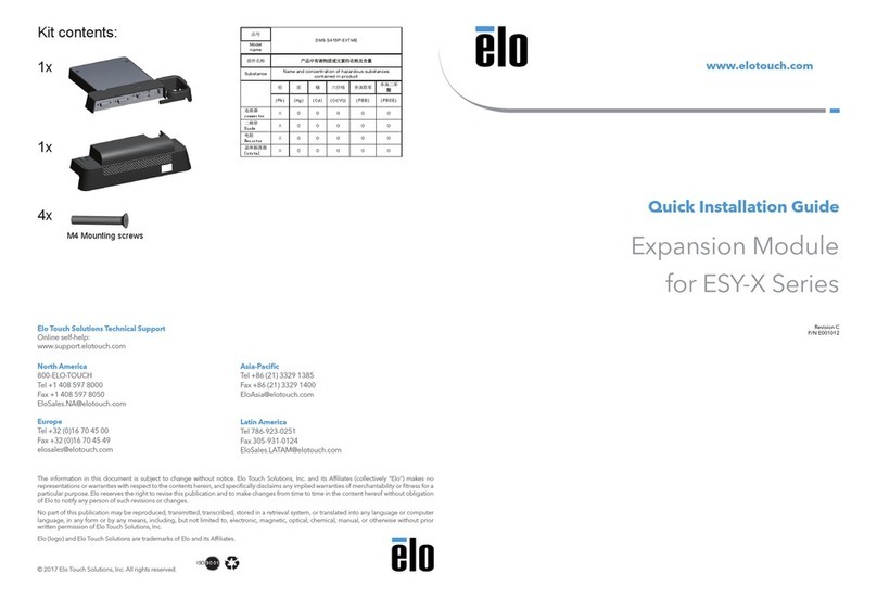
Elo TouchSystems
Elo TouchSystems DMS-SA19P-EXTME Quick installation guide
JS Automation
JS Automation MPC3034A user manual
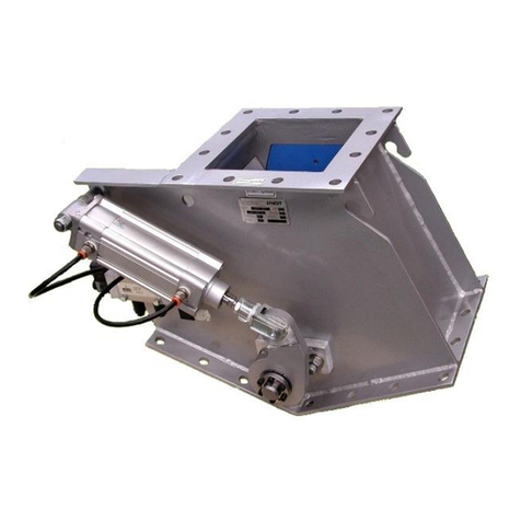
JAUDT
JAUDT SW GII 6406 Series Translation of the original operating instructions
Spektrum
Spektrum Air Module System manual
BOC Edwards
BOC Edwards Q Series instruction manual

KHADAS
KHADAS BT Magic quick start
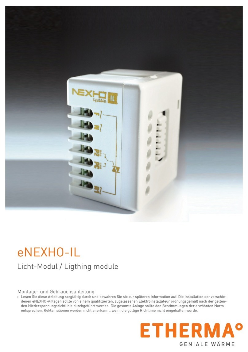
Etherma
Etherma eNEXHO-IL Assembly and operating instructions
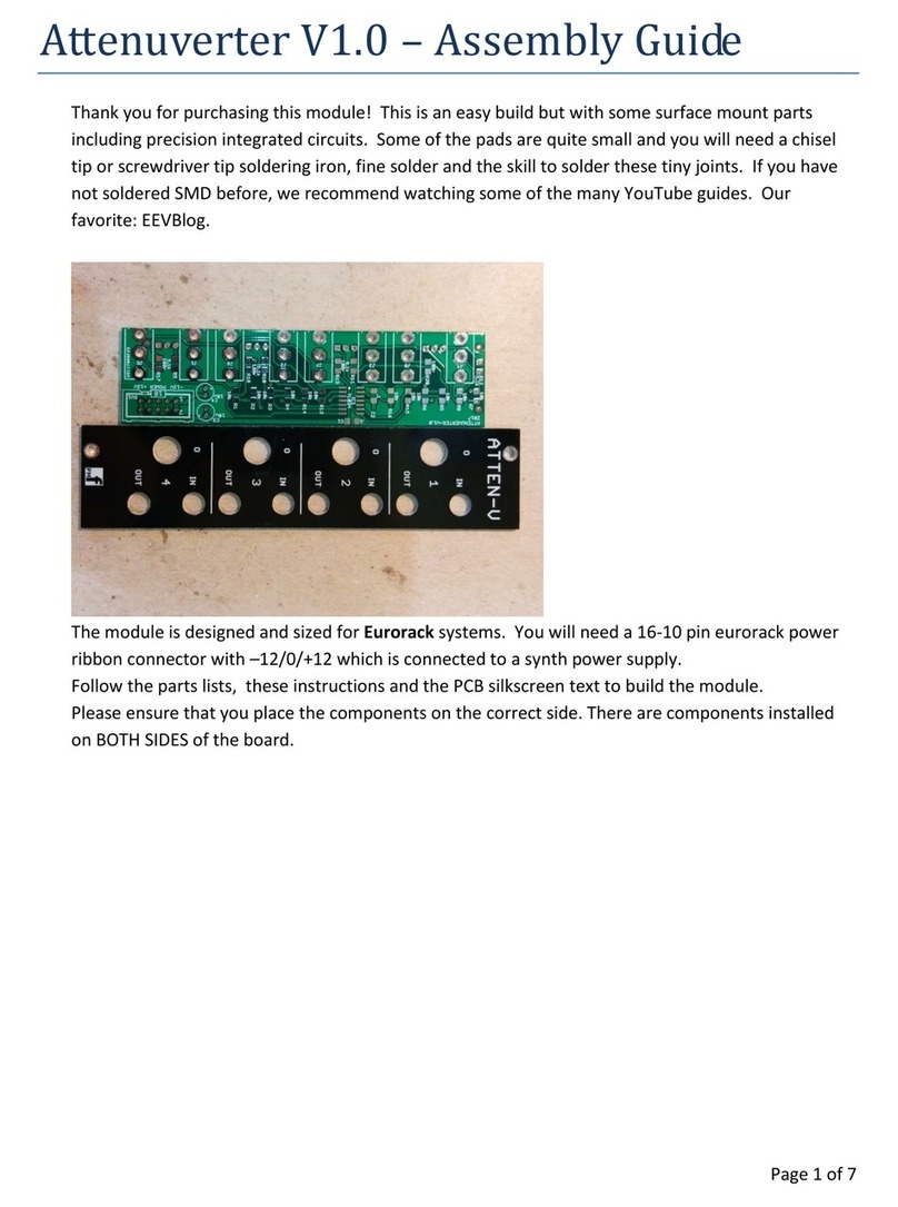
PMFoundations
PMFoundations Attenuverter Assembly guide
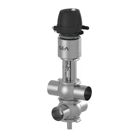
GEA
GEA VARIVENT Operating instruction
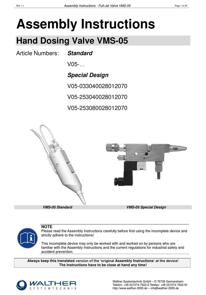
Walther Systemtechnik
Walther Systemtechnik VMS-05 Assembly instructions
Altronix
Altronix LINQ8PD Installation and programming manual
